Hi,
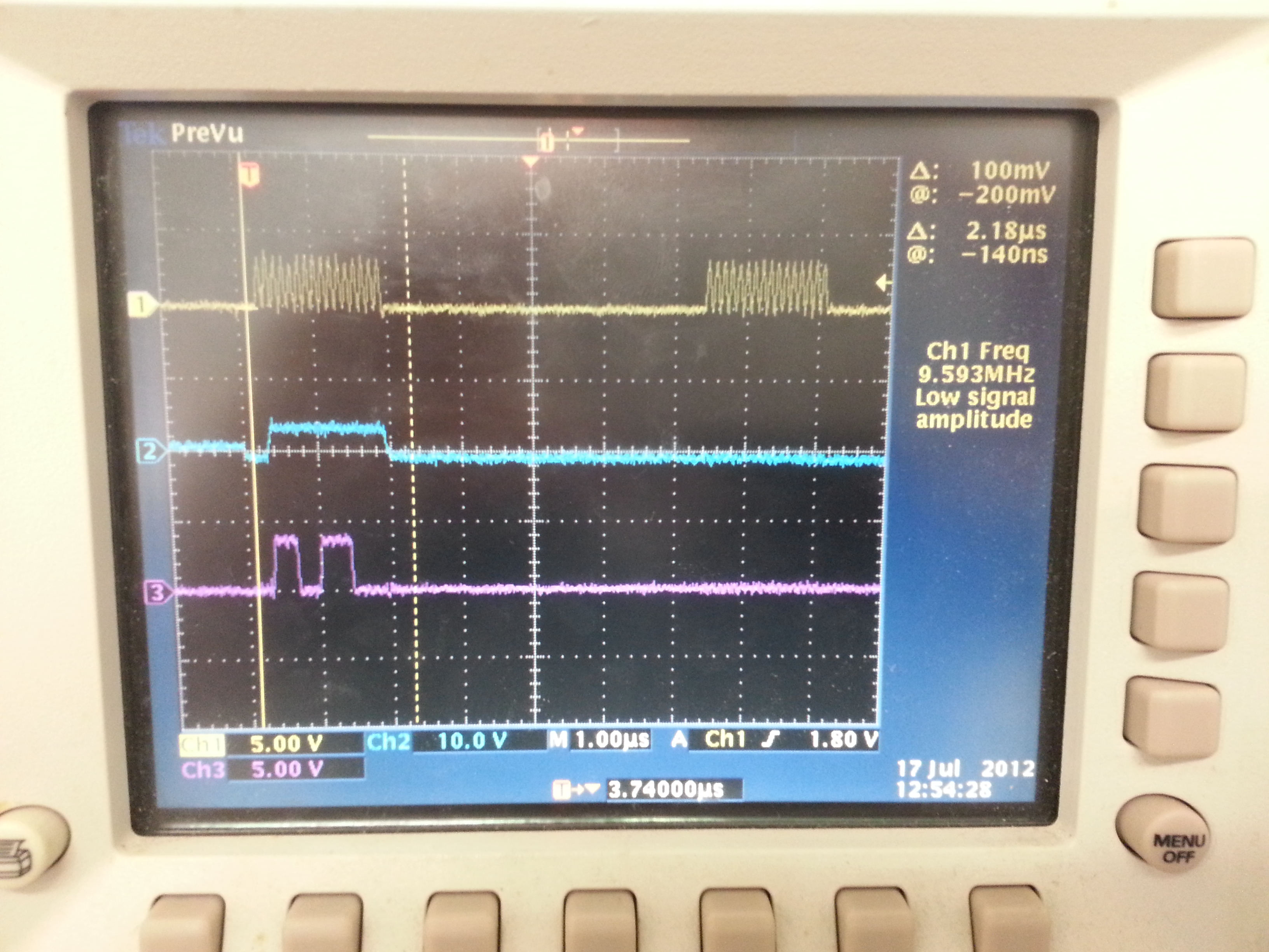
I'm currently having problems communicating via 4-wire SPI between the F28335 and the AD7699. I believe I have the SPI configured correctly on the F28335 by observing the inputs/outputs on a scope. My main two problems are: 1) while trying to configure the SPI clock above a lower freq (above ~5 MHz) it becomes an ugly triangle wave which could or could not be a problem and 2) It looks like I am sending the proper configuration to the ADC on the MOSI but while on the read back configuration setting, the MISO is not properly reading back the configuration or the correct voltage reading output (3.3 VDC). I have attached a scope print out and code below. I used an example program for the SPI setup. Any help is appreciated, thanks in advance.
#include "DSP28x_Project.h" // Device Headerfile and Examples Include File
void spi_init(void);
Uint16 data1;
Uint16 data2;
void main(void)
{
// Step 1. Initialize System Control:
// PLL, WatchDog, enable Peripheral Clocks
// This example function is found in the DSP2833x_SysCtrl.c file.
InitSysCtrl();
// Step 2. Initalize GPIO:
// This example function is found in the DSP2833x_Gpio.c file and
// illustrates how to set the GPIO to it's default state.
// InitGpio(); // Skipped for this example
// Setup only the GP I/O only for SPI-A functionality
InitSpiaGpio();
// Step 3. Initialize PIE vector table:
// Disable and clear all CPU interrupts
DINT;
IER = 0x0000;
IFR = 0x0000;
// Initialize PIE control registers to their default state:
// This function is found in the DSP2833x_PieCtrl.c file.
InitPieCtrl();
// Initialize the PIE vector table with pointers to the shell Interrupt
// Service Routines (ISR).
// This will populate the entire table, even if the interrupt
// is not used in this example. This is useful for debug purposes.
// The shell ISR routines are found in DSP2833x_DefaultIsr.c.
// This function is found in DSP2833x_PieVect.c.
InitPieVectTable();
// Step 4. Initialize all the Device Peripherals:
// This function is found in DSP2833x_InitPeripherals.c
// InitPeripherals(); // Not required for this example
spi_init(); // Initialize the SPI only
// Step 5. User specific code, enablenfiguration();
while(1)
{
GpioDataRegs.GPBCLEAR.bit.GPIO57 = 1; /* set CS low */
data1 = spiBSendByte(0x71E0); /* keep configuration and read back data from IN0 (71E4) from IN1 (73E4) */
DELAY_US(1);
data1 = spiBSendByte(0); /* read back configuration */
GpioDataRegs.GPBSET.bit.GPIO57 = 1; /* set CS high */
DELAY_US(6);
}
}
int spiBSendByte(const unsigned int data)
{
SpiaRegs.SPITXBUF = data; /* Load TX buffer with data */
DELAY_US(6); /* Delay to load TX buffer */
data2 = SpiaRegs.SPIRXBUF; /* Read data from RX buffer */
return (1);
}
void spi_init() */ SPI setup */
{
Uint16 dummy;
SpiaRegs.SPICCR.bit.SPISWRESET=0; // Reset SPI
SpiaRegs.SPICCR.all=0x000F; //16-bit character
SpiaRegs.SPICTL.bit.MASTER_SLAVE = 1; // Master mode enabled
SpiaRegs.SPICTL.bit.TALK = 1; // Transmit capability enabled
SpiaRegs.SPISTS.all=0x0000;
SpiaRegs.SPIBRR = 0x0002; // Baud rate ~ 10 MHz
SpiaRegs.SPICCR.bit.CLKPOLARITY = 0; // Rise edge w/o delay
SpiaRegs.SPICTL.bit.CLK_PHASE = 0;
SpiaRegs.SPICCR.bit.SPISWRESET=1; // Enable SPI
GpioDataRegs.GPBCLEAR.bit.GPIO57 = 1; /* set CS low */
dummy = spiBSendByte(0xF1E0); /* Set ADC to factory settings by holding DIN high for two conversions */
GpioDataRegs.GPBSET.bit.GPIO57 = 1; /* set CS high */
DELAY_US(10); /* Delay between dummys */
GpioDataRegs.GPBCLEAR.bit.GPIO57 = 1; /* set CS low */
dummy = spiBSendByte(0xF1E0); /* second dummy (F1E4 for IN0) */
GpioDataRegs.GPBSET.bit.GPIO57 = 1; /* set CS high */
}
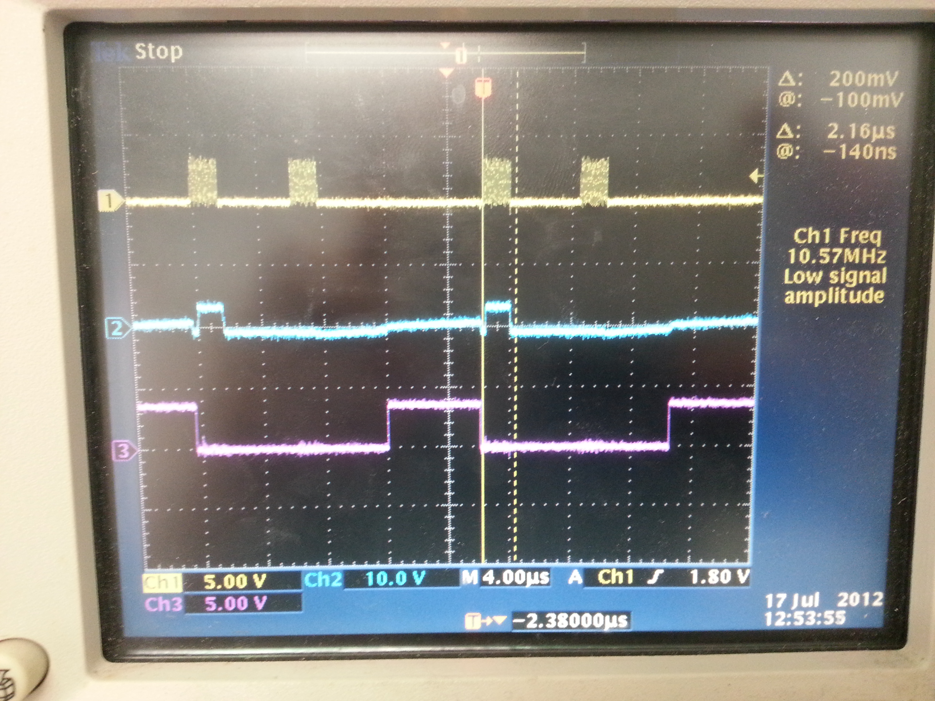
Yellow = clock, blue = MISO, purple = CS (above) or MOSI (below)