This thread has been locked.

If you have a related question, please click the "Ask a related question" button in the top right corner. The newly created question will be automatically linked to this question.

Problem waking device from LPM Halt state with a particular GPIO pin (GPIO29)

Other Parts Discussed in Thread: TMS320F28334

I'm using a TMS320F28334 in a design and it is behaving unexpectedly when trying to use GPIO29 as a source to wake processor from LPM halt state.  I am using a few other GPIO pins to wake the device without any issues.  

After setting GpioIntRegs.GPIOLPMSEL.all = 0x20000000,(GPIO29 selected as wake source), and putting the device into Halt LPM state, the device does the following:

When there is a falling edge on GPIO29, the unit processor does not wake.  If other GPIO are selected as wake sources along with GPIO29 they no longer wake the processor after GPIO29 goes low.  The device is stuck.  Only when GPIO29 transitions high does the processor wake up.  This is counter to what the datasheet describes.  The datasheet states that only negative transitions can wake the processor.  This seems to be the case for all other GPIO I am using as wake sources.

I have experimented with aggressively filtering the signal on GPIO29 with an RC filter.  I even put a filter cap directly beneath the GPIO29 BGA pin.  The behavior is the same.  I do not observe any noise or glitching on this line on the oscilloscope so I don't think this is noise related.

The problem is consistent on multiple boards with different processors.

Any ideas?

Thanks!

  • Hi Jason,

    I'm looking into your problem right now.

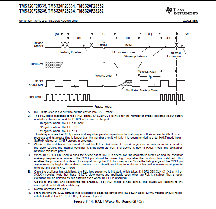
    My understanding is: your device is in HALT mode; and in order to wake it you've determind you need a pulse as opposed to a falling edge.

    Looking at the timing diagram for Halt Wake-up it appears the pin could need to be pulled high after the PLL has stabilized. But that there is a necessary wait time of toscst + 2tc(OSCCLK) (Figure 6-18 HALT Mode Timing Requirements)

    I'm investigating further as to whether this is a coincidence in the timing diagram or a necessity. But based on the requirements for exiting IDLE mode I suspect a pulse may be necessary.

    -Louis

  • Hi Jason,

    I looked into your problem with our factory guys, the F 2833x devices need to be pulsed to be woken from HALT mode.

    The spec listed in the data sheet is the minimum time it takes for the PLL to stabilize. In other words, it's the smallest pulse you can send to safely wake the processor.

    On the first low transistion the device wakes and starts the clocks but code execution wont commence until a high transition.

    I attached an example that places a 2833x in HALT and toggles an output after exiting.

    Hope this solves your problem!

    Thanks,

     Louis

    // TI File $Revision: /main/13 $
    // Checkin $Date: June 19, 2008   17:08:02 $
    //###########################################################################
    //
    // FILE:    Example_2833xHaltWake.c
    //
    // TITLE:   Device Halt Mode and Wakeup Program.
    //
    // ASSUMPTIONS:
    //
    //    This program requires the DSP2833x header files.
    //
    //    GPIO0 is configured as the LPM wakeup pin to trigger a
    //    WAKEINT interrupt upon detection of a low pulse.
    //    Initially, pull GPIO0 high externally. To wake device
    //    from halt mode, pull GPIO0 low for at least the crystal
    //    startup time + 2 OSCLKS, then pull it high again.
    //
    //    To observe when device wakes from HALT mode, monitor
    //    GPIO1 with an oscilloscope (set to 1 in WAKEINT ISR)
    //
    //    As supplied, this project is configured for "boot to SARAM"
    //    operation.  The 2833x Boot Mode table is shown below.
    //    For information on configuring the boot mode of an eZdsp,
    //    please refer to the documentation included with the eZdsp,
    //
    //       $Boot_Table:
    //
    //         GPIO87   GPIO86     GPIO85   GPIO84
    //          XA15     XA14       XA13     XA12
    //           PU       PU         PU       PU
    //        ==========================================
    //            1        1          1        1    Jump to Flash
    //            1        1          1        0    SCI-A boot
    //            1        1          0        1    SPI-A boot
    //            1        1          0        0    I2C-A boot
    //            1        0          1        1    eCAN-A boot
    //            1        0          1        0    McBSP-A boot
    //            1        0          0        1    Jump to XINTF x16
    //            1        0          0        0    Jump to XINTF x32
    //            0        1          1        1    Jump to OTP
    //            0        1          1        0    Parallel GPIO I/O boot
    //            0        1          0        1    Parallel XINTF boot
    //            0        1          0        0    Jump to SARAM	    <- "boot to SARAM"
    //            0        0          1        1    Branch to check boot mode
    //            0        0          1        0    Boot to flash, bypass ADC cal
    //            0        0          0        1    Boot to SARAM, bypass ADC cal
    //            0        0          0        0    Boot to SCI-A, bypass ADC cal
    //                                              Boot_Table_End$
    //
    // DESCRIPTION:
    //
    //    This example puts the device into HALT mode. If the lowest
    //    possible current consumption in HALT mode is desired, the
    //    JTAG connector must be removed from the device board while
    //    the device is in HALT mode.
    //
    //    The example then wakes up the device from HALT using GPIO0.
    //    GPIO0 wakes the device from HALT mode when a low pulse
    //    (signal goes high->low->high)is detected on the pin.
    //    This pin must be pulsed by an external agent for wakeup.
    //
    //    As soon as GPIO0 goes high again after the pulse, the device
    //    should wake up, and GPIO1 can be observed to toggle.
    //
    //
    //###########################################################################
    // $TI Release: DSP2833x/DSP2823x Header Files V1.20 $
    // $Release Date: August 1, 2008 $
    //###########################################################################
    
    #include "DSP28x_Project.h"     // Device Headerfile and Examples Include File
    
    // Prototype statements for functions found within this file.
    
    interrupt void WAKE_ISR(void);  	// ISR for WAKEINT
    
    void main()
    
    {
    
       asm("  EALLOW");
    
    // Step 1. Initialize System Control:
    // PLL, WatchDog, enable Peripheral Clocks
    // This example function is found in the DSP2833x_SysCtrl.c file.
       InitSysCtrl();
    
    // Step 2. Initalize GPIO:
    // This example function is found in the DSP2833x_Gpio.c file and
    // illustrates how to set the GPIO to it's default state.
    // InitGpio();  // Skipped for this example
    //  Enable all pull-ups
        EALLOW;
    	GpioCtrlRegs.GPAPUD.all = 0;
    	GpioCtrlRegs.GPBPUD.all = 0;
    	GpioCtrlRegs.GPADIR.bit.GPIO1 = 1;	    // GPIO1 set in the ISR to indicate device woken up.
        GpioCtrlRegs.GPBDIR.bit.GPIO32 = 1;
        //GpioIntRegs.GPIOLPMSEL.bit.GPIO0 = 1;	// Choose GPIO0 pin for wakeup
    	// I am using GPIO14
    	GpioIntRegs.GPIOLPMSEL.bit.GPIO14 = 1;
    	EDIS;
    
    /// Step 3. Clear all interrupts and initialize PIE vector table:
    // Disable CPU interrupts
       DINT;
    
    // Initialize the PIE control registers to their default state.
    // The default state is all PIE interrupts disabled and flags
    // are cleared.
    // This function is found in the DSP2833x_PieCtrl.c file.
       InitPieCtrl();
    
    // Disable CPU interrupts and clear all CPU interrupt flags:
       IER = 0x0000;
       IFR = 0x0000;
    
    // Initialize the PIE vector table with pointers to the shell Interrupt
    // Service Routines (ISR).
    // This will populate the entire table, even if the interrupt
    // is not used in this example.  This is useful for debug purposes.
    // The shell ISR routines are found in DSP2833x_DefaultIsr.c.
    // This function is found in DSP2833x_PieVect.c.
       InitPieVectTable();
    
    
    // Interrupts that are used in this example are re-mapped to
    // ISR functions found within this file.
       EALLOW;  // This is needed to write to EALLOW protected registers
       PieVectTable.WAKEINT = &WAKE_ISR;
       EDIS;
    
    // Step 4. Initialize all the Device Peripherals:
    // Not applicable for this example.
    
    // Step 5. User specific code, enable interrupts:
    
    // Enable CPU INT1 which is connected to WakeInt:
       IER |= M_INT1;
    
    // Enable WAKEINT in the PIE: Group 1 interrupt 8
       PieCtrlRegs.PIEIER1.bit.INTx8 = 1;
       PieCtrlRegs.PIEACK.bit.ACK1 = 1;
    // Enable global Interrupts:
       EINT;   // Enable Global interrupt INTM
    
                      // Device waits in IDLE until falling edge on GPIO0/XNMI pin
    	                                        // wakes device from halt mode.
    	for(;;)
    	{
    		DELAY_US(1000);
    
    		// Write the LPM code value
        	EALLOW;
    		if (SysCtrlRegs.PLLSTS.bit.MCLKSTS != 1) // Only enter low power mode when PLL is not in limp mode.
    		{
    	      SysCtrlRegs.LPMCR0.bit.LPM = 0x0002;   // LPM mode = Halt
    	    }
    	    EDIS;
    		// Force device into HALT
    		asm(" IDLE");         	
    	}								// Loop here after wake-up.
    
    }
    
    /* ----------------------------------------------- */
    /* ISR for WAKEINT - Will be executed when         */
    /* low pulse triggered on GPIO0 pin                */
    /* ------------------------------------------------*/
    interrupt void WAKE_ISR(void)
    {
       GpioDataRegs.GPATOGGLE.bit.GPIO1 = 1;	// Toggle GPIO1 in the ISR - monitored with oscilloscope
       GpioDataRegs.GPBTOGGLE.bit.GPIO32 = 1;
       PieCtrlRegs.PIEACK.bit.ACK1 = 1;
    }