This thread has been locked.

If you have a related question, please click the "Ask a related question" button in the top right corner. The newly created question will be automatically linked to this question.

TMS320F28335: Issues with using DMA with Cascade ADC

Guru 20045 points
Other Parts Discussed in Thread: CONTROLSUITE

Hello,

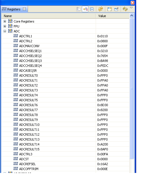
I am confused about how to a cascaded configured ADC with the DMA.  I tried all combinations of setting AdcRegs.ADCTRL2.bit.INT_ENA_SEQ1 and DmaRegs.CH5.MODE.bit.PERINTSEL. The code below shows the only configuration that allows the DMA to run somewhat, i.e. it only decrements the transfer count by 1 (from 15 to 14).  I included the DMA5 register image below.

Why isn't the DMA running to completion?

Stephen 

CODE:

int main(void)
{

   DisableDog();

   InitProcessor();

   DMA_Init();

   InternalADC_Init();


   InternalADC_StartCapture();

   while (!InternalADC_DataReady())
   {
   };

   while (1)
   {
   };

   return 0;
}

Uint8 InternalADC_DataReady(void)
{
   return ADCdataReady;
}

void InternalADC_StartCapture(void)
{
   AdcRegs.ADCTRL2.bit.SOC_SEQ1 = 1;
}

void InternalADC_Init(void)

{

    Uint16 i;
 

   ADCdataReady = FALSE;

   for(i=0;i<16;i++)
   {
      InternalADCdata[i]=0;
   }
    
   EALLOW;
   // HSPCLK to ADC enabled
   SysCtrlRegs.PCLKCR0.bit.ADCENCLK = 1;  
  
   PieVectTable.DINTCH5 = &InternalADC_DMAwriteTransferComplete_ISR;
   EDIS;  
  
   AdcRegs.ADCTRL1.bit.RESET = 1;   // Reset the ADC

   asm(" RPT #22 || NOP");          // Must wait for ADC reset to take effect

   (*ADC_cal_func_ptr)();

   //--- Select the ADC reference
   AdcRegs.ADCREFSEL.bit.REF_SEL = 0; // 0=internal, 1=external

   //--- Power-up the ADC
   AdcRegs.ADCTRL3.all = 0;
   AdcRegs.ADCTRL3.bit.ADCBGRFDN = 3;
   AdcRegs.ADCTRL3.bit.ADCPWDN = 1;   // Power-up reference and main ADC
   AdcRegs.ADCTRL3.bit.ADCCLKPS = 13; // ADC Core Clock = HSPCLK/(26*(ADCTRL1[7]+1))
  
   DELAY_US(5000); // Wait 5ms before using the ADC 
  
   AdcRegs.ADCTRL1.all = 0x0000;
   AdcRegs.ADCTRL1.bit.ACQ_PS = 1;
   AdcRegs.ADCTRL1.bit.SEQ_CASC = 1;  // Sequencer are cascaded.

   //--- Configure the other ADC register
   // 16 channels will be converted
   AdcRegs.ADCMAXCONV.all = INT_ADC_NUMBER_OF_CHANNELS-1;
     
   AdcRegs.ADCCHSELSEQ1.bit.CONV00 = 0;
   AdcRegs.ADCCHSELSEQ1.bit.CONV01 = 1;
   AdcRegs.ADCCHSELSEQ1.bit.CONV02 = 2;
   AdcRegs.ADCCHSELSEQ1.bit.CONV03 = 3;

   AdcRegs.ADCCHSELSEQ2.bit.CONV04 = 4;
   AdcRegs.ADCCHSELSEQ2.bit.CONV05 = 5;
   AdcRegs.ADCCHSELSEQ2.bit.CONV06 = 6;
   AdcRegs.ADCCHSELSEQ2.bit.CONV07 = 7;

   AdcRegs.ADCCHSELSEQ3.bit.CONV08 = 8;
   AdcRegs.ADCCHSELSEQ3.bit.CONV09 = 9;
   AdcRegs.ADCCHSELSEQ3.bit.CONV10 = 10;
   AdcRegs.ADCCHSELSEQ3.bit.CONV11 = 11;

   AdcRegs.ADCCHSELSEQ4.bit.CONV12 = 12;
   AdcRegs.ADCCHSELSEQ4.bit.CONV13 = 13;
   AdcRegs.ADCCHSELSEQ4.bit.CONV14 = 14;
   AdcRegs.ADCCHSELSEQ4.bit.CONV15 = 15;

#if (INT_ADC_NUMBER_OF_CHANNELS >= 8)
   AdcRegs.ADCTRL2.bit.INT_ENA_SEQ1 = 1;
#elif
   AdcRegs.ADCTRL2.bit.INT_ENA_SEQ1 = 1;
#endif
  
   PieCtrlRegs.PIEIER7.bit.INTx5 = 1;// Enable PIE Group 7, INT 5 (DMA CH5)

   DMAInitialize(); 
  
   EALLOW;
   DmaRegs.CH5.BURST_SIZE.all = 0;     // 1 word/burst
   DmaRegs.CH5.SRC_BURST_STEP = 1;     // increment 1 16-bit addr. btwn words
   DmaRegs.CH5.DST_BURST_STEP = 1;     // increment 1 16-bit addr. btwn words
   DmaRegs.CH5.TRANSFER_SIZE = INT_ADC_NUMBER_OF_CHANNELS-1;      // Interrupt every 16 bursts/transfer
   DmaRegs.CH5.SRC_TRANSFER_STEP = 1;   // Move to next word in buffer after each word in a burst
   DmaRegs.CH5.DST_TRANSFER_STEP = 1;   // Go back to AdcRegs.ADCRESULT0
   DmaRegs.CH5.SRC_ADDR_SHADOW = (Uint32) &AdcRegs.ADCRESULT0;
   DmaRegs.CH5.SRC_BEG_ADDR_SHADOW = (Uint32) &AdcRegs.ADCRESULT0;
   DmaRegs.CH5.DST_ADDR_SHADOW = (Uint32) &InternalADCdata[0];
   DmaRegs.CH5.DST_BEG_ADDR_SHADOW = (Uint32) &InternalADCdata[0];
   DmaRegs.CH5.CONTROL.bit.SYNCCLR = 1;      // Clear sync flag
   DmaRegs.CH5.CONTROL.bit.ERRCLR = 1; // Clear sync error flag
   DmaRegs.CH5.DST_WRAP_SIZE = 0xFFFF; // Put to maximum - don't want destination wrap
   DmaRegs.CH5.SRC_WRAP_SIZE = 0xFFFF; // Put to maximum - don't want source wrap
   DmaRegs.CH5.MODE.bit.SYNCE = 0;              // No sync signal
   DmaRegs.CH5.MODE.bit.SYNCSEL = 0;            // No sync signal
   DmaRegs.CH5.MODE.bit.CHINTE = 1;       // Enable channel interrupt
   DmaRegs.CH5.MODE.bit.CHINTMODE = 1;    // Interrupt at end of transfer
   DmaRegs.CH5.MODE.bit.PERINTE = 1;      // Enable peripheral interrupt event
   DmaRegs.CH5.MODE.bit.PERINTSEL = DMA_SEQ1INT; // Peripheral interrupt select = DMA_SEQ1INT
   DmaRegs.CH5.CONTROL.bit.PERINTCLR = 1; // Clear any spurious interrupt flags
   DmaRegs.CH5.MODE.bit.DATASIZE = 0;
   DmaRegs.CH5.CONTROL.bit.RUN = 1;
   EDIS;

   IER |= M_INT7 ;

}

  • Hello,

    Is any more information needed to help me with this issue.

    Thanks,
    Stephen

  • Hello,

    The main question is how do I set up a cascaded ADC and the DMA to transfer all 16 registers from the ADC to memory?  What am I doing wrong?

    Stephen

  • I have attached a CCS 5.3 test program.

    Please help.

    Thank,

    Stephen

    2555.testInternalADC.zip

  • Ok, I fixed my code a little. 

    By changing the DMA burst and transfer settings as shown below, the DMA registers show that it transferred 8 words before the DMA interrupt happens.  Shouldn't all the 16 channels get transferred?

    I also noticed that the InternalADCdata[] contains all zeros, which is different than what is show in the ADC register debug window.  I have attached both the DMA register window and the expression windows showing InternalADCdata[].

    If I change from enabling the SEQ1 interrupt to enabling the SEQ2 interrupt ( INT_ENA_SEQ2 = 1) and setting DmaRegs.CH5.MODE.bit.PERINTSEL = DMA_SEQ2INT, the DMA doesn't start the transfer.

    Can someone tell me what I am doing wrong.

    Thanks,

    Stephen

    From:

       DmaRegs.CH5.BURST_SIZE.all = 0;     // 1 word/burst
       DmaRegs.CH5.SRC_BURST_STEP = 1;     // increment 1 16-bit addr. btwn words
       DmaRegs.CH5.DST_BURST_STEP = 1;     // increment 1 16-bit addr. btwn words
       DmaRegs.CH5.TRANSFER_SIZE = INT_ADC_NUMBER_OF_CHANNELS-1;      // Interrupt every 16 bursts/transfer
       DmaRegs.CH5.SRC_TRANSFER_STEP = 1;   // Move to next word in buffer after each word in a burst
       DmaRegs.CH5.DST_TRANSFER_STEP = 1;   // Go back to AdcRegs.ADCRESULT0

    To:

       DmaRegs.CH5.BURST_SIZE.all = INT_ADC_NUMBER_OF_CHANNELS-1;     // 1 word/burst
       DmaRegs.CH5.SRC_BURST_STEP = 1;    // increment 1 16-bit addr. btwn words
       DmaRegs.CH5.DST_BURST_STEP = 1;     // increment 1 16-bit addr. btwn words
       DmaRegs.CH5.TRANSFER_SIZE = 0;      // Interrupt every 16 bursts/transfer
       DmaRegs.CH5.SRC_TRANSFER_STEP = 0;   // Move to next word in buffer after each word in a burst
       DmaRegs.CH5.DST_TRANSFER_STEP = 0;   // Go back to AdcRegs.ADCRESULT0


  • Stevenh,

    I have modified the ADCtoDMA example that is provided with controlSUITE and I it was successful at transferring 16 data samples. A few notes about the changes. I first changed to Cascaded Sequencer:

    AdcRegs.ADCTRL1.bit.SEQ_CASC = 1;        // 1 Cascaded Mode

    Next I added the extra conversion registers and changed max conversion for 16 conversions:

    AdcRegs.ADCCHSELSEQ1.bit.CONV00 = 0x0;

    AdcRegs.ADCCHSELSEQ1.bit.CONV01 = 0x1;

    AdcRegs.ADCCHSELSEQ1.bit.CONV02 = 0x2;

    AdcRegs.ADCCHSELSEQ1.bit.CONV03 = 0x3;

    AdcRegs.ADCCHSELSEQ2.bit.CONV04 = 0x4;

    AdcRegs.ADCCHSELSEQ2.bit.CONV05 = 0x5;

    AdcRegs.ADCCHSELSEQ2.bit.CONV06 = 0x6;

    AdcRegs.ADCCHSELSEQ2.bit.CONV07 = 0x7;

    AdcRegs.ADCCHSELSEQ3.bit.CONV08 = 0x8;

    AdcRegs.ADCCHSELSEQ3.bit.CONV09 = 0x9;

    AdcRegs.ADCCHSELSEQ3.bit.CONV10 = 0xA;

    AdcRegs.ADCCHSELSEQ3.bit.CONV11 = 0xB;

    AdcRegs.ADCCHSELSEQ4.bit.CONV12 = 0xC;

    AdcRegs.ADCCHSELSEQ4.bit.CONV13 = 0xD;

    AdcRegs.ADCCHSELSEQ4.bit.CONV14 = 0xE;

    AdcRegs.ADCCHSELSEQ4.bit.CONV15 = 0xF;

    AdcRegs.ADCMAXCONV.bit.MAX_CONV1 = 15;   // Set up ADC to perform 16 conversions for every SOC

    These were the only changes I made to the ADC configuration. For the DMA configuration, I needed to change the Burst, Transfer, and Wrap configurations:

    DMACH1BurstConfig(15,1,1);

    DMACH1TransferConfig(1,0,15);

    DMACH1WrapConfig(100,0,0,100);

    The burst config is for 16 data points and increments SRC and DEST by 1 address. The Transfer config is for 1 Burst, no increment of source, and 16 byte increment Dest. Wrap is disabled by writing a higher number than transfer.

    The last thing I changed for the DMA is when the interrupt is produced. I changed this to happen at the beginning of the Transfer:

    DMACH1ModeConfig(DMA_SEQ1INT,PERINT_ENABLE,ONESHOT_DISABLE,CONT_DISABLE,SYNC_DISABLE,SYNC_SRC, OVRFLOW_DISABLE,SIXTEEN_BIT,CHINT_BEGIN,CHINT_ENABLE);


    With this configuration you can free run and you will halt at the ESTOP command in the DMA interrupt. You can then compare ADC Result Regs with DMABuf1 and you will see that the transfer occurred. I have included those screenshots below. Also below is the Example_2833xAdcToDMA.c file. You can use this to test in the adctodma example provided in the C:\ti\controlSUITE\device_support\f2833x directory of controlSUITE.

    //###########################################################################
    //
    // FILE:   Example_2833xAdcToDMA.c
    //
    // TITLE:  DSP2833x ADC To DMA
    // ASSUMPTIONS:
    //
    //    This program requires the DSP2833x header files.
    //
    //    Make sure the CPU clock speed is properly defined in
    //    DSP2833x_Examples.h before compiling this example.
    //
    //    Connect the signals to be converted to channel A0, A1, A2, and A3.
    //
    //    As supplied, this project is configured for "boot to SARAM"
    //    operation.  The 2833x Boot Mode table is shown below.
    //    For information on configuring the boot mode of an eZdsp,
    //    please refer to the documentation included with the eZdsp,
    //
    //       $Boot_Table:
    //
    //         GPIO87   GPIO86     GPIO85   GPIO84
    //          XA15     XA14       XA13     XA12
    //           PU       PU         PU       PU
    //        ==========================================
    //            1        1          1        1    Jump to Flash
    //            1        1          1        0    SCI-A boot
    //            1        1          0        1    SPI-A boot
    //            1        1          0        0    I2C-A boot
    //            1        0          1        1    eCAN-A boot
    //            1        0          1        0    McBSP-A boot
    //            1        0          0        1    Jump to XINTF x16
    //            1        0          0        0    Jump to XINTF x32
    //            0        1          1        1    Jump to OTP
    //            0        1          1        0    Parallel GPIO I/O boot
    //            0        1          0        1    Parallel XINTF boot
    //            0        1          0        0    Jump to SARAM	    <- "boot to SARAM"
    //            0        0          1        1    Branch to check boot mode
    //            0        0          1        0    Boot to flash, bypass ADC cal
    //            0        0          0        1    Boot to SARAM, bypass ADC cal
    //            0        0          0        0    Boot to SCI-A, bypass ADC cal
    //                                              Boot_Table_End$
    //
    //
    // DESCRIPTION:
    //
    // ADC is setup to convert 4 channels for each SOC received, with  total of 10 SOCs.
    // Each SOC initiates 4 conversions.
    // DMA is set up to capture the data on each SEQ1_INT.  DMA will re-sort   
    // the data by channel sequentially, i.e. all channel0 data will be together
    // all channel1 data will be together.
    //
    // Code should stop in local_DINTCH1_ISR when complete
    //
    // Watch Variables:
    //      DMABuf1
    //
    //###########################################################################
    //
    // Original source by: M.P.
    //
    // $TI Release: 2833x/2823x Header Files V1.32 $
    // $Release Date: June 28, 2010 $
    //###########################################################################
    
    #include "DSP28x_Project.h"     // Device Headerfile and Examples Include File
    
    // ADC start parameters
    #if (CPU_FRQ_150MHZ)     // Default - 150 MHz SYSCLKOUT
      #define ADC_MODCLK 0x3 // HSPCLK = SYSCLKOUT/2*ADC_MODCLK2 = 150/(2*3)   = 25.0 MHz
    #endif
    #if (CPU_FRQ_100MHZ)
      #define ADC_MODCLK 0x2 // HSPCLK = SYSCLKOUT/2*ADC_MODCLK2 = 100/(2*2)   = 25.0 MHz
    #endif
    #define ADC_CKPS   0x1   // ADC module clock = HSPCLK/2*ADC_CKPS   = 25.0MHz/(1*2) = 12.5MHz
    #define ADC_SHCLK  0xf   // S/H width in ADC module periods                        = 16 ADC clocks
    #define AVG        1000  // Average sample limit
    #define ZOFFSET    0x00  // Average Zero offset
    #define BUF_SIZE   40    // Sample buffer size
    
    // Global variable for this example
    Uint16 j=0;
    
    #pragma DATA_SECTION(DMABuf1,"DMARAML4");
    volatile Uint16 DMABuf1[40];
    
    volatile Uint16 *DMADest;
    volatile Uint16 *DMASource;
    interrupt void local_DINTCH1_ISR(void);
    
    void main(void)
    {
       Uint16 i;
    // Step 1. Initialize System Control:
    // PLL, WatchDog, enable Peripheral Clocks
    // This example function is found in the DSP2833x_SysCtrl.c file.
       InitSysCtrl();
    
    // Specific clock setting for this example:
       EALLOW;
       SysCtrlRegs.HISPCP.all = ADC_MODCLK;	// HSPCLK = SYSCLKOUT/ADC_MODCLK
       EDIS;
    
    // Step 2. Initialize GPIO:
    // This example function is found in the DSP2833x_Gpio.c file and
    // illustrates how to set the GPIO to it's default state.
    // InitGpio();  // Skipped for this example
    
    // Step 3. Clear all interrupts and initialize PIE vector table:
    // Disable CPU interrupts
       DINT;
    
    // Initialize the PIE control registers to their default state.
    // The default state is all PIE interrupts disabled and flags
    // are cleared.
    // This function is found in the DSP2833x_PieCtrl.c file.
       InitPieCtrl();
    
    // Disable CPU interrupts and clear all CPU interrupt flags:
       IER = 0x0000;
       IFR = 0x0000;
    
    // Initialize the PIE vector table with pointers to the shell Interrupt
    // Service Routines (ISR).
    // This will populate the entire table, even if the interrupt
    // is not used in this example.  This is useful for debug purposes.
    // The shell ISR routines are found in DSP2833x_DefaultIsr.c.
    // This function is found in DSP2833x_PieVect.c.
       InitPieVectTable();
    
    // Interrupts that are used in this example are re-mapped to
    // ISR functions found within this file.
       EALLOW;	// Allow access to EALLOW protected registers
       PieVectTable.DINTCH1= &local_DINTCH1_ISR;
       EDIS;   // Disable access to EALLOW protected registers
          
       IER = M_INT7 ;	                             //Enable INT7 (7.1 DMA Ch1)
       EnableInterrupts();
       
    // Step 4. Initialize all the Device Peripherals:
    // This function is found in DSP2833x_InitPeripherals.c
    // InitPeripherals(); // Not required for this example
       InitAdc();  // For this example, init the ADC
    
    // Specific ADC setup for this example:
       AdcRegs.ADCTRL1.bit.ACQ_PS = ADC_SHCLK;
       AdcRegs.ADCTRL3.bit.ADCCLKPS = ADC_CKPS;
       AdcRegs.ADCTRL1.bit.SEQ_CASC = 1;        // 1 Cascaded Mode
       AdcRegs.ADCTRL2.bit.INT_ENA_SEQ1 = 0x1;
       AdcRegs.ADCTRL2.bit.RST_SEQ1 = 0x1;
       AdcRegs.ADCCHSELSEQ1.bit.CONV00 = 0x0;
       AdcRegs.ADCCHSELSEQ1.bit.CONV01 = 0x1;
       AdcRegs.ADCCHSELSEQ1.bit.CONV02 = 0x2;
       AdcRegs.ADCCHSELSEQ1.bit.CONV03 = 0x3;
       AdcRegs.ADCCHSELSEQ2.bit.CONV04 = 0x4;
       AdcRegs.ADCCHSELSEQ2.bit.CONV05 = 0x5;
       AdcRegs.ADCCHSELSEQ2.bit.CONV06 = 0x6;
       AdcRegs.ADCCHSELSEQ2.bit.CONV07 = 0x7;
       AdcRegs.ADCCHSELSEQ3.bit.CONV08 = 0x8;
       AdcRegs.ADCCHSELSEQ3.bit.CONV09 = 0x9;
       AdcRegs.ADCCHSELSEQ3.bit.CONV10 = 0xA;
       AdcRegs.ADCCHSELSEQ3.bit.CONV11 = 0xB;
    
       AdcRegs.ADCCHSELSEQ4.bit.CONV12 = 0xC;
       AdcRegs.ADCCHSELSEQ4.bit.CONV13 = 0xD;
       AdcRegs.ADCCHSELSEQ4.bit.CONV14 = 0xE;
       AdcRegs.ADCCHSELSEQ4.bit.CONV15 = 0xF;
       AdcRegs.ADCMAXCONV.bit.MAX_CONV1 = 15;   // Set up ADC to perform 16 conversions for every SOC
       
    //Step 5. User specific code, enable interrupts:
      // Initialize DMA 
    	DMAInitialize();
    
    	// Clear Table
       for (i=0; i<BUF_SIZE; i++)
       {
         DMABuf1[i] = 0;
       }
    
    	
    // Configure DMA Channel
        DMADest   = &DMABuf1[0];              //Point DMA destination to the beginning of the array
    	DMASource = &AdcMirror.ADCRESULT0;    //Point DMA source to ADC result register base
    	DMACH1AddrConfig(DMADest,DMASource);
    	DMACH1BurstConfig(15,1,1);
    	DMACH1TransferConfig(1,0,15);
    	DMACH1WrapConfig(100,0,0,100);
    	DMACH1ModeConfig(DMA_SEQ1INT,PERINT_ENABLE,ONESHOT_DISABLE,CONT_DISABLE,SYNC_DISABLE,SYNC_SRC,
    	                 OVRFLOW_DISABLE,SIXTEEN_BIT,CHINT_BEGIN,CHINT_ENABLE);
    
    	StartDMACH1();
    
       // Start SEQ1
       AdcRegs.ADCTRL2.bit.SOC_SEQ1 = 0x1;
       while(1);
    }
    
    // INT7.1
    interrupt void local_DINTCH1_ISR(void)     // DMA Channel 1
    {
      
      // To receive more interrupts from this PIE group, acknowledge this interrupt 
       PieCtrlRegs.PIEACK.all = PIEACK_GROUP7;
    
      // Next two lines for debug only to halt the processor here
      // Remove after inserting ISR Code
       asm ("      ESTOP0");
       for(;;);
    }


    Regards,

    Tim Love

  • Here are the screenshots.

  • Tim,

    I tried building your modified code and get these errors:

    Description Resource Path Location Type
    errors encountered during linking; "Example_2833xAdcToDMA.out" not Example_2833xAdcToDMA    C/C++ Problem
    unresolved symbols remain Example_2833xAdcToDMA    C/C++ Problem
    unresolved symbol _main, first referenced in C:/ti/ccsv5/tools/compiler/c2000_6.1.0/lib/rts2800_fpu32.lib<args_main.obj> Example_2833xAdcToDMA    C/C++ Problem
    cannot find file "rts2800_fpu32_fast_supplement.lib" Example_2833xAdcToDMA    C/C++ Problem

    I am using Code Composer v5.3 with the F28335 experimenter's kit.

    -Chuck

  • Thanks Tim,

    After looking at your attached c file and playing around with my project, I was able to get it to work if I only change &AdcRegs.ADCRESULT0 to &AdcMirror.ADCRESULT0 in my project.

    It looks like there's an issue with the DMA using the ADC Peripheral Frame 2.  Is it because of the wait states?

    Stephen

    Stephen

  • Chuck,

    This example was written a while back and there is a Fast RTS library included that is no longer in the controlSUITE package. You can remove this file by right clicking on the project and selecting Properties. Now on the left side of the properties you will see several options. Under C2000 Linker you will see File Search Path. Click on this option. Here you will see 3 libraries listed up top including the fast_supplement.lib causing the error. From here you can simply use the delete option and remove this library. After this, it should build properly.

    Regards,

    Tim Love

  • Tim,

    I did what you recommended and now I get three errors instead of four:

    Description Resource Path Location Type
    errors encountered during linking; "Example_2833xAdcToDMA.out" not Example_2833xAdcToDMA    C/C++ Problem
    unresolved symbols remain Example_2833xAdcToDMA    C/C++ Problem
    unresolved symbol _main, first referenced in C:/ti/ccsv5/tools/compiler/c2000_6.1.0/lib/rts2800_fpu32.lib<args_main.obj> Example_2833xAdcToDMA    C/C++ Problem

    -Chuck

  • Stephen,

    You are correct that there is an issue with accessing the registers in Peripheral Frame 2. Internally, the registers that are accessible by the DMA are contained in Peripheral Frame 0. You can see the following information on page 32 of the ADC Reference Guide (SPRU812):

    The ADC result registers located in peripheral frame 0 (0x0B00 – 0x0B0F) are accessible by the DMA unit on the F2833x.

    Regards,

    Tim Love

  • Chuck,

    Did you remove rts2800_fpu32.lib? If so, that is not the one to delete. The one to delete ended with fast_supplement.lib. You need rts2800_fpu32.lib as this establishes the C environment, initializes variables, contains rts functions, etc.

    Regards,

    Tim Love

  • Thanks.  prior to seeing your code I actually didn't realize there were two buffers locations.

    Thanks,

    Stephen

  • Tim,

    No, I removed fast_supplement.lib

    -Chuck

  • Charles,

    You'll be able to use my previously attached project with the changes shown in this thread and it should work. The project is a CCSv5.3 version project.

    Stephen

  • Tim,

    For some reason, I cannot get the project to build without errors. I commented out the modifications and uncommented the original code

    and I still get three errors when building. I've tried cleaning the project and reloading it but still errors. Can you email me a fresh copy of the example project?

    charles.jackel@esterline.com

    Thanks,

    Chuck

  • Tim,

     I can't get the project to build without these 3 errors:

    1. errors encountered during linking; "Example_2833xAdcToDMA.out" not 
    2. unresolved symbol _main, first referenced in C:/ti/ccsv5/tools/compiler/c2000_6.1.0/lib/rts2800_fpu32.lib<args_main.obj> 
    3. unresolved symbols remain 

    I did a clean install of Code Composer v5.3 and controlSUITE but still get these errors. The previously Fast library you said to delete is not in the file path directory. 

    I can build and debug the example ADC_soc project with no problem. Any thoughts why I keep getting these errors?

    -Chuck