This thread has been locked.

If you have a related question, please click the "Ask a related question" button in the top right corner. The newly created question will be automatically linked to this question.

Questions about SPI Initialization

Other Parts Discussed in Thread: CCSTUDIO

Greetings,

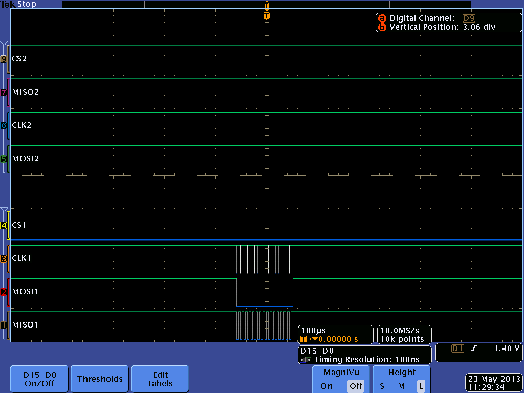
I am using the F28335 and I am not sure if I am initializing the SPI correctly to work for gpio ports 12,13, 14, and 15.  Is this the correct way to do it?  I can't seem to see any signals being sent out from these pins.  

case 3:
if (strncmp(SPI_Mode, "MOSI",4)== 0){
// SciaTx("GPIO12");
GpioCtrlRegs.GPAPUD.bit.GPIO12 = 0; // Enable pull-up on GPIO12 (SPISIMOA)
GpioCtrlRegs.GPAQSEL1.bit.GPIO12 = 3; // Asynch input GPIO12 (SPISIMOA)
GpioCtrlRegs.GPAMUX1.bit.GPIO12 = 1; // Configure GPIO12 as SPISIMOA
GpioCtrlRegs.GPADIR.bit.GPIO12 = 1; //set FRAM CS as out
}

else if (strncmp(SPI_Mode, "MISO",4)== 0){
// SciaTx("GPIO12");
GpioCtrlRegs.GPAPUD.bit.GPIO13 = 0; // Enable pull-up on GPIO13 (SPISOMIA)
GpioCtrlRegs.GPAQSEL1.bit.GPIO13 = 3; // Asynch input GPIO13 (SPISOMIA)
GpioCtrlRegs.GPAMUX1.bit.GPIO13 = 1; // Configure GPIO13 as SPISOMIA 
}

else if (strncmp(SPI_Mode, "CLK=",4)== 0){

// SciaTx("GPIO14");
GpioCtrlRegs.GPAPUD.bit.GPIO14 = 0; // Enable pull-up on GPIO14 (SPICLKA)
GpioCtrlRegs.GPAQSEL1.bit.GPIO14 = 3; // Asynch input GPIO14 (SPICLKA)
GpioCtrlRegs.GPAMUX1.bit.GPIO14 = 1; // Configure GPIO14 as SPICLKA
GpioCtrlRegs.GPADIR.bit.GPIO14 = 1; //set FRAM CS as out
}

else if (strncmp(SPI_Mode, "CS=G",4)== 0){
// SciaTx("GPIO15");
GpioDataRegs.GPASET.bit.GPIO15 = 1; //pre-set FRAM CS high
GpioCtrlRegs.GPADIR.bit.GPIO15 = 1; //set FRAM CS as out 
}

  • David,

    A quick thought: make sure you have executed an EALLOW.  The GpioCtrlRegs are EALLOW protected.  If you don't execute the EALLOW, your code will not actually configure the registers.

    - David

  • I do call Eallow before I initialize the function.  The code I attached was just a portion of the function here is the full functions.


    void InitSpiaGpio(char SPIcase[], char SPI_Mode[], Uint16 mode)
    {
    struct ECAN_REGS;


    EALLOW;

    switch (mode){

    case 1:

    if (strncmp(SPI_Mode, "MOSI",4)== 0)
    {
    if(SPIcase[0]=='5' && SPIcase[1]=='4')
    {
    // SciaTx("GPIO54");
    GpioCtrlRegs.GPBPUD.bit.GPIO54 = 0; // Enable pull-up on GPIO54 (SPISIMOA)
    GpioCtrlRegs.GPBQSEL2.bit.GPIO54 = 3; // Asynch input GPIO54 (SPISIMOA)
    GpioCtrlRegs.GPBMUX2.bit.GPIO54 = 1; // Configure GPIO54 as SPISIMOA
    GpioCtrlRegs.GPBDIR.bit.GPIO54 = 1; //set FRAM CS as out
    }

    else if(SPIcase[0]=='1' && SPIcase[1]=='6')
    {
    // SciaTx("GPIO16");
    GpioCtrlRegs.GPAPUD.bit.GPIO16 = 0; // Enable pull-up on GPIO16 (SPISIMOA)
    GpioCtrlRegs.GPAQSEL2.bit.GPIO16 = 3; // Asynch input GPIO16 (SPISIMOA)
    GpioCtrlRegs.GPAMUX2.bit.GPIO16 = 1; // Configure GPIO16 as SPISIMOA
    GpioCtrlRegs.GPADIR.bit.GPIO16 = 1; //set FRAM CS as out

    }
    }

    else if (strncmp(SPI_Mode, "MISO",4)== 0)
    {

    if(SPIcase[0]=='5' && SPIcase[1]=='5')
    {
    // SciaTx("GPIO55");
    GpioCtrlRegs.GPBPUD.bit.GPIO55 = 0; // Enable pull-up on GPIO54 (SPISIMOA)
    GpioCtrlRegs.GPBQSEL2.bit.GPIO55 = 3; // Asynch input GPIO55 (SPISOMIA)
    GpioCtrlRegs.GPBMUX2.bit.GPIO55 = 1; // Configure GPIO55 as SPISOMIA
    }

    else if(SPIcase[0]=='1' && SPIcase[1]=='7')
    {
    // SciaTx("GPIO17");
    GpioCtrlRegs.GPAPUD.bit.GPIO17 = 0; // Enable pull-up on GPIO17 (SPISOMIA)
    GpioCtrlRegs.GPAQSEL2.bit.GPIO17 = 3; // Asynch input GPIO17 (SPISOMIA)
    GpioCtrlRegs.GPAMUX2.bit.GPIO17 = 1; // Configure GPIO17 as SPISOMIA
    }
    }

    else if (strncmp(SPI_Mode, "CLK=",4)== 0)
    {

    if(SPIcase[0]=='5' && SPIcase[1]=='6')
    {
    // SciaTx("GPIO56");
    GpioCtrlRegs.GPBPUD.bit.GPIO56 = 0; // Enable pull-up on GPIO56 (SPICLKA)
    GpioCtrlRegs.GPBQSEL2.bit.GPIO56 = 3; // Asynch input GPIO56 (SPICLKA)
    GpioCtrlRegs.GPBMUX2.bit.GPIO56 = 1; // Configure GPIO56 as SPICLKA
    GpioCtrlRegs.GPBDIR.bit.GPIO56 = 1; //set FRAM CS as out
    }

    else if(SPIcase[0]=='1' && SPIcase[1]=='8')
    {
    // SciaTx("GPIO18");
    GpioCtrlRegs.GPAPUD.bit.GPIO18 = 0; // Enable pull-up on GPIO18 (SPICLKA)
    GpioCtrlRegs.GPAQSEL2.bit.GPIO18 = 3; // Asynch input GPIO18 (SPICLKA)
    GpioCtrlRegs.GPAMUX2.bit.GPIO18 = 1; // Configure GPIO18 as SPICLKA
    GpioCtrlRegs.GPADIR.bit.GPIO18 = 1; //set FRAM CS as out
    }
    }

    else if (strncmp(SPI_Mode, "CS=G",4)== 0)
    {
    if(SPIcase[0]=='5' && SPIcase[1]=='7')
    {
    // SciaTx("GPIO57");
    GpioDataRegs.GPBSET.bit.GPIO57 = 1; //pre-set FRAM CS high
    GpioCtrlRegs.GPBDIR.bit.GPIO57 = 1; //set FRAM CS as out
    // GpioDataRegs.GPBSET.bit.GPIO58 = 1; //pre-set EEP CS high
    // GpioCtrlRegs.GPBDIR.bit.GPIO58 = 1; //set EEP CS as out
    }

    else if(SPIcase[0]=='1' && SPIcase[1]=='9')
    {
    // SciaTx("GPIO19");
    GpioDataRegs.GPASET.bit.GPIO19 = 1; //pre-set FRAM CS high
    GpioCtrlRegs.GPADIR.bit.GPIO19 = 1; //set FRAM CS as out
    }
    }
    break;

    case 2:

    if (strncmp(SPI_Mode, "MOSI",4)== 0){
    // SciaTx("GPIO20");
    GpioCtrlRegs.GPAPUD.bit.GPIO20 = 0; // Enable pull-up on GPIO20 (SPISIMOA)
    GpioCtrlRegs.GPAQSEL2.bit.GPIO20 = 3; // Asynch input GPIO20 (SPISIMOA)
    GpioCtrlRegs.GPAMUX2.bit.GPIO20 = 1; // Configure GPIO20 as SPISIMOA
    GpioCtrlRegs.GPADIR.bit.GPIO20 = 1; //set FRAM CS as out
    }

    else if (strncmp(SPI_Mode, "MISO",4)== 0){
    // SciaTx("GPIO21");
    GpioCtrlRegs.GPAPUD.bit.GPIO21 = 0; // Enable pull-up on GPIO21 (SPISOMIA)
    GpioCtrlRegs.GPAQSEL2.bit.GPIO21 = 3; // Asynch input GPIO21 (SPISOMIA)
    GpioCtrlRegs.GPAMUX2.bit.GPIO21 = 1; // Configure GPIO21 as SPISOMIA
    }

    else if (strncmp(SPI_Mode, "CLK=",5)== 0){
    // SciaTx("GPIO22");
    GpioCtrlRegs.GPAPUD.bit.GPIO22 = 0; // Enable pull-up on GPIO22 (SPICLKA)
    GpioCtrlRegs.GPAQSEL2.bit.GPIO22 = 3; // Asynch input GPIO22 (SPICLKA)
    GpioCtrlRegs.GPAMUX2.bit.GPIO22 = 1; // Configure GPIO22 as SPICLKA
    GpioCtrlRegs.GPADIR.bit.GPIO22 = 1; //set FRAM CS as out
    }

    else if (strncmp(SPI_Mode, "CS=G",4)== 0){
    // SciaTx("GPIO23");
    GpioDataRegs.GPASET.bit.GPIO23 = 1; //pre-set FRAM CS high
    GpioCtrlRegs.GPADIR.bit.GPIO23 = 1; //set FRAM CS as out
    }

    break;

    case 3:
    if (strncmp(SPI_Mode, "MOSI",4)== 0){
    // SciaTx("GPIO11");
    GpioCtrlRegs.GPAPUD.bit.GPIO12 = 0; // Enable pull-up on GPIO12 (SPISIMOA)
    GpioCtrlRegs.GPAQSEL1.bit.GPIO12 = 3; // Asynch input GPIO12 (SPISIMOA)
    GpioCtrlRegs.GPAMUX1.bit.GPIO12 = 1; // Configure GPIO12 as SPISIMOA
    GpioCtrlRegs.GPADIR.bit.GPIO12 = 1; //set FRAM CS as out
    }

    else if (strncmp(SPI_Mode, "MISO",4)== 0){
    // SciaTx("GPIO12");
    GpioCtrlRegs.GPAPUD.bit.GPIO13 = 0; // Enable pull-up on GPIO13 (SPISOMIA)
    GpioCtrlRegs.GPAQSEL1.bit.GPIO13 = 3; // Asynch input GPIO13 (SPISOMIA)
    GpioCtrlRegs.GPAMUX1.bit.GPIO13 = 1; // Configure GPIO13 as SPISOMIA
    }

    else if (strncmp(SPI_Mode, "CLK=",4)== 0){

    // SciaTx("GPIO14");
    GpioCtrlRegs.GPAPUD.bit.GPIO14 = 0; // Enable pull-up on GPIO14 (SPICLKA)
    GpioCtrlRegs.GPAQSEL1.bit.GPIO14 = 3; // Asynch input GPIO14 (SPICLKA)
    GpioCtrlRegs.GPAMUX1 .bit.GPIO14 = 1; // Configure GPIO15 as SPICLKA
    GpioCtrlRegs.GPADIR.bit.GPIO14 = 1; //set FRAM CS as out
    }

    else if (strncmp(SPI_Mode, "CS=G",4)== 0){
    // SciaTx("GPIO15");
    GpioDataRegs.GPASET.bit.GPIO15 = 1; //pre-set FRAM CS high
    GpioCtrlRegs.GPADIR.bit.GPIO15 = 1; //set FRAM CS as out
    }

    break;
    }
    EDIS;
    }

  • David,

    Are you trying to use SPI-A, or McBSP-A in SPI mode?  GPIO pins 12-15 are for McBSP-A, not SPI-A.

    - David

  • I need to do the McBSP (a).  How would I initialize the ports for McBSP-A?

  • David,

    I need to correct myself.  GPIO12-15 are for McBSP-B.  McBSP-A is on GPIO20-23, and also a couple of the signals also come out on GPIO5, 7, 58, and 59.


    So, are you sure you are using the correct pins?

    - David

  • Then I guess is McBSP-B I need.  Is there anything different I need to do to initialize ports12-15?

  • There is nothing special about McBSP-B vs. McBSP-A.  The question I have is whether you are actually using McBSP-B in your code.  There seems to be some confusion here.  You are showing the GPIO configuration, but which McBSP port do you actually configure and use?

    - David

  • Can I just change all these values from McBSPA to McBSPB?

    void InitMcbspa(void)
    {
    // McBSP-A register settings
    McbspaRegs.SPCR2.all=0x0000; // Reset FS generator, sample rate generator & transmitter
    McbspaRegs.SPCR1.all=0x0000; // Reset Receiver, Right justify word, Digital loopback dis.
    McbspaRegs.PCR.all=0x0F08; //(CLKXM=CLKRM=FSXM=FSRM= 1, FSXP = 1)
    McbspaRegs.SPCR1.bit.CLKSTP = 3; // Together with CLKXP/CLKRP determines clocking scheme
    McbspaRegs.PCR.bit.CLKXP = 0; // CPOL = 0, CPHA = 0 rising edge no delay
    McbspaRegs.PCR.bit.CLKRP = 1;
    McbspaRegs.RCR2.bit.RDATDLY=01; // FSX setup time 1 in master mode. 0 for slave mode (Receive)
    McbspaRegs.XCR2.bit.XDATDLY=01; // FSX setup time 1 in master mode. 0 for slave mode (Transmit)

    McbspaRegs.RCR1.bit.RWDLEN1=0; // 8-bit word
    McbspaRegs.XCR1.bit.XWDLEN1=0; // 8-bit word
    McbspaRegs.XCR1.bit.XFRLEN1=0; //one word frame

    McbspaRegs.SRGR2.all=0x2000; // CLKSM=1, FPER = 1 CLKG periods
    McbspaRegs.SRGR1.all= 0x0009; // Frame Width = 1 CLKG period, CLKGDV=7


    delay_loop(); // Wait at least 2 SRG clock cycles

    McbspaRegs.SPCR2.bit.GRST=1; // Enable the sample rate generator
    clkg_delay_loop(); // Wait at least 2 CLKG cycles
    McbspaRegs.SPCR2.bit.XRST=1; // Release TX from Reset
    McbspaRegs.SPCR1.bit.RRST=1; // Release RX from Reset
    McbspaRegs.SPCR2.bit.FRST=1; // Frame Sync Generator reset

    }

  • I'd expect so.


  • I implemented the changes but it doesn't appear to work still.  Below is my code.  When I call the McBSP_Write00 it seems to get stuck at the first 

    while(McbspbRegs.SPCR2.bit.XRDY !=1)
    {}

    Can you help me see what i'm missing.  It never leaves this while loop.


    extern void DSP28x_usDelay(Uint32 Count);
    // For 150 MHz SYSCLKOUT(default)
    #define CPU_SPD 150E6
    #define MCBSP_SRG_FREQ CPU_SPD/4 // SRG input is LSPCLK (SYSCLKOUT/4) for examples


    #define CLKGDV_VAL 1
    #define MCBSP_INIT_DELAY 2*(CPU_SPD/MCBSP_SRG_FREQ) // # of CPU cycles in 2 SRG cycles-init delay
    #define MCBSP_CLKG_DELAY 2*(CPU_SPD/(MCBSP_SRG_FREQ/(1+CLKGDV_VAL))) // # of CPU cycles in 2 CLKG cycles-init delay
    #define SPIB_CS GpioDataRegs.GPADAT.bit.GPIO15
    #define SPIB_CLK GpioDataRegs.GPADAT.bit.GPIO14
    #define SPIB_DIN GpioDataRegs.GPADAT.bit.GPIO13
    #define SPIB_DOUT GpioDataRegs.GPADAT.bit.GPIO12
    //---------------------------------------------------------------------------
    // InitMcbsp:
    //---------------------------------------------------------------------------
    // This function initializes the McBSP to a known state.
    //

    void delay_loop(void); // Delay function used for SRG initialization
    void clkg_delay_loop(void); // Delay function used for CLKG initialization

    void InitMcbspb(void)
    {
    // McBSP-B register settings
    McbspbRegs.SPCR2.all=0x0000; // Reset FS generator, sample rate generator & transmitter
    McbspbRegs.SPCR1.all=0x0000; // Reset Receiver, Right justify word, Digital loopback dis.
    McbspbRegs.PCR.all=0x0F08; //(CLKXM=CLKRM=FSXM=FSRM= 1, FSXP = 1)
    McbspbRegs.SPCR1.bit.CLKSTP = 3; // Together with CLKXP/CLKRP determines clocking scheme
    McbspbRegs.PCR.bit.CLKXP = 0; // CPOL = 0, CPHA = 0 rising edge no delay
    McbspbRegs.PCR.bit.CLKRP = 1;
    McbspbRegs.RCR2.bit.RDATDLY=01; // FSX setup time 1 in master mode. 0 for slave mode (Receive)
    McbspbRegs.XCR2.bit.XDATDLY=01; // FSX setup time 1 in master mode. 0 for slave mode (Transmit)

    McbspbRegs.RCR1.bit.RWDLEN1=0; // 8-bit word
    McbspbRegs.XCR1.bit.XWDLEN1=0; // 8-bit word
    McbspbRegs.XCR1.bit.XFRLEN1=0; //one word frame

    McbspbRegs.SRGR2.all=0x2000; // CLKSM=1, FPER = 1 CLKG periods
    McbspbRegs.SRGR1.all= 0x0009; // Frame Width = 1 CLKG period, CLKGDV=7


    delay_loop(); // Wait at least 2 SRG clock cycles

    McbspbRegs.SPCR2.bit.GRST=1; // Enable the sample rate generator
    clkg_delay_loop(); // Wait at least 2 CLKG cycles
    McbspbRegs.SPCR2.bit.XRST=1; // Release TX from Reset
    McbspbRegs.SPCR1.bit.RRST=1; // Release RX from Reset
    McbspbRegs.SPCR2.bit.FRST=1; // Frame Sync Generator reset

    }

    // McBSP-B Data Lengths
    void InitMcbspb8bit(void)
    {
    McbspbRegs.RCR1.bit.RWDLEN1=0; // 8-bit word
    McbspbRegs.XCR1.bit.XWDLEN1=0; // 8-bit word

    }

    void InitMcbspbGpio(char SPIcase[], char SPI_Mode[])
    {

    EALLOW;

    if (strncmp(SPI_Mode, "MOSI",4)== 0){
    // SciaTx("GPIO11");
    GpioCtrlRegs.GPAPUD.bit.GPIO12 = 0; // Enable pull-up on GPIO12 (SPISIMOA)
    GpioCtrlRegs.GPAQSEL1.bit.GPIO12 = 3; // Asynch input GPIO12 (SPISIMOA)
    GpioCtrlRegs.GPAMUX1.bit.GPIO12 = 1; // Configure GPIO12 as SPISIMOA
    GpioCtrlRegs.GPADIR.bit.GPIO12 = 1; //set FRAM CS as out
    }

    else if (strncmp(SPI_Mode, "MISO",4)== 0){
    // SciaTx("GPIO12");
    GpioCtrlRegs.GPAPUD.bit.GPIO13 = 0; // Enable pull-up on GPIO13 (SPISOMIA)
    GpioCtrlRegs.GPAQSEL1.bit.GPIO13 = 3; // Asynch input GPIO13 (SPISOMIA)
    GpioCtrlRegs.GPAMUX1.bit.GPIO13 = 1; // Configure GPIO13 as SPISOMIA
    }

    else if (strncmp(SPI_Mode, "CLK=",4)== 0){

    // SciaTx("GPIO14");
    GpioCtrlRegs.GPAPUD.bit.GPIO14 = 0; // Enable pull-up on GPIO14 (SPICLKA)
    GpioCtrlRegs.GPAQSEL1.bit.GPIO14 = 3; // Asynch input GPIO14 (SPICLKA)
    GpioCtrlRegs.GPAMUX1 .bit.GPIO14 = 1; // Configure GPIO15 as SPICLKA
    GpioCtrlRegs.GPADIR.bit.GPIO14 = 1; //set FRAM CS as out
    }

    else if (strncmp(SPI_Mode, "CS=G",4)== 0){
    // SciaTx("GPIO15");
    GpioDataRegs.GPASET.bit.GPIO15 = 1; //pre-set FRAM CS high
    GpioCtrlRegs.GPADIR.bit.GPIO15 = 1; //set FRAM CS as out
    }

    EDIS;

    }

    void delay_loop(void)
    {
    long i;
    for (i = 0; i < MCBSP_INIT_DELAY; i++) {} //delay in McBsp init. must be at least 2 SRG cycles
    }

    void clkg_delay_loop(void)
    {
    long i;
    for (i = 0; i < MCBSP_CLKG_DELAY; i++) {} //delay in McBsp init. must be at least 2 SRG cycles
    }

    //---------------------------------------------------------------------------
    // McBSP_Write:
    //---------------------------------------------------------------------------
    // This function executes a write, mode 1, on the McBSP in SPI mode
    //
    // This will need to change to reflect the MAX1033 Chip message format
    //
    void McBSP_Write00(Uint16 CS, Uint16 *dp,Uint16 data_length){
    //---------------------------------------------------------------------------
    // #ifdef RELEASE
    Uint16 i;

    InitMcbspb8bit();
    SPIB_CS = 0;
    for(i=0;i<data_length;i++){
    while(McbspbRegs.SPCR2.bit.XRDY !=1)
    {}
    McbspbRegs.DXR1.all = *dp++;
    }
    while(McbspbRegs.SPCR2.bit.XRDY !=1)
    {}
    while(McbspbRegs.SPCR2.bit.XEMPTY ==1)
    {}
    DELAY_US(5);
    SPIB_CS = 1;
    SciaTxByte(data_length);
    //#endif
    }

  • David,

    I wrote you a simple example that works.  It is only doing transmit, but you can see the signals on the scope.  This is a CCSv5.3.0 project.  Relevant files are Main_nonBios.c and McBSP.c.  You can compare against your code.

    - David

    F28335_McBspB_SPI_Master_2013Apr23.zip
  • I am using CCS 3.3.82.  But can you tell me why my code may be getting stuck at McbspbRegs.SPCR2.bit.XRDY !=1.

    It doesn't get stuck if its McbspaRegs.SPCR2.bit.XRDY !=1

    what is this looking at?  It also seems to get stuck at: 

    while(McbspbRegs.SPCR2.bit.XEMPTY ==1) but not while(McbspaRegs.SPCR2.bit.XEMPTY ==1)

    I can't run your code but maybe you can answer some of my questions?


  • David,

    Did you enable the clock to the McBSP-B peripheral in the PCLKCR0 register?

    Other than that, I couldn't speculate on what the issue is.    You have fairly complicated code with various cases and situations handled.  Suggest creating a CCSv3.3 project using my code and testing.  Also, check all the registers for McBSP-B using the debugger when you are stuck at your while() loop.  Are the values what you expect?

    - David

  • I don't see a PCLKCR0.  Where is that?

  • David,

    All peripheral clocks are enabled/disabled by the PCLKCRx registers in the system control module.

       SysCtrlRegs.PCLKCR0.bit.MCBSPBENCLK = 1; // LSPCLK to McBSP-B enabled

    See page 34 of the F2833x System Control and Interrupts User's Guide, SPRUFB0D.

    Again, please look through my code to see what I did.

    - David

  • Thanks for all your help so far.  Your code doesn't work for me.  It still gets stuck on the !McbspbRegs.SPCR2.bit.XRDY but not the !McbspaRegs.SPCR2.bit.XRDY?  Also it doesn't look like a normal signal coming out on the ports.  I enclosed a scope image on the signals.  It doesn't look correct though.  The data being transmitted is 0xFF.

    CS2 = GPIO15
    CLK2 = GPIO14
    MISO = GPIO13
    MOSI = GPIO12

  • David,

    David Marcus said:

    Your code doesn't work for me.  It still gets stuck on the !McbspbRegs.SPCR2.bit.XRDY but not the !McbspaRegs.SPCR2.bit.XRDY?

    I know my code works -- I tested it myself.  It continually transmits on McBSP-B.  Did you make a complete CCSv3.3 project using my code, or did you just cut-and-paste the McBSP setup?  Again, I'd ask if you're sure that you enabled the clock to the McBSP-B peripheral in the PCLKCR0 register?

    Your scope traces don't look right either, as you said.  CLK2 looks funny.  What's with the double-wide 4th clock pulse?  Also, why is CS2 (I assume this is SPISTE) pulsing in the middle of transmission?  These are rhetorical questions.  Just saying your scope signals look screwy.

    If you've enabled the clock to McBSP-B, and otherwise have copied everything else from my code, then I'd say you've got a damaged chip.  Try another board.


    - David

  • I'm having issues trying to get your code to work. For some reason I can't load the header files into the project.

  • I'm not sure what you mean by "Load the header files into the project".  The header files are a bunch of include files.  They don't get loaded into the project.  They get included via include statements in the source files.

    I converted the project to CCSv3.3 for you.  It is attached.  It works.  I tested it.

    - David


    F28335_CCSv3.3_McBspB_SPI_Master_2013Apr26.zip
  • Thank you.  I will try this our right away.

  • When I open and rebuild your project in debug mode i get this error.

    >> warning: entry point symbol _c_int00 undefined

    undefined first referenced
    symbol in file
    --------- ----------------
    _c_int00 C:\\CCStudio_v3.3\\MyProjects\\F28335_CCSv3.3_McBspB_SPI_Master_2013Apr26\\Debug\\CodeStartBranch.obj
    ___memcpy_ff C:\\CCStudio_v3.3\\MyProjects\\F28335_CCSv3.3_McBspB_SPI_Master_2013Apr26\\Debug\\PieCtrl_nonBIOS.obj
    >> error: symbol referencing errors - './Debug/F28335_McBSP-B.out' not built

    >> Compilation failure

    Build Complete,
    2 Errors, 1 Warnings, 0 Remarks.

  • I am using CCSv3.3.83.19, and it let me get away with not specifying the RTS library explicitly.  Seems to have linked it in anyway, I guess by default.  It has been a long time since I used CCSv3.3 to create a new project.

    I modified the project to explicitly specify the RTS library.  Re-download it from the earlier post on this forum thread and try it again.

    - David


  • Its runs now.  But when I load the code to my processor I get a flash error.  This is the message:

    **** Begin Erase/Program/Verify Operation. ***
    Erase/Program/Verify Operation in progress...
    Erase operation in progress...
    Erase operation was successful.
    Program operation in progress...
    No sections were found that map to Flash.
    Load RAM operation in progress...
    Load RAM operation was successful.
    Warning: This program contains initialized RAM data.
    It may run successfully under Code Composer Studio
    but not as a standalone system because of this. If
    your Flash program requires initialized data in RAM,
    you will need to write Flash code to initialize RAM memory.
    Erase/Program/Verify Operation succeeded
    **** End Erase/Program/Verify Operation. ***

  • David,

    The example is not designed to run from flash.  It is designed for RAM to be used in conjunction with the debugger.  Its purpose was just to show McBSP-B initialization in SPI mode.

    If you want it to run from flash, download the code from appnote SPRA958 on the web, and swap out the F28335_nonBIOS_RAM.cmd in my example project with the F28335_nonBIOS_flash.cmd in the appnote code.  But running it from flash makes no difference in terms of the McBSP, which was the purpose of your post.

    - David

  • I finally got it to work.  Sorry I got shifted on another project so I didn't have time to try it out fully.  But it now works.  Thanks you!  but now my mcbspa regs don't work.

    For some reason I can not configure GPIO 20-23.  Much like before

    GPIO 20=mosi

    GPIO 21= Miso

    GPIO 22=Clk

    GPIO23= CS

    This is how they are inialized

    void InitMcbspa(void)
    {
    // McBSP-A register settings
    McbspaRegs.SPCR2.all=0x0000; // Reset FS generator, sample rate generator & transmitter
    McbspaRegs.SPCR1.all=0x0000; // Reset Receiver, Right justify word, Digital loopback dis.
    McbspaRegs.PCR.all=0x0F08; //(CLKXM=CLKRM=FSXM=FSRM= 1, FSXP = 1)
    McbspaRegs.SPCR1.bit.CLKSTP = 3; // Together with CLKXP/CLKRP determines clocking scheme
    McbspaRegs.PCR.bit.CLKXP = 0; // CPOL = 0, CPHA = 0 rising edge no delay
    McbspaRegs.PCR.bit.CLKRP = 1;
    McbspaRegs.RCR2.bit.RDATDLY=01; // FSX setup time 1 in master mode. 0 for slave mode (Receive)
    McbspaRegs.XCR2.bit.XDATDLY=01; // FSX setup time 1 in master mode. 0 for slave mode (Transmit)

    McbspaRegs.RCR1.bit.RWDLEN1=0; // 8-bit word
    McbspaRegs.XCR1.bit.XWDLEN1=0; // 8-bit word
    McbspaRegs.XCR1.bit.XFRLEN1=0; //one word frame

    McbspaRegs.SRGR2.all=0x2000; // CLKSM=1, FPER = 1 CLKG periods
    McbspaRegs.SRGR1.all= 0x0009; // Frame Width = 1 CLKG period, CLKGDV=7


    delay_loop(); // Wait at least 2 SRG clock cycles

    McbspaRegs.SPCR2.bit.GRST=1; // Enable the sample rate generator
    clkg_delay_loop(); // Wait at least 2 CLKG cycles
    McbspaRegs.SPCR2.bit.XRST=1; // Release TX from Reset
    McbspaRegs.SPCR1.bit.RRST=1; // Release RX from Reset
    McbspaRegs.SPCR2.bit.FRST=1; // Frame Sync Generator reset

    GpioCtrlRegs.GPAMUX2.bit.GPIO20 = 3; // GPIO20 is MDXA pin

    GpioCtrlRegs.GPAMUX2.bit.GPIO21 = 3; // GPIO21 is MDRA pin

    GpioCtrlRegs.GPAMUX2.bit.GPIO22 = 3; // GPIO22 is MCLKXA pin

    GpioCtrlRegs.GPAMUX2.bit.GPIO23 = 3; // GPIO23 is MFSXA pin

    }

    Am I doing something wrong?

  • You need EALLOW's around the GPAMUX2 config instructions.

    - David

  • Sorry.  I was quickly pasting that in.  My code does have EALLOW in the begining before GPIOCtrlRegs and EDIS at the end.

  • David,

    You're going to have to debug the problem.  McBSP-A is no different than McBSP-B other than the pins used.  If you can't find the problem in your code, try changing my example program over to McBSP-A and see if it works.  It should.

    Regards,

    David

  • So I used the sample and expanded the code to use gpios 12-15(shown on the bottom) and 20-23 shown above the signals below.  You can see that the McBSP-B is working but the the McBSP-A.

    Here is the modified version I used:

    void InitMcBspB(void)
    {

    //--- Disable the McBSP
    McbspaRegs.SPCR1.bit.RRST = 0; // disable receive
    McbspaRegs.SPCR2.bit.XRST = 0; // disable transmit
    McbspaRegs.SPCR2.bit.GRST = 0; // disable sample rate generator

    //--- Configure the sample rate generator
    //--- Just make the clock slow so it is easy to view on the scope for demo purposes
    McbspaRegs.SRGR1.bit.CLKGDV = 255; // CLKG = LSPCLK/(255+1) (= SYSCLKOUT/4/256) = 146.5 kbps @ 150 MHz SYSCLKOUT
    McbspaRegs.SRGR2.bit.GSYNC = 0; // no effect when using internal clock
    McbspaRegs.SRGR2.bit.CLKSM = 1; // clock generator input is LSPCLK
    McbspaRegs.SRGR2.bit.FSGM = 0; // FSX caused by DXR to XSR copy
    McbspaRegs.SRGR2.bit.FPER = 0; // no effect when FSGM=1

    DelayUs(14); // wait two CLKSRG cycles (14 us)

    McbspaRegs.SPCR2.bit.GRST = 1; // enable the sample-rate generator

    //--- Configure PCR register
    McbspaRegs.PCR.bit.FSXM = 1; // internal transmit FS
    McbspaRegs.PCR.bit.CLKXM = 1; // internal transmit clock
    McbspaRegs.PCR.bit.SCLKME = 0; // clock generator input is LSPCLK
    McbspaRegs.PCR.bit.FSXP = 1; // active low transmit FS
    McbspaRegs.PCR.bit.CLKXP = 1; // transmit on falling edge
    McbspaRegs.PCR.bit.CLKRP = 0; // receive on falling edge

    //--- Configure XCR1 register
    McbspaRegs.XCR1.bit.XFRLEN1 = 0; // 0 ==> 1 word per frame
    McbspaRegs.XCR1.bit.XWDLEN1 = 2; // 2 ==> 16 bits per word

    //--- Configure XCR2 register
    McbspaRegs.XCR2.bit.XPHASE = 0; // 0 ==> single phase transmit
    McbspaRegs.XCR2.bit.XCOMPAND = 0; // 0 ==> no companding
    McbspaRegs.XCR2.bit.XFIG = 1; // 1 ==> ignor FS after start
    McbspaRegs.XCR2.bit.XDATDLY = 1; // Must be 1 in SPI mode

    //--- Configure RCR1 register
    McbspaRegs.RCR1.bit.RFRLEN1 = 0; // 0 ==> 1 word per frame
    McbspaRegs.RCR1.bit.RWDLEN1 = 2; // Must match XWDLEN1
    //--- Configure RCR2 register
    McbspaRegs.RCR2.bit.RPHASE = 0; // 0 ==> single phase receive
    McbspaRegs.RCR2.bit.RCOMPAND = 0; // 0 ==> no companding
    McbspaRegs.RCR2.bit.RFIG = 1; // 1 ==> ignor FS after start
    McbspaRegs.RCR2.bit.RDATDLY = 1; // Must be 1 in SPI mode

    //--- Configure MCR2
    McbspaRegs.MCR2.bit.XMCM = 0; // select standard serial port mode

    //--- Configure SPCR1 register
    McbspaRegs.SPCR1.bit.DLB = 0; // digital loopback off
    McbspaRegs.SPCR1.bit.RJUST = 0; // right-justify and zero fill DRR
    McbspaRegs.SPCR1.bit.CLKSTP = 2; // falling clock edge SPI
    McbspaRegs.SPCR1.bit.DXENA = 0; // DX enabler off
    McbspaRegs.SPCR1.bit.ABIS = 0; // ABIS mode off
    McbspaRegs.SPCR1.bit.RINTM = 0; // RINT driven by RRDY
    McbspaRegs.SPCR1.bit.RSYNCERR = 0; // do not detect receiver sync error
    McbspaRegs.SPCR1.bit.RRST = 1; // Enable receive

    //--- Configure SPCR2 register
    McbspaRegs.SPCR2.bit.FREE = 0; // Use SOFT bit
    McbspaRegs.SPCR2.bit.SOFT = 1; // transmitter stops after completion of current word
    McbspaRegs.SPCR2.bit.XINTM = 0; // XINT driven by XRDY
    McbspaRegs.SPCR2.bit.XSYNCERR = 0; // do not detect transmitter sync error
    McbspaRegs.SPCR2.bit.XRST = 1; // Enable transmit

    //--- Configure the shared GPIO pins
    asm(" EALLOW"); // Enable EALLOW protected register access
    GpioCtrlRegs.GPAMUX2.bit.GPIO20 = 3; // 0=GPIO 1=TZ1 2=CANTXB 3=MDXB
    GpioCtrlRegs.GPAMUX2.bit.GPIO21 = 3; // 0=GPIO 1=TZ2 2=CANRXB 3=MDRB
    GpioCtrlRegs.GPAMUX2.bit.GPIO22 = 3; // 0=GPIO 1=TZ3/XHOLD 2=SCITXDB 3=MCLKXB
    GpioCtrlRegs.GPAMUX2.bit.GPIO23 = 3; // 0=GPIO 1=TZ4/XHOLDA 2=SCIRXDB 3=MFSXB
    asm(" EDIS"); // Disable EALLOW protected register access

    //--- Disable the McBSP
    McbspbRegs.SPCR1.bit.RRST = 0; // disable receive
    McbspbRegs.SPCR2.bit.XRST = 0; // disable transmit
    McbspbRegs.SPCR2.bit.GRST = 0; // disable sample rate generator

    //--- Configure the sample rate generator
    //--- Just make the clock slow so it is easy to view on the scope for demo purposes
    McbspbRegs.SRGR1.bit.CLKGDV = 255; // CLKG = LSPCLK/(255+1) (= SYSCLKOUT/4/256) = 146.5 kbps @ 150 MHz SYSCLKOUT
    McbspbRegs.SRGR2.bit.GSYNC = 0; // no effect when using internal clock
    McbspbRegs.SRGR2.bit.CLKSM = 1; // clock generator input is LSPCLK
    McbspbRegs.SRGR2.bit.FSGM = 0; // FSX caused by DXR to XSR copy
    McbspbRegs.SRGR2.bit.FPER = 0; // no effect when FSGM=1

    DelayUs(14); // wait two CLKSRG cycles (14 us)

    McbspbRegs.SPCR2.bit.GRST = 1; // enable the sample-rate generator

    //--- Configure PCR register
    McbspbRegs.PCR.bit.FSXM = 1; // internal transmit FS
    McbspbRegs.PCR.bit.CLKXM = 1; // internal transmit clock
    McbspbRegs.PCR.bit.SCLKME = 0; // clock generator input is LSPCLK
    McbspbRegs.PCR.bit.FSXP = 1; // active low transmit FS
    McbspbRegs.PCR.bit.CLKXP = 1; // transmit on falling edge
    McbspbRegs.PCR.bit.CLKRP = 0; // receive on falling edge

    //--- Configure XCR1 register
    McbspbRegs.XCR1.bit.XFRLEN1 = 0; // 0 ==> 1 word per frame
    McbspbRegs.XCR1.bit.XWDLEN1 = 2; // 2 ==> 16 bits per word

    //--- Configure XCR2 register
    McbspbRegs.XCR2.bit.XPHASE = 0; // 0 ==> single phase transmit
    McbspbRegs.XCR2.bit.XCOMPAND = 0; // 0 ==> no companding
    McbspbRegs.XCR2.bit.XFIG = 1; // 1 ==> ignor FS after start
    McbspbRegs.XCR2.bit.XDATDLY = 1; // Must be 1 in SPI mode

    //--- Configure RCR1 register
    McbspbRegs.RCR1.bit.RFRLEN1 = 0; // 0 ==> 1 word per frame
    McbspbRegs.RCR1.bit.RWDLEN1 = 2; // Must match XWDLEN1
    //--- Configure RCR2 register
    McbspbRegs.RCR2.bit.RPHASE = 0; // 0 ==> single phase receive
    McbspbRegs.RCR2.bit.RCOMPAND = 0; // 0 ==> no companding
    McbspbRegs.RCR2.bit.RFIG = 1; // 1 ==> ignor FS after start
    McbspbRegs.RCR2.bit.RDATDLY = 1; // Must be 1 in SPI mode

    //--- Configure MCR2
    McbspbRegs.MCR2.bit.XMCM = 0; // select standard serial port mode

    //--- Configure SPCR1 register
    McbspbRegs.SPCR1.bit.DLB = 0; // digital loopback off
    McbspbRegs.SPCR1.bit.RJUST = 0; // right-justify and zero fill DRR
    McbspbRegs.SPCR1.bit.CLKSTP = 2; // falling clock edge SPI
    McbspbRegs.SPCR1.bit.DXENA = 0; // DX enabler off
    McbspbRegs.SPCR1.bit.ABIS = 0; // ABIS mode off
    McbspbRegs.SPCR1.bit.RINTM = 0; // RINT driven by RRDY
    McbspbRegs.SPCR1.bit.RSYNCERR = 0; // do not detect receiver sync error
    McbspbRegs.SPCR1.bit.RRST = 1; // Enable receive

    //--- Configure SPCR2 register
    McbspbRegs.SPCR2.bit.FREE = 0; // Use SOFT bit
    McbspbRegs.SPCR2.bit.SOFT = 1; // transmitter stops after completion of current word
    McbspbRegs.SPCR2.bit.XINTM = 0; // XINT driven by XRDY
    McbspbRegs.SPCR2.bit.XSYNCERR = 0; // do not detect transmitter sync error
    McbspbRegs.SPCR2.bit.XRST = 1; // Enable transmit

    //--- Configure the shared GPIO pins
    asm(" EALLOW"); // Enable EALLOW protected register access
    GpioCtrlRegs.GPAMUX1.bit.GPIO12 = 3; // 0=GPIO 1=TZ1 2=CANTXB 3=MDXB
    GpioCtrlRegs.GPAMUX1.bit.GPIO13 = 3; // 0=GPIO 1=TZ2 2=CANRXB 3=MDRB
    GpioCtrlRegs.GPAMUX1.bit.GPIO14 = 3; // 0=GPIO 1=TZ3/XHOLD 2=SCITXDB 3=MCLKXB
    GpioCtrlRegs.GPAMUX1.bit.GPIO15 = 3; // 0=GPIO 1=TZ4/XHOLDA 2=SCIRXDB 3=MFSXB
    asm(" EDIS");

    } // end InitMcBspA()

    and this is the main function.

    while(1) // Dummy loop. Wait for an interrupt.
    {
    McbspaRegs.DXR1.all = 0x00; // Transmit something
    while(!McbspaRegs.SPCR2.bit.XRDY); // Wait for transmission to complete

    DelayUs(1000);

    McbspbRegs.DXR1.all = 0x00; // Transmit something
    while(!McbspbRegs.SPCR2.bit.XRDY); // Wait for transmission to complete

    DelayUs(1000); // Delay for better scope viewing
    }

    It doesn't seem like the GPIO ports are being opened...can you confirm this?

  • David,

    Your code function is rather confusing looking.  You seem to have a single function called InitMcBspB() trying to configure both McBSP-A and McBSP-B.  In the middle of your function, you have this for what appears to be McBSP-A:

     GpioCtrlRegs.GPAMUX2.bit.GPIO20 = 3; // 0=GPIO 1=TZ1 2=CANTXB 3=MDXB
     GpioCtrlRegs.GPAMUX2.bit.GPIO21 = 3; // 0=GPIO 1=TZ2 2=CANRXB 3=MDRB
     GpioCtrlRegs.GPAMUX2.bit.GPIO22 = 3; // 0=GPIO 1=TZ3/XHOLD 2=SCITXDB 3=MCLKXB
     GpioCtrlRegs.GPAMUX2.bit.GPIO23 = 3; // 0=GPIO 1=TZ4/XHOLDA 2=SCIRXDB 3=MFSXB

    This is not correct for the F28335.  Check the pin muxing in the device datasheet.  The correct code is this:

    GpioCtrlRegs.GPAMUX2.bit.GPIO20 = 2;  // 0=GPIO 1=EQEP1A 2=MDXA   3=CANTXB
    GpioCtrlRegs.GPAMUX2.bit.GPIO21 = 2;  // 0=GPIO 1=EQEP1B 2=MDRA   3=CANRXB
    GpioCtrlRegs.GPAMUX2.bit.GPIO22 = 2;  // 0=GPIO 1=EQEP1S 2=MCLKXA 3=SCITXDB
    GpioCtrlRegs.GPAMUX2.bit.GPIO23 = 2;  // 0=GPIO 1=EQEP1I 2=MFSXA  3=SCIRXDB 

    I have checked McBSP-A on GPIO20-23, and McBSP-B on GPIO12-15.  They both work fine.

    Regards,

    David

  • That seems to have worked!  Thank you.