This thread has been locked.

If you have a related question, please click the "Ask a related question" button in the top right corner. The newly created question will be automatically linked to this question.

Second McBSP port not working properly on 28346. Data shifting problem. Please help!

Other Parts Discussed in Thread: ADS8548

I have run into a significant problem with our DSP 28346 hooking up to an external ADC.  I have run out of ideas and I am hoping that you or someone at TI would be able to provide help or a quick fix for me.  I have exhausted most of my own resources, and I am now blocked by this problem.

First, let me describe what I have set up and how it works.  We have a DSP 28346 connected to an ADC (TI ADS8548).  The ADC has 2 SPI ports that are connected to the 2 McBSP ports of the 28346.  The McBSP ports are running in SPI mode to be compatible with the ADC.  I am using the DMA on the 28346 to collect the data from the ADC and transfer the values to memory that the DSP can use.  Simple enough.

 The ADC will get a start of conversion from the DSP and will perform a conversion on the 8 input values fed into it.  The ADC will then signal back to the DSP that the conversion is complete.  The DMA then provides clock and chip select to the ADC which causes the values to move from the ADC to the DSP.  The 2 ports on the ADC are in SPI slave mode.  The DSP uses port A as the SPI master to provide clock and chip select to the slaves, and port B on the DSP is also set up as a SPI slave so that it too will use the same clock and chip select that is provided by port A.  This allows the data transfer to occur simultaneously on both ports.

 The ADC transfers a total of 8 words to the DSP during a given transfer.  Since we are using 2 ports, 4 values will come over port A, and the remaining 4 values will come over port B.  (Port A gets ADC channels A0,A1,C0,C1 and Port B gets ADC channels B0,B1,D0,D1 as described in the ADC data sheet).

 We are now at the point where things are operating correctly – except for one major problem!  It is this problem that I need your help with.

 When these values come across from the ADC, I see that the values on Port A (SPI Master) are coming over properly – they look fine and they correspond to what we see on the scope.  However, the values that I receive on Port B (SPI slave) are all left shifted by 1 bit!  This effectively is doubling the values and losing the MSB!

 My question is how this is possible?  I have included the routine I am using to configure the McBSP ports – it is set to configure as either a master or a slave.  I cannot see how it could work for the A port but not for the B port when they are both using the same configurations, clocks, and chip selects!  I have them configured for high inactive state with delay (3,1,1 CLKSTP, CLKXP, CLKRP). (I am using the McBSP manual SPRUG80A to configure the McBSP ports).  This mode says that it should transmit ½ cycle ahead of the falling edge, and receive on the falling edge.  I am attaching a bunch of screen captures from the scope to help illustrate my questions.  The first screen capture I would like to refer to is called “delay-mode-a-good-b-bad-2.jpg”.  In all of these captures, the yellow signal is clock, the green signal is the data line on McBSP port B, the blue signal (at the bottom) is chip select, and the pink signal is data on McBSP Port A.  In this capture, you can see that the scope picks up port A as a 7, and port B as a 2 for the first word of the transfer.  What I am seeing come in from the DMA is a 7 on port A (correct), but a 5 on port B (incorrect)!  If you count falling edges on the clock, there is no way you can get a 5.  It is only if you ignore a clock pulse entirely, or if you are clocking on rising edges.  However, I am sure I have the McBSP ports both set to clock on the falling edges – I have even checked the McBSP registers during the run to confirm these settings.
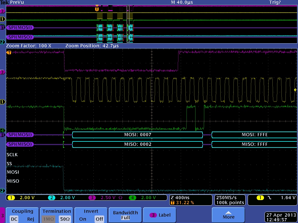
 

Next, I figured that what I would like to try is the low inactive without delay mode (2,0,0 CLKSTP, CLKXP, CLKRP).  However, when I set the ports to this mode, I see the strange behavior where the 16th clock pulse is held for some extra time, and in the last word, only 15 clock pulses are issued.  The result is 3 received words that are mangled and an incomplete 4th word.  See the capture entitled “no-delay-mode-missing-bit.jpg”.  This does not seem like it is working properly. If it was working, I would imagine this is the mode that I would like to use if the delay mode doesn't work. 


I have tried the other 2 modes mentioned in the manual, but neither of them work any better.  The “high inactive state without delay” (2,1,0) has the similar missing bit problem, whereas the “low inactive state with delay” (3,0,1) never seems to pass data to the McBSP ports at all!

 I am also attaching a third capture that shows a complete 4 word transmission from the 2 ports where the A port data is received properly, and the B port data running with the same configuration (3,1,1), clock and chip select but is shifted left by 1 bit.  This capture is called “delay-mode-2-ports.jpg”.  It seems to me that if it works for port A, it ought to work for port B as well.  I cannot understand how it is broken for 1 port but works for the other.  The data that the McBSP reports on port A for the following signal is correctly reported as 0x0007,0xFFFE,0xFFFF,0xFFFF.  However, the data that is recieved by port B during the same time is incorrectly reported as: 0x0005,0xFFFF,0xFFFD,0xFFFC
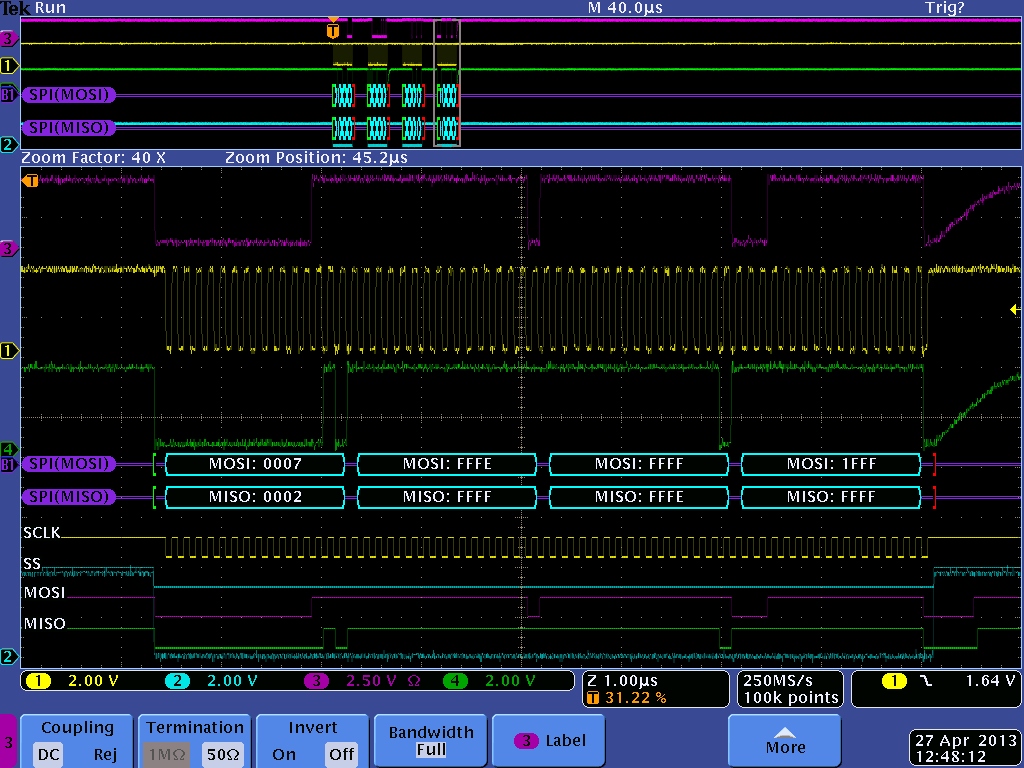
                                                                                                                                                                                      

Last but not least is a capture that illustrates this problem very plainly and easily.  This is a capture of the first full 16 bit word transmitted from the ADC to the DSP.  The port is configured to receive on the falling edge as usual.  The scope picks this up as a 1, but the McBSP reports it as a 3.  If you go through and count the falling edges in this picture, there is no way this could be construed as a 3.  It is only a 3 if you use 17 clock pulses for a word counting the falling edges, or if you skip the first clock altogether.  The only other possibility is that even though the port is configured to receive on the falling edge, it is actually receiving on the rising edge.  The name of this capture is “how-is-this-a-3.jpg”


I am attaching all of these scope captures for your review as well as my configuration for the DSP McBSP ports – A is a master, B is a slave.  If there is any other information you would like, please just let me know and I will be happy to assist.

 2642.mcbsp_config.cpp

As I said, I am sort of blocked on this because the received data is corrupted so I cannot move past this until I figure out how to correct it.  Any help, suggestions, or fixes would be most appreciated!

 Thanks!

 -Jeff

  • Hi!

    I'd like to do some remarks about your problem. May be it could help you.

    1 For either ADC the least significant bit is not very stable. This problem have a origin from the phisic principle of ADC's operation. For forming the least significant bit the comparator works at the sensibility limit. So, for example, the codes 0xFFFF, 0xFFFE, 0xFFFD and 0xFFFC is the same code with an accuracy up to a quantification noise. The least significant bit  should not be considered. Furthermore sometimes the quantification error can take place at the second bit also (for example, your results are 0x0007 and 0x0005). This is a normal phenomenon.

    2 I would advise you to change the algorithm of a data reception. You do simultaniously the execution of a ADC's converting , but the data reading should do sequentially from each ADC.

    Regards,

    Igor

  • Hi Igor,

    First off, thanks for your quick reply - I really appreciate it!  

    I fear that I have not explained the problem clear enough however. The problem is not one of least significant bits being off.  True in the case where you are just reading all F's, it would not matter at all if the LSB was a garbage bit.  No, my problem is the fact that ALL of the bits are shifted left by one, and in so doing the MOST significant bit is lost!  Perhaps if I used numbers other than all F's to illustrate it would have been clearer - I just grabbed what was on my scope at the time.  So consider a non-trivial example.  If the ADC gave back the number 0x95D7, what the McBSP would read would be 0x2BAE!  If it simply read out 0x95D6, I would agree with you and it would be no big deal.  However, losing the MSB and shifting all other bits has a drastic effect!  This is the problem I am really asking about - I hope this clears that up.

    As for your suggestion to read the values serially, I have tried this approach but unfortunately it is not possible because of timing.  I need to get the values off the ADC as fast as I possibly can because the next conversion needs to start before the amount of time it would take to either read them off of 2 ports in a serial manner, or even reading all of the values off port A and just use the 1 port!  I have also tried this as well.

    In fact, I am not sure this would even be possible in the first place.  The ADC only has 1 clock line and chip select, so it seems to me that the ADC is designed to clear its transmit buffers in a simultaneous manner.  There is not a different clock line assigned to each port on the ADC, so I believe that the data comes out of the B port at the same time as the A port no matter what. 

    Hopefully this clarifies my question somewhat.  I do appreciate your advice however!

    Thanks!

    -Jeff

  • Hi!

    0x95D7 : 1001010111010111

    0x2BAE :        10101110101110

    So you receive correctly first (7),  second (D) & third (5) tetrads. But there is one gash bit "0" and most significant tetrad (9) is received incompletely. Thusly, if your ADC transmits a most significant tetrad first at the bit sequence,  you begin receiving data too late (you lose 3 firsts bits). This is the problem of the start of ISR and a sinchronization. There is some delay. The begin of generation of clock and the begin of receiving should coincide. May be I write banalities, but I would like to begin with oscillograms and with the found of a strange delay.

    Regards,

    Igor 

  • Hi Igor, 

    Thanks for the suggestion.  However, there are no ISRs in this system - this is driven exclusively by DMA.  Moreover, there is only one clock signal and chip select that is in use between both McBSP ports as well as the ADC.  So they all have the same timing exactly and are running off the same signals.  Therefore, if it works for port A, I cannot understand how the timing could be different for port B.  They >should< be perfectly synchronized.

    The actual reception of the data is triggered by the McBSP RRDY flag indicating that the buffer has a word to receive.  When the word is in the buffer, the DMA will do the transfer.  The clock that puts the word in the buffer is the same clock that is putting the other word in the other port's receive buffer.  Weird.

  • Hi!

    I acknowledge this problem is not trivial. Notwithstanding I would prefer the use of one-channel data transfer mode for ADS8548 (refer datasheet):

    The output SDO_A is always active and exclusively used if only one serial data port is used in the application.
    The data are available in the following order: CH_A0, CH_A1, CH_B0, CH_B1, CH_C0, CH_C1, CH_D0, and
    CH_D1. (Fig. 39)

    The transfer time will be increased in all double  beside tow-channel data transfer mode.

    You write: The DMA then provides clock and chip select to the ADC. What signal is formed earlier on? The order should be following: Conversion, Chip select, Clock.

    Regards,

    Igor

  • Hi Jeff -


    I just saw this post from a couple of months ago and thought that I would update the response, in case someone is looking for a solution to this in the future. 

    TI has reported a similar problem except with a different ADC and the TI engineer's response (http://e2e.ti.com/support/microcontrollers/c2000/f/171/t/100545.aspx) is that in SPI slave mode, there is a documented limitation of the McBSP port implementation:  it can run only a maximum of LSPCLK/16, or in the case of the 28346 300MHz chip, it can run at a maximum of LSPCLK=150MHz/16=9.375MHz.  The master mode maximum rate, in comparison, is LSPCLK/4=37.5MHz.

    The other engineer experiencing a similar problem was also having the first bit out of the ADC thrown away by the McBSP slave port.  Note that TI does not document this issue in the reference manual for the McBSP ports which is usually considered the more detailed manual, but only in the data sheet of the 28346 chip.  There, TI has added this limitation is very large print to draw attention to it.  It appears that the McBSP port in slave mode needs to resynchronize the external SPI slave clock to its internal clock at the beginning of every SPI transfer (i.e., immediately after the transmit frame signal usually called \SPISTE goes low).  Apparently (and I am guessing here as they really don't say), they have a state machine to perform this resynchronization and it requires not more than 16 LSPCLK periods to complete the resynchronization.  During this time, it ignores any external clock edges that arrive before it is ready to receive them.  This is what causes the most significant bit to be dropped.  I have tried many other settings to attempt to get around this problem, but it only results in possibly dropping one more of the first bits transferred.  This also probably means that the rising edge of the framing signal (\SPISTE) cuts off the transfer before the McBSP thinks that it is finished since the McBSP port threw away the first clock while deciding what to do about it.  I don't think that it has any status flags to indicate an incomplete transfer.  It appears to simply stop the shift register on the rising edge of the external \SPISTE and give you the partial results.