Other Parts Discussed in Thread: TMS320F28335
Dear All,
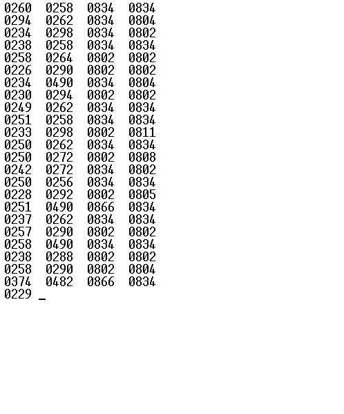
I am presently working with TMS320F28335. I have suddenly got some problem with the digital values. I am getting the digital values on serial port (as shown in the code below). I have implemented the low-pass filter for reducing the garbage values. Initially it was fine and I have seen the difference between with and without filter. But now both the values are same. I don't know why. Can anyone help me. I need to correct it urgently. Please help me. I am not understanding what's the problem.
Thanks a lot!
Here's the code below:
// TI File $Revision: /main/11 $
// Checkin $Date: April 21, 2008 15:41:01 $
//###########################################################################
//
// FILE: Example_2833xAdc.c
//
// TITLE: DSP2833x ADC Example Program.
//
// ASSUMPTIONS:
//
// This program requires the DSP2833x header files.
//
// Make sure the CPU clock speed is properly defined in
// DSP2833x_Examples.h before compiling this example.
//
// Connect signals to be converted to A2 and A3.
//
// As supplied, this project is configured for "boot to SARAM"
// operation. The 2833x Boot Mode table is shown below.
// For information on configuring the boot mode of an eZdsp,
// please refer to the documentation included with the eZdsp,
//
// $Boot_Table:
//
// GPIO87 GPIO86 GPIO85 GPIO84
// XA15 XA14 XA13 XA12
// PU PU PU PU
// ==========================================
// 1 1 1 1 Jump to Flash
// 1 1 1 0 SCI-A boot
// 1 1 0 1 SPI-A boot
// 1 1 0 0 I2C-A boot
// 1 0 1 1 eCAN-A boot
// 1 0 1 0 McBSP-A boot
// 1 0 0 1 Jump to XINTF x16
// 1 0 0 0 Jump to XINTF x32
// 0 1 1 1 Jump to OTP
// 0 1 1 0 Parallel GPIO I/O boot
// 0 1 0 1 Parallel XINTF boot
// 0 1 0 0 Jump to SARAM <- "boot to SARAM"
// 0 0 1 1 Branch to check boot mode
// 0 0 1 0 Boot to flash, bypass ADC cal
// 0 0 0 1 Boot to SARAM, bypass ADC cal
// 0 0 0 0 Boot to SCI-A, bypass ADC cal
// Boot_Table_End$
//
// DESCRIPTION:
//
// This example sets up the PLL in x10/2 mode.
//
// For 150 MHz devices (default)
// divides SYSCLKOUT by six to reach a 25.0Mhz HSPCLK
// (assuming a 30Mhz XCLKIN).
//
// For 100 MHz devices:
// divides SYSCLKOUT by four to reach a 25.0Mhz HSPCLK
// (assuming a 20Mhz XCLKIN).
//
// Interrupts are enabled and the ePWM1 is setup to generate a periodic
// ADC SOC on SEQ1. Two channels are converted, ADCINA3 and ADCINA2.
//
// Watch Variables:
//
// Voltage1[10] Last 10 ADCRESULT0 values
// Voltage2[10] Last 10 ADCRESULT1 values
// ConversionCount Current result number 0-9
// LoopCount Idle loop counter
//
//
//###########################################################################
//
// Original Author: D.F.
//
// $TI Release: DSP2833x/DSP2823x C/C++ Header Files V1.31 $
// $Release Date: August 4, 2009 $
//###########################################################################
#include "DSP28x_Project.h" // Device Headerfile and Examples Include File
#include <stdio.h>
// Global variables used in this example:
#define SZ_VOL 32
Uint16 LoopCount = 0;
Uint16 Voltage1[SZ_VOL];
Uint16 Voltage2[SZ_VOL];
Uint16 Voltage3[SZ_VOL];
Uint16 Voltage4[SZ_VOL];
Uint16 filteredVoltage1 = 0;
Uint16 filteredVoltage2 = 0;
Uint16 filteredVoltage3 = 0;
Uint16 filteredVoltage4 = 0;
Uint16 VoltageOut1 = 0;
Uint16 VoltageOut2 = 0;
Uint16 VoltageOut3 = 0;
Uint16 VoltageOut4 = 0;
#define SZ_MSG 20
#define MAX_SZ_MSG 30
Uint16 ReceivedChar;
Uint16 flgSend = 0;
char msg[SZ_MSG] = "\r\nStart.\0";
char total_msg[MAX_SZ_MSG] = "";
interrupt void adc_isr(void);
Uint16 low_pass_lim(Uint16 new, Uint16 old, float alpha);
void scia_fifo_init();
void scia_init();
void scia_xmit(int a);
void scia_msg(char * msg);
void d2asc(Uint16 in, char *asc);
void nullify(char * msg);
main()
{
// Step 1. Initialize System Control:
// PLL, WatchDog, enable Peripheral Clocks
// This example function is found in the DSP2833x_SysCtrl.c file.
InitSysCtrl();
EALLOW;
#if (CPU_FRQ_150MHZ) // Default - 150 MHz SYSCLKOUT
#define ADC_MODCLK 0x3 // HSPCLK = SYSCLKOUT/2*ADC_MODCLK2 = 150/(2*3) = 25.0 MHz
#endif
#if (CPU_FRQ_100MHZ)
#define ADC_MODCLK 0x2 // HSPCLK = SYSCLKOUT/2*ADC_MODCLK2 = 100/(2*2) = 25.0 MHz
#endif
EDIS;
// Step 2. Initialize GPIO:
// This example function is found in the DSP2833x_Gpio.c file and
// illustrates how to set the GPIO to it's default state.
//InitGpio(); // Skipped for this example
InitSciaGpio();
// Step 3. Clear all interrupts and initialize PIE vector table:
// Disable CPU interrupts
DINT;
// Initialize the PIE control registers to their default state.
// The default state is all PIE interrupts disabled and flags
// are cleared.
// This function is found in the DSP2833x_PieCtrl.c file.
InitPieCtrl();
// Disable CPU interrupts and clear all CPU interrupt flags:
IER = 0x0000;
IFR = 0x0000;
// Initialize the PIE vector table with pointers to the shell Interrupt
// Service Routines (ISR).
// This will populate the entire table, even if the interrupt
// is not used in this example. This is useful for debug purposes.
// The shell ISR routines are found in DSP2833x_DefaultIsr.c.
// This function is found in DSP2833x_PieVect.c.
InitPieVectTable();
// Interrupts that are used in this example are re-mapped to
// ISR functions found within this file.
EALLOW; // This is needed to write to EALLOW protected register
PieVectTable.ADCINT = &adc_isr;
EDIS; // This is needed to disable write to EALLOW protected registers
// Step 4. Initialize all the Device Peripherals:
// This function is found in DSP2833x_InitPeripherals.c
//InitPeripherals(); // Not required for this example
InitAdc(); // For this example, init the ADC
scia_fifo_init(); // Initialize the SCI FIFO
scia_init(); // Initalize SCI for echoback
ADC_cal();
// Step 5. User specific code, enable interrupts:
// Enable ADCINT in PIE
PieCtrlRegs.PIEIER1.bit.INTx6 = 1;
IER |= M_INT1; // Enable CPU Interrupt 1
EINT; // Enable Global interrupt INTM
ERTM; // Enable Global realtime interrupt DBGM
LoopCount = 0;
// Configure ADC
AdcRegs.ADCTRL3.bit.SMODE_SEL = 0x1;
AdcRegs.ADCMAXCONV.all = 0x0003; // Setup 2 conv's on SEQ1
AdcRegs.ADCCHSELSEQ1.bit.CONV00 = 0x4; // Setup ADCINA3 as 1st SEQ1 conv.
AdcRegs.ADCCHSELSEQ1.bit.CONV01 = 0x3; // Setup ADCINA2 as 2nd SEQ1 conv.
AdcRegs.ADCCHSELSEQ1.bit.CONV02 = 0x2; // Setup ADCINA1 as 3rd SEQ1 conv.
AdcRegs.ADCCHSELSEQ1.bit.CONV03 = 0x1; // Setup ADCINA0 as 4th SEQ1 conv.
AdcRegs.ADCTRL2.bit.EPWM_SOCA_SEQ1 = 1; // Enable SOCA from ePWM to start SEQ1
AdcRegs.ADCTRL2.bit.INT_ENA_SEQ1 = 1; // Enable SEQ1 interrupt (every EOS)
//AdcRegs.ADCTRL1.all=0x0710;
// Assumes ePWM1 clock is already enabled in InitSysCtrl();
EPwm1Regs.ETSEL.bit.SOCAEN = 1; // Enable SOC on A group
EPwm1Regs.ETSEL.bit.SOCASEL = 4; // Select SOC from from CPMA on upcount
EPwm1Regs.ETPS.bit.SOCAPRD = 1; // Generate pulse on 1st event
EPwm1Regs.CMPA.half.CMPA = 0x0080; // Set compare A value
EPwm1Regs.TBPRD = 0xFFFF; // Set period for ePWM1
//EPwm1Regs.TBPRD = 600;
EPwm1Regs.TBCTL.bit.CTRMODE = 0; // count up and start
scia_msg(msg);
// Wait for ADC interrupt
for(;;)
{
if (flgSend == 0){
scia_msg("\r");
d2asc(VoltageOut1, msg);
strcat(total_msg,msg);
d2asc(VoltageOut2, msg);
strcat(total_msg,msg);
//scia_msg("hello world");
d2asc(VoltageOut3, msg);
strcat(total_msg,msg);
d2asc(VoltageOut4, msg);
strcat(total_msg,msg);
scia_msg(total_msg);
//scia_msg("\n");
nullify(total_msg);
//scia_msg("\n");
flgSend = 1;
scia_msg("\n");
}
LoopCount++;
}
}
interrupt void adc_isr(void)
{
static int i = 0;
Voltage1[i] = AdcRegs.ADCRESULT0>>4;
Voltage2[i] = AdcRegs.ADCRESULT1>>4;
Voltage3[i] = AdcRegs.ADCRESULT2>>4;
Voltage4[i] = AdcRegs.ADCRESULT3>>4;
//Voltage1[i] = AdcRegs.ADCRESULT1>>4;
//Voltage2[i] = AdcRegs.ADCRESULT5>>4;
//Voltage3[i] = AdcRegs.ADCRESULT7>>4;
//Voltage4[i] = AdcRegs.ADCRESULT3>>4;
filteredVoltage1= low_pass_lim(Voltage1[i], filteredVoltage1, 0.15);
filteredVoltage2= low_pass_lim(Voltage2[i], filteredVoltage2, 0.15);
filteredVoltage3= low_pass_lim(Voltage3[i], filteredVoltage3, 0.15);
filteredVoltage4= low_pass_lim(Voltage4[i], filteredVoltage4, 0.15);
if (flgSend != 0){
//VoltageOut1 = filteredVoltage1;
//VoltageOut2 = filteredVoltage2;
//VoltageOut3 = filteredVoltage3;
//VoltageOut4 = filteredVoltage4;
VoltageOut1 = Voltage1[i];
VoltageOut2 = Voltage2[i];
VoltageOut3 = Voltage3[i];
VoltageOut4 = Voltage4[i];
flgSend = 0;
}
i++;
if(i>=SZ_VOL) i = 0;
// Reinitialize for next ADC sequence
AdcRegs.ADCTRL2.bit.RST_SEQ1 = 1; // Reset SEQ1
AdcRegs.ADCST.bit.INT_SEQ1_CLR = 1; // Clear INT SEQ1 bit
PieCtrlRegs.PIEACK.all = PIEACK_GROUP1; // Acknowledge interrupt to PIE
return;
}
Uint16 low_pass_lim(Uint16 new, Uint16 old, float alpha)
{
float tmp32_1 = 0.0;
float tmp32_2 = 0.0;
float tmp32_3 = 0.0;
tmp32_1 = (float)(new);
tmp32_2 = (float)(old);
tmp32_3 = alpha * tmp32_1 + (1.0 - alpha) * tmp32_2;
return (Uint16)(tmp32_3);
}
void scia_fifo_init()
{
SciaRegs.SCIFFTX.all=0xE040;
SciaRegs.SCIFFRX.all=0x204f;
SciaRegs.SCIFFCT.all=0x0;
}
// Test 1,SCIA DLB, 8-bit word, baud rate 0x000F, default, 1 STOP bit, no parity
void scia_init()
{
// Note: Clocks were turned on to the SCIA peripheral
// in the InitSysCtrl() function
SciaRegs.SCICCR.all =0x0007; // 1 stop bit, No loopback
// No parity,8 char bits,
// async mode, idle-line protocol
SciaRegs.SCICTL1.all =0x0003; // enable TX, RX, internal SCICLK,
// Disable RX ERR, SLEEP, TXWAKE
SciaRegs.SCICTL2.all =0x0003;
SciaRegs.SCICTL2.bit.TXINTENA =1;
SciaRegs.SCICTL2.bit.RXBKINTENA =1;
#if (CPU_FRQ_150MHZ)
SciaRegs.SCIHBAUD =0x0001; // 9600 baud @LSPCLK = 37.5MHz.
SciaRegs.SCILBAUD =0x00E7;
//SciaRegs.SCIHBAUD =0x0000; // 115,200 baud @LSPCLK = 37.5MHz.
//SciaRegs.SCILBAUD =0x0028;
#endif
#if (CPU_FRQ_100MHZ)
SciaRegs.SCIHBAUD =0x0001; // 9600 baud @LSPCLK = 20MHz.
SciaRegs.SCILBAUD =0x0044;
#endif
SciaRegs.SCICTL1.all =0x0023; // Relinquish SCI from Reset
}
void scia_xmit(int a)
{
while (SciaRegs.SCIFFTX.bit.TXFFST != 0) {}
SciaRegs.SCITXBUF=a;
}
void scia_msg(char *in)
{
int i;
i = 0;
while(in[i] != '\0')
{
scia_xmit(in[i]);
i++;
}
}
void d2asc(Uint16 in, char *asc)
{
float tmp1, tmp2;
char out, out_tmp;
asc[0] = ' ';
asc[1] = ' ';
tmp1 = (float)(in);
tmp2 = (float)(tmp1) * 0.001;
out_tmp = (char)(tmp2);
out = out_tmp + 0x30;
asc[2] = out;
tmp1 = tmp1 - (float)(out_tmp) * 1000.0;
tmp2 = (float)(tmp1) * 0.01;
out_tmp = (char)(tmp2);
out = out_tmp + 0x30;
asc[3] = out;
tmp1 = tmp1 - (float)(out_tmp) * 100.0;
tmp2 = (float)(tmp1) * 0.1;
out_tmp = (char)(tmp2);
out = out_tmp + 0x30;
asc[4] = out;
tmp1 = tmp1 - (float)(out_tmp) * 10.0;
tmp2 = (float)(tmp1) * 1.0;
out_tmp = (char)(tmp2);
out = out_tmp + 0x30;
asc[5] = out;
asc[6] = '\0';
}
void nullify( char * msg ) {
int i;
for ( i = 0; i < MAX_SZ_MSG; i++)
msg[i] = '\0';
}