This thread has been locked.

If you have a related question, please click the "Ask a related question" button in the top right corner. The newly created question will be automatically linked to this question.

How do i configure ADC to measure two signals simultaneously?

Hi everyone, How do i configure ADC to measure two signals simultaneously? , i'm working with a F28027 Piccolo microcontroler, sorry if my question is outrageous, regards..

  • Mileva,

    It depends on how simultaneous you really want the two conversions to be. If two SOCs are setup to start based on the same trigger (say an ePWM), then when that trigger is received, one will convert, then the other.  The time difference will be about 216ns, which may be close enough depending on your application.

    If you want them to occur at exactly the same time, you would set the bit for your SOC of interest in the ADCSAMPLEMODE register.  When the SOC is triggered, two samples are captured simultaneously, and then the converter processes the two voltages sequentially.  

  • Hi Devin, then i set  AdcRegs.ADCSAMPLEMODE.bit.SIMULEN0 = 1;  and how do i configure to ADCSOCxCTL to measure for example the signal of PWM2?, in the case of i'll have to feedback EPWM-2A with the ADC-A1..

  • Mileva,

    If you have enabled simultaneous mode for SOC0, you still configure SOC0 as normal. The only difference is, you will convert two signal with one trigger (you will want something other than EPWM-2A to convert also).

    You would set CHSEL based on the channels you want to sample (e.g. CHSEL = 0 will select A0/B0, CHSEL = 3 will select A3/B3).  

    You select ACQPS such that the acquisition window is large enough for the signal on A0/B0 with the highest output impedance.

    You select TRIGSEL based on whatever you want to trigger the conversion of both signals.  

    Once the conversions are complete, the results for A channel will be in ADCRESULT0 and the results for B channel will be in ADCRESULT1

    Please refer to the ADC user guide for more details: spruge5f

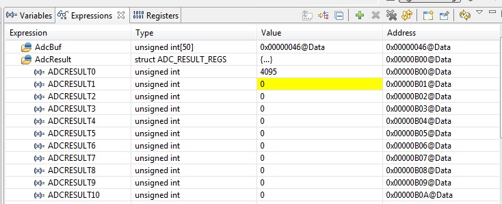
  • Devin, i did that, but the signal sample in the ADCRESULT1 is not right, and the signal in the ADCRESULT0 is more or less ok,,,, i'll paste my "Adc.c" code bellow:

    void InitAdc(void)
    {
    asm(" EALLOW"); // Enable EALLOW protected register access

    //--- Reset the ADC module
    // Note: The ADC is already reset after a DSP reset, but this example is just showing
    // good coding practice to reset the peripheral before configuring it as you never
    // know why the DSP has started the code over again from the beginning).
    AdcRegs.ADCCTL1.bit.RESET = 1; // Reset the ADC

    // Must wait 2 ADCCLK periods for the reset to take effect.
    // Note that ADCCLK = SYSCLKOUT for F2802x/F2803x devices.
    asm(" NOP");
    asm(" NOP");

    //--- Power-up and configure the ADC
    AdcRegs.ADCCTL1.all = 0x00E4; // Power-up reference and main ADC

    DelayUs(1000); // Wait 1 ms after power-up before using the ADC

    //--- SOC0 configuration
    //AdcRegs.ADCSAMPLEMODE.bit.SIMULEN0 = 0; // SOC0 in single sample mode (vs. simultaneous mode)

    //AdcRegs.ADCSOC0CTL.bit.TRIGSEL = 9; //// Trigger using ePWM3-ADCSOCA
    //AdcRegs.ADCSOC0CTL.bit.CHSEL = 0; // Convert channel ADCINA0 (ch0) with SIMULEN=1 (CHSEL=0 ==> ADCINA0 y ADCINB0)

    AdcRegs.ADCSAMPLEMODE.bit.SIMULEN0 = 1; // 
    DelayUs(1000);

    AdcRegs.ADCCTL1.bit.INTPULSEPOS = 1; //0; //1;
    ///// SOCs
    AdcRegs.ADCSOC0CTL.bit.TRIGSEL = 9; //(ADC3)
    AdcRegs.ADCSOC0CTL.bit.CHSEL = 0; //2; // pagina 15/44 Piccolo ADC.pdf
    DelayUs(1000);

    AdcRegs.ADCSOC0CTL.bit.ACQPS = 25; //9; //6;// 25;//6; // Acquisition window set to (6+1)=7 cycles

    AdcRegs.ADCINTSOCSEL1.bit.SOC0 = 0; // 1; // No ADCINT triggers SOC0. TRIGSEL field determines trigger.
    // DelayUs(1000);
    AdcRegs.SOCPRICTL.bit.SOCPRIORITY = 0; // All SOCs handled in round-robin mode
    //////////// SOCs

    //--- ADCINT0 configuration
    AdcRegs.INTSEL1N2.bit.INT1CONT = 0; //0; // ADCINT0 pulses generated only when ADCINT0 flag is clear
    AdcRegs.INTSEL1N2.bit.INT1E = 1; // Enable ADCINT0
    AdcRegs.INTSEL1N2.bit.INT1SEL = 0; // EOC0 triggers ADCINT0
    // AdcRegs.INTSEL1N2.bit.INT1SEL = 1; // EOC1 triggers ADCINT0
    //-- fin ADCINT0 CONFIGuration

    PieCtrlRegs.PIEIER1.bit.INTx1 = 1; // Enable ADCINT0 in PIE group 1

    IER |= 0x0001; // Enable INT1 in IER to enable PIE group


    //--- Finish up
    AdcRegs.ADCCTL1.bit.ADCENABLE = 1; // Enable the ADC
    asm(" EDIS"); // Disable EALLOW protected register access

    } // end InitAdc()


    ////////////////////////////////////////////////////////////////////////////////////////////////////////////////////////////////////////////////////////////

    Signals respectively are bellow AdcBuf, ADCRESULT0 and ADCRESULT1:


    AdcBuf(epwm1 and epwm2 are not out of phase) <==(IMPORTANT)

    There is no phase shift between the signals.

    ADCRESULT0:


    ADCRESULT1:

    I really apreciete any suggestions, explanation or warning to configure ADc to measure two signals simultaneously, regards..

  • Some thoughts:

    You reset the ADC:

    AdcRegs.ADCCTL1.bit.RESET = 1;

    This will clear the device trim.  Do you call the device calibration function sometime after this?  If not, your results will be subject to large errors.

    Have you looked at the device errata?  I think you may need to make some changes to account for the first sample issue.

    Either way, it doesn't look like you are getting any signal on ADCB0.  The amplitude of the signal is only 8 LSBs, which is probably just noise.  You will probably want to make sure the signal is actually making it to the ADC B0 pin using an oscilloscope.