This thread has been locked.

If you have a related question, please click the "Ask a related question" button in the top right corner. The newly created question will be automatically linked to this question.

How to port HVMotorCtrl+PfcKit_v2.0 HVACI code from F28035 to F28069?

Other Parts Discussed in Thread: CONTROLSUITE, DRV8301

Hi,

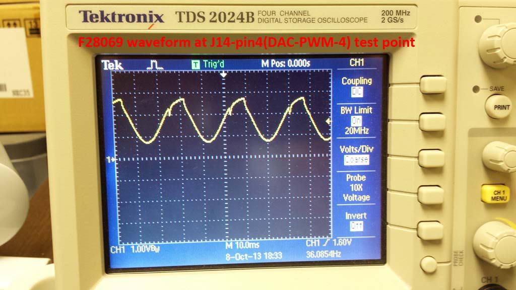
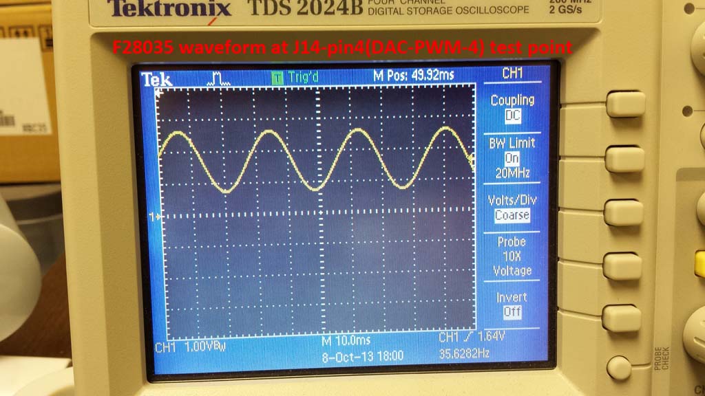
I am working on an ACIM VFD project with TMDSHVMTRPFCKIT + F28035 controlCARD now, however, my customer wants to use F28069 instead of F28035. Can anyone give me some suggestions on porting following HVMotorCtrl+PfcKit_v2.0 HVACI code from F28035 to F28069?

C:\ti\controlSUITE\development_kits\HVMotorCtrl+PfcKit_v2.0\HVACI_Sensorless

C:\ti\controlSUITE\development_kits\HVMotorCtrl+PfcKit_v2.0\HVACI_Scalar

C:\ti\controlSUITE\development_kits\HVMotorCtrl+PfcKit_v2.0\HVACI_Sensored


Thanks a lot.


Bill

  • Biao,

    You can move this to F28069, first you will need to point the project to the f2806x device support files and compile the code. Do not use the floating point code make sure you select the fixed point rts library.  

    (This will make the code running with fixed point on F2806x)

    then you can look at the code for F2833x for AC induction control, there are few things that change between fixed point and floating point processor i.e. ADC reading updating the PWM etc, the rest should be taken care of the float to fixed switch in the IQ math library (A good example of this is the ACI F2833x example which supports both F28035 config and F2833x),

    You must make sure MATH_TYPE is defined as 1 before you include the IQ math library that is done in the settings.h file. 

    #define MATH_TYPE 1 

     Enable floating point in the build settings, also you will have to relink to the IQmath_fpu.lib instead of just IQmath.lib and also make sure the rts lib is floating point version

  • Manish,

    I will try it. Thanks for your help.

    Bill

  • Biao,

    in controlSUITE see the DRV8301 kit. These projects are dual built for F28035 and F28069, both using fixed point and IQMath. This should teach you how to move any project from one device to another.  BUT, if you want to start using floating point in the project it does become more complex.  But just moving to fixed is a good start.


  • Hi Chris,

    Yes. I have found the code for both F28035 and F28069 in the following folder, and I have already made my kit work with F28069 controlCard now.

    C:\ti\controlSUITE\development_kits\DRV8312-C2-KIT_v128\PM_Sensorless

    Thanks for your help.

    Biao

  • Chris,

    I have done the code porting from F28035 to F28069 based on HVMotorCtrl+PfcKit_v2.0 HVACI\HVACI_Sensorless code, however, I found the F28069 output waveform at HVMotorCtrl+PfcKit_v2.0 J14-pin4 (DAC-PWM-4) test point is not as good as the output of F28035 when I run LEVEL1 built code. I am using fixed point for F28069 now.

    Please see attached waveform photos. Could you please help me figure out this issue?

    Thanks a lot.

    Biao

    Figure 1. F28069 output waveform at J14-Pin4 (DAC-PWM-4) test point

    Figure 2. F28035 output waveform at J14-Pin4 (DAC-PWM-4) test point

  • certainly not a waveform you want to see!

    I've passed this along to someone else, hopefully they can help. my first instinct is to look at the set-up for the clocking and ePWM module.

  • Thanks Chris.

    Biao

  • Biao,

    what compiler are you using?  Right click on the project and look at the properties.

    Should be between 6.1.5 and 6.2.1


  • Chris,

    The compiler I am using is v6.1.0. Thanks.

    Biao

  • darn, I was hoping this was tied to the issues we're seeing with optimization settings on compiler 6.2.x


  • Chris,

    Any progress on the waveform issue which I posted about 2 weeks ago? I will demo my HV ACIM VFD prototype to my customer early next month. Could you please help me fix it at your early convenient time? I really need your help.

    Thanks a lot.

    Biao

  • Sorry, no.

    I would check the initialization of the ePWM and ADC modules.

    You can also monitor the outputs of the SVGEN or CLARKE modules, but I think that will just confirm the glitch in the output and not solve the root cause.

    Are you only using fixed point code on the F2806x?  If using floating point there could be a mistake in how that variable is being used.  Just thinking out loud....


  • Chris,

    I am using fixed point. Thanks.

    Biao

  • Biao,

    Assuming that your code is similar to the HVACI_Sensorless code, can you send across your "HVACI_Sensorless-DevInit_****.c" file? 

    If so, I'll take a look at it to see if I can spot anything wrong in it.


    Thank you,
    Brett

  • Biao,

    Can you verify other pins in that header. They should be clean sine waves. Can you post those waveforms as well.

    Also, It will help if you can review the code for LEVEL1. There is not much intelligence  in the code other than to use SVM to generate three phase duty cycles.

    rgds,

    ramesh

  • Hi Brett,

    Please see attached Devinit file.

    //============================================================================
    // FILE:	HVACI_Sensorless-DevInit_F2803x.c
    //============================================================================
    
    
    /***************************
    Note that the CLA is not used nor initialized in this project. Please download 
    the Peripheral Files and Example Projects collection (SPRC832) and look at the 
    cla_adc project for information on how to use and configure the CLA.
    ***************************/
    
    #include "PeripheralHeaderIncludes.h"
    
    // Functions that will be run from RAM need to be assigned to
    // a different section.  This section will then be mapped to a load and
    // run address using the linker cmd file.
    #pragma CODE_SECTION(InitFlash, "ramfuncs");
    #define Device_cal (void   (*)(void))0x3D7C80
    
    void DeviceInit(void);
    void PieCntlInit(void);
    void PieVectTableInit(void);
    void WDogDisable(void);
    void PLLset(Uint16);
    void ISR_ILLEGAL(void);
    
    //--------------------------------------------------------------------
    //  Configure Device for target Application Here
    //--------------------------------------------------------------------
    void DeviceInit(void)
    {
    	WDogDisable(); 	// Disable the watchdog initially
    	DINT;			// Global Disable all Interrupts
    	IER = 0x0000;	// Disable CPU interrupts
    	IFR = 0x0000;	// Clear all CPU interrupt flags
    
    
    // Switch to Internal Oscillator 1 and turn off all other clock
    // sources to minimize power consumption
    	EALLOW;
    	SysCtrlRegs.CLKCTL.bit.INTOSC1OFF = 0;
        SysCtrlRegs.CLKCTL.bit.OSCCLKSRCSEL=0;  // Clk Src = INTOSC1
    	SysCtrlRegs.CLKCTL.bit.XCLKINOFF=1;     // Turn off XCLKIN
    	SysCtrlRegs.CLKCTL.bit.XTALOSCOFF=1;    // Turn off XTALOSC
    	SysCtrlRegs.CLKCTL.bit.INTOSC2OFF=1;    // Turn off INTOSC2
        EDIS;
    
    
    // SYSTEM CLOCK speed based on internal oscillator = 10 MHz
    // 0xC =  60	MHz		(12)
    // 0xB =  55	MHz		(11)
    // 0xA =  50	MHz		(10)
    // 0x9 =  45	MHz		(9)
    // 0x8 =  40	MHz		(8)
    // 0x7 =  35	MHz		(7)
    // 0x6 =  30	MHz		(6)
    // 0x5 =  25	MHz		(5)
    // 0x4 =  20	MHz		(4)
    // 0x3 =  15	MHz		(3)
    // 0x2 =  10	MHz		(2)
    
    	PLLset(0xC);	// choose from options above
    
    // Initialise interrupt controller and Vector Table
    // to defaults for now. Application ISR mapping done later.
    	PieCntlInit();		
    	PieVectTableInit();
    
       EALLOW; // below registers are "protected", allow access.
    
    // LOW SPEED CLOCKS prescale register settings
       SysCtrlRegs.LOSPCP.all = 0x0002;		// Sysclk / 4 (15 MHz)
       SysCtrlRegs.XCLK.bit.XCLKOUTDIV=2;
          
          
    // ADC CALIBRATION 
    //---------------------------------------------------
    // The Device_cal function, which copies the ADC & oscillator calibration values
    // from TI reserved OTP into the appropriate trim registers, occurs automatically
    // in the Boot ROM. If the boot ROM code is bypassed during the debug process, the
    // following function MUST be called for the ADC and oscillators to function according
    // to specification.
    
    	SysCtrlRegs.PCLKCR0.bit.ADCENCLK = 1; // Enable ADC peripheral clock
    	(*Device_cal)();					  // Auto-calibrate from TI OTP
    	SysCtrlRegs.PCLKCR0.bit.ADCENCLK = 0; // Return ADC clock to original state     
    
          	
    // PERIPHERAL CLOCK ENABLES 
    //---------------------------------------------------
    // If you are not using a peripheral you may want to switch
    // the clock off to save power, i.e. set to =0 
    // 
    // Note: not all peripherals are available on all 280x derivates.
    // Refer to the datasheet for your particular device. 
    
       SysCtrlRegs.PCLKCR0.bit.ADCENCLK = 1;    // ADC
       //------------------------------------------------
       SysCtrlRegs.PCLKCR3.bit.COMP1ENCLK = 1;	// COMP1
       SysCtrlRegs.PCLKCR3.bit.COMP2ENCLK = 1;	// COMP2
       SysCtrlRegs.PCLKCR3.bit.COMP3ENCLK = 1;  // COMP3
       //------------------------------------------------
       SysCtrlRegs.PCLKCR1.bit.ECAP1ENCLK = 1;	//eCAP1
       //------------------------------------------------
       SysCtrlRegs.PCLKCR0.bit.ECANAENCLK=0;   // eCAN-A
       //------------------------------------------------
       SysCtrlRegs.PCLKCR1.bit.EQEP1ENCLK = 1;  // eQEP1
       //------------------------------------------------
       SysCtrlRegs.PCLKCR1.bit.EPWM1ENCLK = 1;  // ePWM1
       SysCtrlRegs.PCLKCR1.bit.EPWM2ENCLK = 1;  // ePWM2
       SysCtrlRegs.PCLKCR1.bit.EPWM3ENCLK = 1;  // ePWM3
       SysCtrlRegs.PCLKCR1.bit.EPWM4ENCLK = 1;  // ePWM4
       SysCtrlRegs.PCLKCR1.bit.EPWM5ENCLK = 1;	// ePWM5
       SysCtrlRegs.PCLKCR1.bit.EPWM6ENCLK = 1;	// ePWM6
       SysCtrlRegs.PCLKCR1.bit.EPWM7ENCLK = 1;	// ePWM7
       SysCtrlRegs.PCLKCR0.bit.HRPWMENCLK = 0;    // HRPWM
       //------------------------------------------------
       SysCtrlRegs.PCLKCR0.bit.I2CAENCLK = 0;   // I2C
       //------------------------------------------------
       SysCtrlRegs.PCLKCR0.bit.LINAENCLK = 0;   // LIN-A
       //------------------------------------------------
       SysCtrlRegs.PCLKCR3.bit.CLA1ENCLK = 0;   // CLA1
       //------------------------------------------------
       SysCtrlRegs.PCLKCR0.bit.SCIAENCLK = 1;  	// SCI-A
       //------------------------------------------------
       SysCtrlRegs.PCLKCR0.bit.SPIAENCLK = 0;	// SPI-A
       SysCtrlRegs.PCLKCR0.bit.SPIBENCLK = 0;   // SPI-B
       //------------------------------------------------
       SysCtrlRegs.PCLKCR0.bit.TBCLKSYNC = 1;   // Enable TBCLK
       //------------------------------------------------           


    //--------------------------------------------------------------------------------------
    // GPIO (GENERAL PURPOSE I/O) CONFIG
    //--------------------------------------------------------------------------------------
    //-----------------------
    // QUICK NOTES on USAGE:
    //-----------------------
    // If GpioCtrlRegs.GP?MUX?bit.GPIO?= 1, 2 or 3 (i.e. Non GPIO func), then leave
    //	rest of lines commented
    // If GpioCtrlRegs.GP?MUX?bit.GPIO?= 0 (i.e. GPIO func), then:
    //	1) uncomment GpioCtrlRegs.GP?DIR.bit.GPIO? = ? and choose pin to be IN or OUT
    //	2) If IN, can leave next to lines commented
    //	3) If OUT, uncomment line with ..GPACLEAR.. to force pin LOW or
    //			   uncomment line with ..GPASET.. to force pin HIGH or
    //--------------------------------------------------------------------------------------
    //--------------------------------------------------------------------------------------
    //  GPIO-00 - PIN FUNCTION = PWM1A
    	GpioCtrlRegs.GPAMUX1.bit.GPIO0 = 1;		// 0=GPIO,  1=EPWM1A,  2=Resv,  3=Resv
    //	GpioCtrlRegs.GPADIR.bit.GPIO0 = 1;		// 1=OUTput,  0=INput 
    //	GpioDataRegs.GPACLEAR.bit.GPIO0 = 1;	// uncomment if --> Set Low initially
    //	GpioDataRegs.GPASET.bit.GPIO0 = 1;		// uncomment if --> Set High initially
    //--------------------------------------------------------------------------------------
    //  GPIO-01 - PIN FUNCTION = PWM1B
    	GpioCtrlRegs.GPAMUX1.bit.GPIO1 = 1;		// 0=GPIO,  1=EPWM1B,  2=Resv,  3=COMP1OUT
    //	GpioCtrlRegs.GPADIR.bit.GPIO1 = 1;		// 1=OUTput,  0=INput 
    //	GpioDataRegs.GPACLEAR.bit.GPIO1 = 1;	// uncomment if --> Set Low initially
    //	GpioDataRegs.GPASET.bit.GPIO1 = 1;		// uncomment if --> Set High initially
    //--------------------------------------------------------------------------------------
    //  GPIO-02 - PIN FUNCTION = PWM2A
    	GpioCtrlRegs.GPAMUX1.bit.GPIO2 = 1;		// 0=GPIO,  1=EPWM2A,  2=Resv,  3=Resv
    //	GpioCtrlRegs.GPADIR.bit.GPIO2 = 0;		// 1=OUTput,  0=INput 
    //	GpioDataRegs.GPACLEAR.bit.GPIO2 = 1;	// uncomment if --> Set Low initially
    //	GpioDataRegs.GPASET.bit.GPIO2 = 1;		// uncomment if --> Set High initially
    //--------------------------------------------------------------------------------------
    //  GPIO-03 - PIN FUNCTION = PWM2B
    	GpioCtrlRegs.GPAMUX1.bit.GPIO3 = 1;		// 0=GPIO,  1=EPWM2B,  2=SPISOMI-A,  3=COMP2OUT
    //	GpioCtrlRegs.GPADIR.bit.GPIO3 = 0;		// 1=OUTput,  0=INput 
    //	GpioDataRegs.GPACLEAR.bit.GPIO3 = 1;	// uncomment if --> Set Low initially
    //	GpioDataRegs.GPASET.bit.GPIO3 = 1;		// uncomment if --> Set High initially
    //--------------------------------------------------------------------------------------
    //  GPIO-04 - PIN FUNCTION = PWM3A
    	GpioCtrlRegs.GPAMUX1.bit.GPIO4 = 1;		// 0=GPIO,  1=EPWM3A,  2=Resv,  3=Resv
    //	GpioCtrlRegs.GPADIR.bit.GPIO4 = 0;		// 1=OUTput,  0=INput 
    //	GpioDataRegs.GPACLEAR.bit.GPIO4 = 1;	// uncomment if --> Set Low initially
    //	GpioDataRegs.GPASET.bit.GPIO4 = 1;		// uncomment if --> Set High initially
    //--------------------------------------------------------------------------------------
    //  GPIO-05 - PIN FUNCTION = PWM3B
    	GpioCtrlRegs.GPAMUX1.bit.GPIO5 = 1;		// 0=GPIO,  1=EPWM3B,  2=SPISIMO-A,  3=ECAP1
    //	GpioCtrlRegs.GPADIR.bit.GPIO5 = 0;		// 1=OUTput,  0=INput 
    //	GpioDataRegs.GPACLEAR.bit.GPIO5 = 1;	// uncomment if --> Set Low initially
    //	GpioDataRegs.GPASET.bit.GPIO5 = 1;		// uncomment if --> Set High initially
    //--------------------------------------------------------------------------------------
    //  GPIO-06 - PIN FUNCTION = PWM4A
    	GpioCtrlRegs.GPAMUX1.bit.GPIO6 = 1;		// 0=GPIO,  1=EPWM4A,  2=SYNCI,  3=SYNCO
    //	GpioCtrlRegs.GPADIR.bit.GPIO6 = 0;		// 1=OUTput,  0=INput 
    //	GpioDataRegs.GPACLEAR.bit.GPIO6 = 1;	// uncomment if --> Set Low initially
    //	GpioDataRegs.GPASET.bit.GPIO6 = 1;		// uncomment if --> Set High initially
    //--------------------------------------------------------------------------------------
    //  GPIO-07 - PIN FUNCTION = PWM4B
    	GpioCtrlRegs.GPAMUX1.bit.GPIO7 = 1;		// 0=GPIO,  1=EPWM4B,  2=SCIRX-A,  3=Resv
    //	GpioCtrlRegs.GPADIR.bit.GPIO7 = 0;		// 1=OUTput,  0=INput 
    //	GpioDataRegs.GPACLEAR.bit.GPIO7 = 1;	// uncomment if --> Set Low initially
    //	GpioDataRegs.GPASET.bit.GPIO7 = 1;		// uncomment if --> Set High initially
    //--------------------------------------------------------------------------------------
    //  GPIO-08 - PIN FUNCTION = --Spare--
    	GpioCtrlRegs.GPAMUX1.bit.GPIO8 = 1;		// 0=GPIO,  1=EPWM5A,  2=Resv,  3=ADCSOC-A
    //	GpioCtrlRegs.GPADIR.bit.GPIO8 = 0;		// 1=OUTput,  0=INput 
    //	GpioDataRegs.GPACLEAR.bit.GPIO8 = 1;	// uncomment if --> Set Low initially
    //	GpioDataRegs.GPASET.bit.GPIO8 = 1;		// uncomment if --> Set High initially
    //--------------------------------------------------------------------------------------
    //  GPIO-09 - PIN FUNCTION = Clear Fault
    	GpioCtrlRegs.GPAMUX1.bit.GPIO9 = 0;		// 0=GPIO,  1=EPWM5B,  2=LINTX-A,  3=Resv
    	GpioCtrlRegs.GPADIR.bit.GPIO9 = 1;		// 1=OUTput,  0=INput 
    //	GpioDataRegs.GPACLEAR.bit.GPIO9 = 1;	// uncomment if --> Set Low initially
    	GpioDataRegs.GPASET.bit.GPIO9 = 1;		// uncomment if --> Set High initially
    //--------------------------------------------------------------------------------------
    //  GPIO-10 - PIN FUNCTION = PWM6A
    	GpioCtrlRegs.GPAMUX1.bit.GPIO10 = 1;	// 0=GPIO,  1=EPWM6A,  2=Resv,  3=ADCSOC-B
    //	GpioCtrlRegs.GPADIR.bit.GPIO10 = 0;		// 1=OUTput,  0=INput 
    //	GpioDataRegs.GPACLEAR.bit.GPIO10 = 1;	// uncomment if --> Set Low initially
    //	GpioDataRegs.GPASET.bit.GPIO10 = 1;		// uncomment if --> Set High initially
    //--------------------------------------------------------------------------------------
    //  GPIO-11 - PIN FUNCTION = PWM6B
    	GpioCtrlRegs.GPAMUX1.bit.GPIO11 = 1;	// 0=GPIO,  1=EPWM6B,  2=LINRX-A,  3=Resv
    //	GpioCtrlRegs.GPADIR.bit.GPIO11 = 0;		// 1=OUTput,  0=INput 
    //	GpioDataRegs.GPACLEAR.bit.GPIO11 = 1;	// uncomment if --> Set Low initially
    //	GpioDataRegs.GPASET.bit.GPIO11 = 1;		// uncomment if --> Set High initially
    //--------------------------------------------------------------------------------------
    //  GPIO-12 - PIN FUNCTION = TZ1
    	GpioCtrlRegs.GPAMUX1.bit.GPIO12 = 1;	// 0=GPIO,  1=TZ1,  2=SCITX-A,  3=SPISIMO-B
    //	GpioCtrlRegs.GPADIR.bit.GPIO12 = 0;		// 1=OUTput,  0=INput 
    //	GpioDataRegs.GPACLEAR.bit.GPIO12 = 1;	// uncomment if --> Set Low initially
    //	GpioDataRegs.GPASET.bit.GPIO12 = 1;		// uncomment if --> Set High initially
    //--------------------------------------------------------------------------------------
    //  GPIO-13 - PIN FUNCTION = --Spare--
    	GpioCtrlRegs.GPAMUX1.bit.GPIO13 = 0;	// 0=GPIO,  1=TZ2,  2=Resv,  3=SPISOMI-B
    	GpioCtrlRegs.GPADIR.bit.GPIO13 = 0;		// 1=OUTput,  0=INput 
    //	GpioDataRegs.GPACLEAR.bit.GPIO13 = 1;	// uncomment if --> Set Low initially
    //	GpioDataRegs.GPASET.bit.GPIO13 = 1;		// uncomment if --> Set High initially
    //--------------------------------------------------------------------------------------
    //  GPIO-14 - PIN FUNCTION = --Spare--
    	GpioCtrlRegs.GPAMUX1.bit.GPIO14 = 0;	// 0=GPIO,  1=TZ3,  2=LINTX-A,  3=SPICLK-B
    	GpioCtrlRegs.GPADIR.bit.GPIO14 = 0;		// 1=OUTput,  0=INput 
    //	GpioDataRegs.GPACLEAR.bit.GPIO14 = 1;	// uncomment if --> Set Low initially
    //	GpioDataRegs.GPASET.bit.GPIO14 = 1;		// uncomment if --> Set High initially
    //--------------------------------------------------------------------------------------
    //  GPIO-15 - PIN FUNCTION = OCP
    	GpioCtrlRegs.GPAMUX1.bit.GPIO15 = 0;	// 0=GPIO,  1=TZ1,  2=LINRX-A,  3=SPISTE-B
    	GpioCtrlRegs.GPADIR.bit.GPIO15 = 0;		// 1=OUTput,  0=INput 
    //	GpioDataRegs.GPACLEAR.bit.GPIO15 = 1;	// uncomment if --> Set Low initially
    //	GpioDataRegs.GPASET.bit.GPIO15 = 1;		// uncomment if --> Set High initially
    //--------------------------------------------------------------------------------------
    //--------------------------------------------------------------------------------------
    //  GPIO-16 - PIN FUNCTION = SPISIMO-A
    	GpioCtrlRegs.GPAMUX2.bit.GPIO16 = 1;	// 0=GPIO,  1=SPISIMO-A,  2=Resv,  3=TZ2
    //	GpioCtrlRegs.GPADIR.bit.GPIO16 = 0;		// 1=OUTput,  0=INput 
    //	GpioDataRegs.GPACLEAR.bit.GPIO16 = 1;	// uncomment if --> Set Low initially
    //	GpioDataRegs.GPASET.bit.GPIO16 = 1;		// uncomment if --> Set High initially
    //--------------------------------------------------------------------------------------
    //  GPIO-17 - PIN FUNCTION = SPISOMI-A
    	GpioCtrlRegs.GPAMUX2.bit.GPIO17 = 1;	// 0=GPIO,  1=SPISOMI-A,  2=Resv,  3=TZ3
    //	GpioCtrlRegs.GPADIR.bit.GPIO17 = 0;		// 1=OUTput,  0=INput 
    //	GpioDataRegs.GPACLEAR.bit.GPIO17 = 1;	// uncomment if --> Set Low initially
    //	GpioDataRegs.GPASET.bit.GPIO17 = 1;		// uncomment if --> Set High initially
    //--------------------------------------------------------------------------------------
    //  GPIO-18 - PIN FUNCTION = SPICLK-A
    	GpioCtrlRegs.GPAMUX2.bit.GPIO18 = 1;	// 0=GPIO,  1=SPICLK-A,  2=LINTX-A,  3=XCLKOUT
    //	GpioCtrlRegs.GPADIR.bit.GPIO18 = 1;		// 1=OUTput,  0=INput 
    //	GpioDataRegs.GPACLEAR.bit.GPIO18 = 1;	// uncomment if --> Set Low initially
    //	GpioDataRegs.GPASET.bit.GPIO18 = 1;		// uncomment if --> Set High initially
    //--------------------------------------------------------------------------------------
    //  GPIO-19 - PIN FUNCTION = SPISTE-A
    	GpioCtrlRegs.GPAMUX2.bit.GPIO19 = 1;	// 0=GPIO,  1=SPISTE-A,  2=LINRX-A,  3=ECAP1
    //	GpioCtrlRegs.GPADIR.bit.GPIO19 = 0;		// 1=OUTput,  0=INput 
    //	GpioDataRegs.GPACLEAR.bit.GPIO19 = 1;	// uncomment if --> Set Low initially
    //	GpioDataRegs.GPASET.bit.GPIO19 = 1;		// uncomment if --> Set High initially
    //--------------------------------------------------------------------------------------
    //  GPIO-20 - PIN FUNCTION = EQEPA-1
    	GpioCtrlRegs.GPAMUX2.bit.GPIO20 = 1;	// 0=GPIO,  1=EQEPA-1,  2=Resv,  3=COMP1OUT
    //	GpioCtrlRegs.GPADIR.bit.GPIO20 = 0;		// 1=OUTput,  0=INput 
    //	GpioDataRegs.GPACLEAR.bit.GPIO20 = 1;	// uncomment if --> Set Low initially
    //	GpioDataRegs.GPASET.bit.GPIO20 = 1;		// uncomment if --> Set High initially
    //--------------------------------------------------------------------------------------
    //  GPIO-21 - PIN FUNCTION = EQEPB-1
    	GpioCtrlRegs.GPAMUX2.bit.GPIO21 = 1;	// 0=GPIO,  1=EQEPB-1,  2=Resv,  3=COMP2OUT
    //	GpioCtrlRegs.GPADIR.bit.GPIO21 = 0;		// 1=OUTput,  0=INput 
    //	GpioDataRegs.GPACLEAR.bit.GPIO21 = 1;	// uncomment if --> Set Low initially
    //	GpioDataRegs.GPASET.bit.GPIO21 = 1;		// uncomment if --> Set High initially
    //--------------------------------------------------------------------------------------
    //  GPIO-22 - PIN FUNCTION = GPIO
    	GpioCtrlRegs.GPAMUX2.bit.GPIO22 = 0;	// 0=GPIO,  1=EQEPS-1,  2=Resv,  3=LINTX-A
    	GpioCtrlRegs.GPADIR.bit.GPIO22 = 1;		// 1=OUTput,  0=INput 
    //	GpioDataRegs.GPACLEAR.bit.GPIO22 = 1;	// uncomment if --> Set Low initially
    //	GpioDataRegs.GPASET.bit.GPIO22 = 1;		// uncomment if --> Set High initially
    //--------------------------------------------------------------------------------------
    //  GPIO-23 - PIN FUNCTION = EQEPI-1
    	GpioCtrlRegs.GPAMUX2.bit.GPIO23 = 1;	// 0=GPIO,  1=EQEPI-1,  2=Resv,  3=LINRX-A
    //	GpioCtrlRegs.GPADIR.bit.GPIO23 = 0;		// 1=OUTput,  0=INput 
    //	GpioDataRegs.GPACLEAR.bit.GPIO23 = 1;	// uncomment if --> Set Low initially
    //	GpioDataRegs.GPASET.bit.GPIO23 = 1;		// uncomment if --> Set High initially
    //--------------------------------------------------------------------------------------
    //  GPIO-24 - PIN FUNCTION = ECAP1
    	GpioCtrlRegs.GPAMUX2.bit.GPIO24 = 1;	// 0=GPIO,  1=ECAP1,  2=Resv,  3=SPISIMO-B
    	GpioCtrlRegs.GPADIR.bit.GPIO24 = 0;		// 1=OUTput,  0=INput 
    //	GpioDataRegs.GPACLEAR.bit.GPIO24 = 1;	// uncomment if --> Set Low initially
    //	GpioDataRegs.GPASET.bit.GPIO24 = 1;		// uncomment if --> Set High initially
    //--------------------------------------------------------------------------------------
    //  GPIO-25 - PIN FUNCTION = GPIO
    	GpioCtrlRegs.GPAMUX2.bit.GPIO25 = 0;	// 0=GPIO,  1=Resv,  2=Resv,  3=SPISOMI-B
    	GpioCtrlRegs.GPADIR.bit.GPIO25 = 0;		// 1=OUTput,  0=INput 
    //	GpioDataRegs.GPACLEAR.bit.GPIO25 = 1;	// uncomment if --> Set Low initially
    //	GpioDataRegs.GPASET.bit.GPIO25 = 1;		// uncomment if --> Set High initially
    //--------------------------------------------------------------------------------------
    //  GPIO-26 - PIN FUNCTION = GPIO
    	GpioCtrlRegs.GPAMUX2.bit.GPIO26 = 0;	// 0=GPIO,  1=Resv,  2=Resv,  3=SPICLK-B
    	GpioCtrlRegs.GPADIR.bit.GPIO26 = 0;		// 1=OUTput,  0=INput 
    //	GpioDataRegs.GPACLEAR.bit.GPIO26 = 1;	// uncomment if --> Set Low initially
    //	GpioDataRegs.GPASET.bit.GPIO26 = 1;		// uncomment if --> Set High initially
    //--------------------------------------------------------------------------------------
    //  GPIO-27 - PIN FUNCTION = --Spare--
    	GpioCtrlRegs.GPAMUX2.bit.GPIO27 = 0;	// 0=GPIO,  1=Resv,  2=Resv,  3=SPISTE-B
    	GpioCtrlRegs.GPADIR.bit.GPIO27 = 0;		// 1=OUTput,  0=INput 
    //	GpioDataRegs.GPACLEAR.bit.GPIO27 = 1;	// uncomment if --> Set Low initially
    //	GpioDataRegs.GPASET.bit.GPIO27 = 1;		// uncomment if --> Set High initially
    //--------------------------------------------------------------------------------------
    //  GPIO-28 - PIN FUNCTION = SCI-RX
    	GpioCtrlRegs.GPAMUX2.bit.GPIO28 = 1;	// 0=GPIO,  1=SCIRX-A,  2=I2CSDA-A,  3=TZ2
    //	GpioCtrlRegs.GPADIR.bit.GPIO28 = 1;		// 1=OUTput,  0=INput 
    //	GpioDataRegs.GPACLEAR.bit.GPIO28 = 1;	// uncomment if --> Set Low initially
    //	GpioDataRegs.GPASET.bit.GPIO28 = 1;		// uncomment if --> Set High initially
    //--------------------------------------------------------------------------------------
    //  GPIO-29 - PIN FUNCTION = SCI-TX
    	GpioCtrlRegs.GPAMUX2.bit.GPIO29 = 1;	// 0=GPIO,  1=SCITXD-A,  2=I2CSCL-A,  3=TZ3
    //	GpioCtrlRegs.GPADIR.bit.GPIO29 = 0;		// 1=OUTput,  0=INput 
    //	GpioDataRegs.GPACLEAR.bit.GPIO29 = 1;	// uncomment if --> Set Low initially
    //	GpioDataRegs.GPASET.bit.GPIO29 = 1;		// uncomment if --> Set High initially
    //--------------------------------------------------------------------------------------
    //  GPIO-30 - PIN FUNCTION = CANRX-A
    	GpioCtrlRegs.GPAMUX2.bit.GPIO30 = 1;	// 0=GPIO,  1=CANRX-A,  2=Resv,  3=Resv
    	GpioCtrlRegs.GPADIR.bit.GPIO30 = 0;		// 1=OUTput,  0=INput 
    //	GpioDataRegs.GPACLEAR.bit.GPIO30 = 1;	// uncomment if --> Set Low initially
    //	GpioDataRegs.GPASET.bit.GPIO30 = 1;		// uncomment if --> Set High initially
    //--------------------------------------------------------------------------------------
    //  GPIO-31 - PIN FUNCTION = CANTX-A
    	GpioCtrlRegs.GPAMUX2.bit.GPIO31 = 1;	// 0=GPIO,  1=CANTX-A,  2=Resv,  3=Resv
    	GpioCtrlRegs.GPADIR.bit.GPIO31 = 1;		// 1=OUTput,  0=INput 
    //	GpioDataRegs.GPACLEAR.bit.GPIO31 = 1;	// uncomment if --> Set Low initially
    //	GpioDataRegs.GPASET.bit.GPIO31 = 1;		// uncomment if --> Set High initially
    //--------------------------------------------------------------------------------------
    //--------------------------------------------------------------------------------------
    //  GPIO-32 - PIN FUNCTION = I2CSDA-A
    	GpioCtrlRegs.GPBMUX1.bit.GPIO32 = 0;	// 0=GPIO,  1=I2CSDA-A,  2=SYNCI,  3=ADCSOCA
    	GpioCtrlRegs.GPBDIR.bit.GPIO32 = 1;		// 1=OUTput,  0=INput
    	GpioDataRegs.GPBCLEAR.bit.GPIO32 = 1;	// uncomment if --> Set Low initially
    //	GpioDataRegs.GPBSET.bit.GPIO32 = 1;		// uncomment if --> Set High initially
    //--------------------------------------------------------------------------------------
    //  GPIO-33 - PIN FUNCTION = I2CSCL-A
    	GpioCtrlRegs.GPBMUX1.bit.GPIO33 = 1;	// 0=GPIO,  1=I2CSCL-A,  2=SYNCO,  3=ADCSOCB
    //	GpioCtrlRegs.GPBDIR.bit.GPIO33 = 1;		// 1=OUTput,  0=INput 
    //	GpioDataRegs.GPBCLEAR.bit.GPIO33 = 1;	// uncomment if --> Set Low initially
    //	GpioDataRegs.GPBSET.bit.GPIO33 = 1;		// uncomment if --> Set High initially
    //--------------------------------------------------------------------------------------
    //  GPIO-34 - PIN FUNCTION = LED3 on controlCARD
    	GpioCtrlRegs.GPBMUX1.bit.GPIO34 = 0;	// 0=GPIO,  1=Resv,  2=Resv,  3=Resv
    	GpioCtrlRegs.GPBDIR.bit.GPIO34 = 1;		// 1=OUTput,  0=INput 
    	GpioDataRegs.GPBCLEAR.bit.GPIO34 = 1;	// uncomment if --> Set Low initially
    //	GpioDataRegs.GPBSET.bit.GPIO34 = 1;		// uncomment if --> Set High initially
    //--------------------------------------------------------------------------------------
    //--------------------------------------------------------------------------------------
    // GPIO 35-38 are defaulted to JTAG usage, and are not shown here to enforce JTAG debug
    // usage. 
    //--------------------------------------------------------------------------------------
    //--------------------------------------------------------------------------------------
    //  GPIO-39 - PIN FUNCTION = GPIO
    	GpioCtrlRegs.GPBMUX1.bit.GPIO39 = 0;	// 0=GPIO,  1=Resv,  2=Resv,  3=Resv
    	GpioCtrlRegs.GPBDIR.bit.GPIO39 = 1;		// 1=OUTput,  0=INput 
    	GpioDataRegs.GPBCLEAR.bit.GPIO39 = 1;	// uncomment if --> Set Low initially
    //	GpioDataRegs.GPBSET.bit.GPIO39 = 1;		// uncomment if --> Set High initially
    //--------------------------------------------------------------------------------------
    //  GPIO-40 - PIN FUNCTION = EPWM7A
    	GpioCtrlRegs.GPBMUX1.bit.GPIO40 = 1;	// 0=GPIO,  1=EPWM7A,  2=Resv,  3=Resv
    //	GpioCtrlRegs.GPBDIR.bit.GPIO40 = 0;		// 1=OUTput,  0=INput 
    //	GpioDataRegs.GPBCLEAR.bit.GPIO40 = 1;	// uncomment if --> Set Low initially
    //	GpioDataRegs.GPBSET.bit.GPIO40 = 1;		// uncomment if --> Set High initially
    //--------------------------------------------------------------------------------------
    //  GPIO-41 - PIN FUNCTION = EPWM7B
    	GpioCtrlRegs.GPBMUX1.bit.GPIO41 = 1;	// 0=GPIO,  1=EPWM7B,  2=Resv,  3=Resv
    //	GpioCtrlRegs.GPBDIR.bit.GPIO41 = 1;		// 1=OUTput,  0=INput 
    //	GpioDataRegs.GPBCLEAR.bit.GPIO41 = 1;	// uncomment if --> Set Low initially
    //	GpioDataRegs.GPBSET.bit.GPIO41 = 1;		// uncomment if --> Set High initially
    //--------------------------------------------------------------------------------------
    //  GPIO-42 - PIN FUNCTION = LED2
    	GpioCtrlRegs.GPBMUX1.bit.GPIO42 = 0;	// 0=GPIO,  1=Resv,  2=Resv,  3=COMP1OUT
    	GpioCtrlRegs.GPBDIR.bit.GPIO42 = 1;		// 1=OUTput,  0=INput 
    	GpioDataRegs.GPBCLEAR.bit.GPIO42 = 1;	// uncomment if --> Set Low initially
    //	GpioDataRegs.GPBSET.bit.GPIO42 = 1;		// uncomment if --> Set High initially
    //--------------------------------------------------------------------------------------
    //  GPIO-43 - PIN FUNCTION = --Spare--
    	GpioCtrlRegs.GPBMUX1.bit.GPIO43 = 0;	// 0=GPIO,  1=Resv,  2=Resv,  3=COMP2OUT
    	GpioCtrlRegs.GPBDIR.bit.GPIO43 = 1;		// 1=OUTput,  0=INput
    	GpioDataRegs.GPBCLEAR.bit.GPIO43 = 1;	// uncomment if --> Set Low initially
    //	GpioDataRegs.GPBSET.bit.GPIO43 = 1;		// uncomment if --> Set High initially
    //--------------------------------------------------------------------------------------
    //  GPIO-44 - PIN FUNCTION = LED1
    	GpioCtrlRegs.GPBMUX1.bit.GPIO44 = 0;	// 0=GPIO,  1=Resv,  2=Resv,  3=Resv
    	GpioCtrlRegs.GPBDIR.bit.GPIO44 = 1;		// 1=OUTput,  0=INput 
    	GpioDataRegs.GPBCLEAR.bit.GPIO44 = 1;	// uncomment if --> Set Low initially
    //	GpioDataRegs.GPBSET.bit.GPIO44 = 1;		// uncomment if --> Set High initially
    //--------------------------------------------------------------------------------------
    //--------------------------------------------------------------------------------------
    	EDIS;	// Disable register access
    }


    //============================================================================
    // NOTE:
    // IN MOST APPLICATIONS THE FUNCTIONS AFTER THIS POINT CAN BE LEFT UNCHANGED
    // THE USER NEED NOT REALLY UNDERSTAND THE BELOW CODE TO SUCCESSFULLY RUN THIS
    // APPLICATION.
    //============================================================================
    
    void WDogDisable(void)
    {
        EALLOW;
        SysCtrlRegs.WDCR= 0x0068;
        EDIS;
    }
    
    // This function initializes the PLLCR register.
    //void InitPll(Uint16 val, Uint16 clkindiv)
    void PLLset(Uint16 val)
    {
       volatile Uint16 iVol;
    
       // Make sure the PLL is not running in limp mode
       if (SysCtrlRegs.PLLSTS.bit.MCLKSTS != 0)
       {
    	  EALLOW;
          // OSCCLKSRC1 failure detected. PLL running in limp mode.
          // Re-enable missing clock logic.
          SysCtrlRegs.PLLSTS.bit.MCLKCLR = 1;
          EDIS;
          // Replace this line with a call to an appropriate
          // SystemShutdown(); function.
          asm("        ESTOP0");     // Uncomment for debugging purposes
       }
    
       // DIVSEL MUST be 0 before PLLCR can be changed from
       // 0x0000. It is set to 0 by an external reset XRSn
       // This puts us in 1/4
       if (SysCtrlRegs.PLLSTS.bit.DIVSEL != 0)
       {
           EALLOW;
           SysCtrlRegs.PLLSTS.bit.DIVSEL = 0;
           EDIS;
       }
    
       // Change the PLLCR
       if (SysCtrlRegs.PLLCR.bit.DIV != val)
       {
    
          EALLOW;
          // Before setting PLLCR turn off missing clock detect logic
          SysCtrlRegs.PLLSTS.bit.MCLKOFF = 1;
          SysCtrlRegs.PLLCR.bit.DIV = val;
          EDIS;
    
          // Optional: Wait for PLL to lock.
          // During this time the CPU will switch to OSCCLK/2 until
          // the PLL is stable.  Once the PLL is stable the CPU will
          // switch to the new PLL value.
          //
          // This time-to-lock is monitored by a PLL lock counter.
          //
          // Code is not required to sit and wait for the PLL to lock.
          // However, if the code does anything that is timing critical,
          // and requires the correct clock be locked, then it is best to
          // wait until this switching has completed.
    
          // Wait for the PLL lock bit to be set.
          // The watchdog should be disabled before this loop, or fed within
          // the loop via ServiceDog().
    
    	  // Uncomment to disable the watchdog
          WDogDisable();
    
    	  while(SysCtrlRegs.PLLSTS.bit.PLLLOCKS != 1) {}
    
          EALLOW;
          SysCtrlRegs.PLLSTS.bit.MCLKOFF = 0;
    	  EDIS;
    	}
    
    	  //divide down SysClk by 2 to increase stability
    	EALLOW;
    	SysCtrlRegs.PLLSTS.bit.DIVSEL = 2; 
    	EDIS;
    }
    
    
    // This function initializes the PIE control registers to a known state.
    //
    void PieCntlInit(void)
    {
        // Disable Interrupts at the CPU level:
        DINT;
    
        // Disable the PIE
        PieCtrlRegs.PIECTRL.bit.ENPIE = 0;
    
    	// Clear all PIEIER registers:
    	PieCtrlRegs.PIEIER1.all = 0;
    	PieCtrlRegs.PIEIER2.all = 0;
    	PieCtrlRegs.PIEIER3.all = 0;	
    	PieCtrlRegs.PIEIER4.all = 0;
    	PieCtrlRegs.PIEIER5.all = 0;
    	PieCtrlRegs.PIEIER6.all = 0;
    	PieCtrlRegs.PIEIER7.all = 0;
    	PieCtrlRegs.PIEIER8.all = 0;
    	PieCtrlRegs.PIEIER9.all = 0;
    	PieCtrlRegs.PIEIER10.all = 0;
    	PieCtrlRegs.PIEIER11.all = 0;
    	PieCtrlRegs.PIEIER12.all = 0;
    
    	// Clear all PIEIFR registers:
    	PieCtrlRegs.PIEIFR1.all = 0;
    	PieCtrlRegs.PIEIFR2.all = 0;
    	PieCtrlRegs.PIEIFR3.all = 0;	
    	PieCtrlRegs.PIEIFR4.all = 0;
    	PieCtrlRegs.PIEIFR5.all = 0;
    	PieCtrlRegs.PIEIFR6.all = 0;
    	PieCtrlRegs.PIEIFR7.all = 0;
    	PieCtrlRegs.PIEIFR8.all = 0;
    	PieCtrlRegs.PIEIFR9.all = 0;
    	PieCtrlRegs.PIEIFR10.all = 0;
    	PieCtrlRegs.PIEIFR11.all = 0;
    	PieCtrlRegs.PIEIFR12.all = 0;
    }	
    
    
    void PieVectTableInit(void)
    {
    	int16 i;
       	PINT *Dest = &PieVectTable.TINT1;
    
       	EALLOW;
       	for(i=0; i < 115; i++) 
        *Dest++ = &ISR_ILLEGAL;
       	EDIS;
     
       	// Enable the PIE Vector Table
       	PieCtrlRegs.PIECTRL.bit.ENPIE = 1; 	
    }
    
    interrupt void ISR_ILLEGAL(void)   // Illegal operation TRAP
    {
      // Insert ISR Code here
    
      // Next two lines for debug only to halt the processor here
      // Remove after inserting ISR Code
      asm("          ESTOP0");
      for(;;);
    
    }
    
    // This function initializes the Flash Control registers
    
    //                   CAUTION
    // This function MUST be executed out of RAM. Executing it
    // out of OTP/Flash will yield unpredictable results
    
    void InitFlash(void)
    {
       EALLOW;
       //Enable Flash Pipeline mode to improve performance
       //of code executed from Flash.
       FlashRegs.FOPT.bit.ENPIPE = 1;
    
       //                CAUTION
       //Minimum waitstates required for the flash operating
       //at a given CPU rate must be characterized by TI.
       //Refer to the datasheet for the latest information.
    
       //Set the Paged Waitstate for the Flash
       FlashRegs.FBANKWAIT.bit.PAGEWAIT = 3;
    
       //Set the Random Waitstate for the Flash
       FlashRegs.FBANKWAIT.bit.RANDWAIT = 3;
    
       //Set the Waitstate for the OTP
       FlashRegs.FOTPWAIT.bit.OTPWAIT = 5;
    
       //                CAUTION
       //ONLY THE DEFAULT VALUE FOR THESE 2 REGISTERS SHOULD BE USED
       FlashRegs.FSTDBYWAIT.bit.STDBYWAIT = 0x01FF;
       FlashRegs.FACTIVEWAIT.bit.ACTIVEWAIT = 0x01FF;
       EDIS;
    
       //Force a pipeline flush to ensure that the write to
       //the last register configured occurs before returning.
    
       asm(" RPT #7 || NOP");
    }
    
    
    // This function will copy the specified memory contents from
    // one location to another. 
    // 
    //	Uint16 *SourceAddr        Pointer to the first word to be moved
    //                          SourceAddr < SourceEndAddr
    //	Uint16* SourceEndAddr     Pointer to the last word to be moved
    //	Uint16* DestAddr          Pointer to the first destination word
    //
    // No checks are made for invalid memory locations or that the
    // end address is > then the first start address.
    
    void MemCopy(Uint16 *SourceAddr, Uint16* SourceEndAddr, Uint16* DestAddr)
    {
        while(SourceAddr < SourceEndAddr)
        { 
           *DestAddr++ = *SourceAddr++;
        }
        return;
    }
    	
    //===========================================================================
    // End of file.
    //===========================================================================


  • Hi Ramesh,

    No. They are not clean sine waves. Thanks.

    Biao

  • Actually you are supposed to see third harmonic injected sine waves, with a dip at the peaks (like a dimple).

    Can you tweak the code to plot ipark1.Sine and ipark1.Cosine. If you dont get clean sine waves, then I suspect sine wave LUT is not aligning properly.

    rgds,

    ramesh

  • Ramesh,

    The third harmonic injected sine-wave outputs are not correct. Please see below picture.

    Could you or other Ti engineers do some tests on the HVMotorCtrl+PfcKit with F28069 stick card? I really need Ti's help to figure out this issue as soon as possible since I will demo my VFD prototype to my customer on 11/5/13. This is the only issue I have so far.

    Thanks a lot.

    Biao


  • Can you send the plot of ipark1.Sine and cosine.

    rgds,

    ramesh

  • Ramesh,

    Could you please tell me how to get the plot of iPark1.Sine and cosine? Thanks.

    Biao

  • Biao,


    In the code snippet below,

     pwmdac1.MfuncC1 = svgen1.Ta;
        pwmdac1.MfuncC2 = svgen1.Tb;
        PWMDAC_MACRO(6,pwmdac1)         // PWMDAC 6A, 6B

    replace svgen1.Ta and .Tb with ipark1.Sine and .Cosine respectively.


    rgds,

    ramesh

  • Hi Ramesh,

    Please see below waveforms. The top one is ipark1.Sine, and the bottom one is ipark1.Cosine. Thanks.

    Biao

  • Biao,

    Can you confirm you have a standard F28069 device and NOT an F28069M or 69F?

    It seems there is bad data from the expected location of the look up table. Perhaps it is still linking in the memory address from the x35 instead of the x69 device. That seems most likely.


  • Chris,

    The P/N is TMS320F28069PZT, which is not 69M or 69F.

    I agree with you. It is probably caused by the look up table, which is still linked to x35 memory address. Could you please let me know how to link it to x69 device.

    Thanks.

    Biao

  • in your 6x project which .CMD file is active in your project and actually getting built at compile time?

    I believe this is the one you want to use

    C:\ti\controlSUITE\device_support\f2806x\v136\F2806x_common\cmd\F28069.cmd


  • Chris,

    You are great!

    The issue was gone when I used F28069.cmd to replace F28035_Flash.cmd.

    I really appreciate your help. I also want to express my thanks to Ramesh.

    Biao

  • Easy solution once Ramesh identified the problem! Sorry it took so long....