This thread has been locked.

If you have a related question, please click the "Ask a related question" button in the top right corner. The newly created question will be automatically linked to this question.

SPI FIFO buffer in a TMS320F28035

Other Parts Discussed in Thread: CONTROLSUITE

Application:

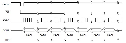
F28035 interfaces through SPI-B with a slave device. A low state in a Slave's pin indicates there's data to be read.
Then the 28035 must provide the clock signal, low the CS pin and read the slave's DOUT pin.

The data is 24 bit per word, having 7 words per read making a total of 168bits thread. Every thread is read 4,000 times /secc. The diagram below describes it:

Probelm:

I try to use the FIFO SPI code example in order to store 3 bytes of 8bits each one. That would have provided the equivalent to one word each time, but I couldn't make it work despite I tried a lot of different modifications in the code, including different register setups. I spent a lot of time trying to make this work.

I ended up reading 1 byte per byte but this is more time consuming.

Help needed.

I need a base code that allow me to read a set of 3 bytes from the Slave, because that will save precious time that would be used for calculations instead of SPI driving.

  • This is still pendient to be solved

  • Hello,

    I am not sure I can help.

    But maybe you can give your SPI snip code (initialization, interrupt, etc) so maybe somebody can check it and give you some input/idea.

    Good luck!

    Best regards,

    Maria

  • As Maria stated, can you share your SPI code (at least the initialization part) so that we can check for any mistakes.  

    You can also take a look at the TMS320F2703x SPI example in ControlSUITE to see if you missed something.  This code setups up the SPI for loopback.

    -Derek

  • HelLo Derek.
    
    
    The code was based on the SPI loopback interrupt example provided on TI's website.
    Some months ago I spent a lot of time trying this work with a buffer size of 3 for my application. I modified several registers in the SPI config, such as  SPICCR, SPICTL, SPISTS, SPIFFTX ,SPIFFRX. Also I tried different things in the ISR's. Once I gave up I just switched to a buffer size of 1 and made it work, of course I had to pay the processing time penalty.

    Thanks
    
    
    // TI File $Revision: /main/4 $
    // Checkin $Date: November 30, 2009   17:49:02 $
    //###########################################################################
    //
    // FILE:   Example_2803xSpi_FFDLB_int.c
    //
    // TITLE:  DSP2803x Device Spi Digital Loop Back with Interrupts Example.
    //
    // ASSUMPTIONS:
    //
    //    This program requires the DSP2803x header files.
    //
    //    This program uses the internal loop back test mode of the peripheral.
    //    Other then boot mode pin configuration, no other hardware configuration
    //    is required.
    //
    //    As supplied, this project is configured for "boot to SARAM"
    //    operation.  The 2803x Boot Mode table is shown below.
    //    For information on configuring the boot mode of an eZdsp,
    //    please refer to the documentation included with the eZdsp.
    //    $Boot_Table:
    //
    //    While an emulator is connected to your device, the TRSTn pin = 1,
    //    which sets the device into EMU_BOOT boot mode. In this mode, the
    //    peripheral boot modes are as follows:
    //
    //      Boot Mode:       EMU_KEY        EMU_BMODE
    //                       (0xD00)         (0xD01)
    //      ---------------------------------------
    //      Wait             !=0x55AA        X
    //      I/O              0x55AA          0x0000
    //      SCI              0x55AA          0x0001
    //      Wait             0x55AA          0x0002
    //      Get_Mode         0x55AA          0x0003
    //      SPI              0x55AA          0x0004
    //      I2C              0x55AA          0x0005
    //      OTP              0x55AA          0x0006
    //      eCANA            0x55AA          0x0007
    //      SARAM            0x55AA          0x000A   <-- "Boot to SARAM"
    //      Flash            0x55AA          0x000B
    //      Wait             0x55AA          Other
    //
    //   Write EMU_KEY to 0xD00 and EMU_BMODE to 0xD01 via the debugger
    //   according to the Boot Mode Table above. Build/Load project,
    //   Reset the device, and Run example
    //
    //   $End_Boot_Table
    //
    //
    // Description:
    //
    //    This program is a SPI-A example that uses the internal loopback of
    //    the peripheral.  Both interrupts and the SPI FIFOs are used.
    //
    //    A stream of data is sent and then compared to the recieved stream.
    //
    //    The sent data looks like this:
    //    0000 0001
    //    0001 0002
    //    0002 0003
    //    ....
    //    FFFE FFFF
    //    FFFF 0000
    //     etc..
    //
    //    This pattern is repeated forever.
    //
    //
    // Watch Variables:
    //     sdata[4]    - Data to send
    //     rdata[4]    - Received data
    //     rdata_point - Used to keep track of the last position in
    //                   the receive stream for error checking
    //###########################################################################
    //
    // Original Source by S.D.
    //
    // $TI Release: 2803x C/C++ Header Files V1.21 $
    // $Release Date: December 1, 2009 $
    //###########################################################################
    
    #include "DSP28x_Project.h"     // Device Headerfile and Examples Include File
    #include "DSP2803x_Device.h"
    #include "DSP2803x_Gpio.h"
    #include "math.h"
    
    // Prototype statements for functions found within this file.
    // interrupt void ISRTimer2(void);
    interrupt void spiTxFifoIsr(void);
    interrupt void spiRxFifoIsr(void);
    void delay_loop(void);
    void spi_fifo_init(void);
    void error();
    void SPITxDat();
    
    Uint16	sdata[35];		// Send data buffer
    Uint16	rdata[35];		// Receive data buffer
    Uint32	FixVect[8];		// Datos de entrada
    //Uint16 rdata_point;	// Keep track of where we are
    						// in the data stream to check received data
    Uint32	dat_buffer[601];
    //Uint32	dat_buffer2[601];
    
    char	SPIpointer;
    char	Tnsm;
    char	Iloop;
    int		word_cntr;  
    
    
    void main(void)
    {
    // Step 1. Initialize System Control:
    // PLL, WatchDog, enable Peripheral Clocks
    // This example function is found in the DSP2803x_SysCtrl.c file.
    	InitSysCtrl();
    
    // Step 2. Initalize GPIO:
    // This example function is found in the DSP2803x_Gpio.c file and
    // illustrates how to set the GPIO to it's default state.
    // InitGpio();  // Skipped for this example
    // Setup only the GP I/O only for SPI-A functionality
    	InitSpibGpio();
    	InitGpio();
    
    	GpioDataRegs.GPADAT.bit.GPIO10 = 0;		//ADC RESET
    	delay_loop();
    	GpioDataRegs.GPADAT.bit.GPIO11 = 0;		//ADC START_ADC --> Conversiones No ininciadas
    	delay_loop();
    	GpioDataRegs.GPADAT.bit.GPIO28 = 0;		//Señal de tiempo de ISR, en bajo.
    	delay_loop();
    	GpioDataRegs.GPADAT.bit.GPIO7 = 0;		//Pulso de prueba apagado
    	delay_loop();
    	GpioDataRegs.GPADAT.bit.GPIO6 = 0;		//Xtal externo en el ADC


    // Step 3. Initialize PIE vector table:
    // Disable and clear all CPU interrupts
    	DINT;
    	IER = 0x0000;
    	IFR = 0x0000;
    
    // Initialize PIE control registers to their default state:
    // This function is found in the DSP2803x_PieCtrl.c file.
       InitPieCtrl();
    
    // Initialize the PIE vector table with pointers to the shell Interrupt
    // Service Routines (ISR).
    // This will populate the entire table, even if the interrupt
    // is not used in this example.  This is useful for debug purposes.
    // The shell ISR routines are found in DSP2803x_DefaultIsr.c.
    // This function is found in DSP2803x_PieVect.c.
       InitPieVectTable();
    
    // Interrupts that are used in this example are re-mapped to
    // ISR functions found within this file.
       EALLOW;  // This is needed to write to EALLOW protected registers
       PieVectTable.SPIRXINTB = &spiRxFifoIsr;
       PieVectTable.SPITXINTB = &spiTxFifoIsr;
       EDIS;   // This is needed to disable write to EALLOW protected registers
    
    // Step 4. Initialize all the Device Peripherals:
    // This function is found in DSP2803x_InitPeripherals.c
    // InitPeripherals(); // Not required for this example
       spi_fifo_init();   // Initialize the SPI only
    
    // Step 5. User specific code, enable interrupts:
    
    
    // Copy time critical code and Flash setup code to RAM
    // InitFlash();
    // The  RamfuncsLoadStart, RamfuncsLoadEnd, and RamfuncsRunStart
    // symbols are created by the linker. Refer to the F2808.cmd file.
    	MemCopy(&RamfuncsLoadStart, &RamfuncsLoadEnd, &RamfuncsRunStart);
    
    // Call Flash Initialization to setup flash waitstates
    // This function must reside in RAM
    	InitFlash();
    
    // Enable interrupts required for this example
    	PieCtrlRegs.PIECTRL.bit.ENPIE = 1;   // Enable the PIE block
    	PieCtrlRegs.PIEIER6.bit.INTx3=1;     // Enable PIE Group 6, INT 3
    	PieCtrlRegs.PIEIER6.bit.INTx4=1;     // Enable PIE Group 6, INT 4
    	IER=0x20;                            // Enable CPU INT6
    	EINT;                                // Enable Global Interrupts
    	
    	word_cntr = 0xFFFF;
    
    	GpioDataRegs.GPADAT.bit.GPIO10 = 1;		//ADC RESET. ADC en Operación
    	delay_loop();
    	delay_loop();
    	delay_loop();
    	delay_loop();
    	GpioDataRegs.GPADAT.bit.GPIO10 = 0;		//ADC RESET
    	delay_loop();
    	GpioDataRegs.GPADAT.bit.GPIO10 = 1;		//ADC RESET. ADC en Operación
    	delay_loop();
    	sdata[0] = 0x1100;
    	sdata[1] = 0x0000;
    	sdata[2] = 0x0000;
    	sdata[3] = 0x0000;
    	SPIpointer = 0;
    	SPITxDat();								//SDATAC command
    	delay_loop();
    
    	sdata[0] = 0x4100;
    	sdata[1] = 0x0000;
    	//sdata[2] = 0xD400;
    	sdata[2] = 0x9400;
    	sdata[3] = 0x0000;
    	SPIpointer = 2;
    	SPITxDat();								//Data rate = 4kSPS, Config 1
    	delay_loop();
    
    	sdata[0] = 0x4200;
    	sdata[1] = 0x0000;
    	sdata[2] = 0xC000;
    	sdata[3] = 0x0000;
    	SPIpointer = 2;
    	SPITxDat();								//Config 2
    	delay_loop();
    
    	sdata[0] = 0x4300;
    	sdata[1] = 0x0000;
    	sdata[2] = 0xCC00;
    	sdata[3] = 0x0000;
    	SPIpointer = 2;
    	SPITxDat();								//Config 3
    	delay_loop();
    
    	for (Iloop = 0; Iloop <= 28; Iloop++)
        	{
        	sdata[Iloop] = 0;
    		rdata[Iloop] = 0;
        	}
    
    	char i;
        for (i = 0; i<=2; i++)
        		{
    			rdata[i]=SpibRegs.SPIRXBUF;     // Read data - Clean Buffer
        		}
    
    	sdata[0] = 0x2100;
    	sdata[1] = 0x0000;
    	sdata[2] = 0x0000;
    	sdata[3] = 0x0000;
    	SPIpointer = 2;
    	Tnsm = 0;
    	Iloop = 0;
    	SPITxDat();								//Leer Config 1
    	delay_loop();
    
    	GpioDataRegs.GPADAT.bit.GPIO11 = 1;		//ADC START_ADC --> Ininciar Conversiones
    	delay_loop();
    
    	sdata[0] = 0x1000;
    	sdata[1] = 0x0000;
    	sdata[2] = 0x0000;
    	sdata[3] = 0x0000;
    	SPIpointer = 0;
    	SPITxDat();								//RDATAC command
    
        Tnsm = 0;
        for (Iloop = 0; Iloop <= 28; Iloop++)
        	{
        	sdata[Iloop] = 0;
    		rdata[Iloop] = 0xFFFF;
        	}
    
    	int t;
    	for (t = 0; t<=600; t++)
    		{
    		dat_buffer[t] = 0;
    //		dat_buffer2[t] = 0;
    		}
    	word_cntr = 0;
    //	rdata[0]=SpibRegs.SPIRXBUF;
    	rdata[0]=0;
    	Iloop = 0;
    
    	//SPITxDat();
    // Step 6. IDLE loop. Just sit and loop forever (optional):
        for(;;)
        {
        GpioDataRegs.GPADAT.bit.GPIO28 = 0;
        if (GpioDataRegs.GPADAT.bit.GPIO5 == 0)
        	{
    	    	sdata[0] = 0;
    			sdata[1] = 0;
    			sdata[2] = 0;
    			sdata[3] = 0;
        		//SPIpointer = 26;
        		SPIpointer = 2;
        		Iloop = 0;
        		Tnsm = 1;
    			SPITxDat();
        	}
    	   	/*if (Tnsm ==1)
        		{
        		SPITxDat();
        		Tnsm = 0;
        		}*/
        }
    }
    
    // Some Useful local functions
    void delay_loop()
    {
        long      i;
        for (i = 0; i < 1000000; i++) {}
    }
    
    void error(void)
    {
        asm("     ESTOP0");  //Test failed!! Stop!
        for (;;);
    }
    
    void spi_fifo_init()
    {
    // Initialize SPI FIFO registers
       SpibRegs.SPICCR.bit.SPISWRESET=0; // Reset SPI
       
    
       SpibRegs.SPICCR.all=0x007;       //8-bit character
       SpibRegs.SPICTL.all=0x0017;       //Interrupt enabled, Master, Phase=0 (SPI int ena=1), talk=1,
       SpibRegs.SPISTS.all=0x0000;
       //SpibRegs.SPIBRR=0x0063;           // Baud rate
       SpibRegs.SPIBRR=0x0006;           // Baud rate
       //SpibRegs.SPIFFTX.all=0xC022;      // Enable FIFO's, set TX FIFO level to 4 ¿2? ----> This is confusing the example comment says 4 but writes "2"
       //SpibRegs.SPIFFRX.all=0x0022;      // Set RX FIFO level to 4 ¿2? ----> This is confusing the example comment says 4 but writes "2"
       SpibRegs.SPIFFTX.all=0xC023;      // Enable FIFO's, set TX FIFO level to 3, several values tried
       SpibRegs.SPIFFRX.all=0x0023;      // Set RX FIFO level to 3, several values tried
       SpibRegs.SPIFFCT.all=0x00;
       SpibRegs.SPIPRI.all=0x0010;
       SpibRegs.SPIFFTX.bit.TXFFIENA=0;  //On or Off depending on what it was tried
    
    	SpibRegs.SPICCR.bit.SPISWRESET=1;  // Enable SPI
    	
    	SpibRegs.SPIFFTX.bit.TXFIFO=1;
    	SpibRegs.SPIFFRX.bit.RXFIFORESET=1;
    }
    
    interrupt void spiTxFifoIsr(void)
    {
        SpibRegs.SPIFFTX.bit.TXFFINTCLR=1;  // Clear Interrupt flag
        PieCtrlRegs.PIEACK.all|=0x20;       // Issue PIE ACK
    }
    
    interrupt void spiRxFifoIsr(void)
    {
        char i;
        if (SpibRegs.SPIFFTX.bit.TXFFINT==1)
        	{
        	//for (i = 0; i<=SPIpointer; i++)
        	for (i = 0; i<=2; i++)
        		{
    			rdata[i+Iloop]=SpibRegs.SPIRXBUF;     // Read data
    			//rdata[i+Iloop]=SpibRegs.SPIDAT;     // Read data
    			//rdata[i+Iloop]=SpibRegs.SPIRXEMU;     // Read data
        		}
        	if (Iloop == 24)
        		{
        		Iloop = 0;
        		}
        	else
        		{
        		if (Tnsm ==1)
        			{
        			SPIpointer = 2;
    				SPITxDat();
        			}
        		}
        		i = Iloop/3;
       			//FixVect[i] = rdata[Iloop]+0x0100 * rdata[Iloop+1] + 0x010000 * rdata[Iloop+2];
       			//FixVect[i] = rdata[Iloop+2]+0x0100 * rdata[Iloop+1] + 0x010000 * rdata[Iloop];
       			FixVect[i] = 0x010000 * rdata[Iloop] +0x0100 * rdata[Iloop+1] + rdata[Iloop+2];
        		Iloop = Iloop +3;
        	if (word_cntr < 600)
        		{
        		dat_buffer[word_cntr] = FixVect[1];
        		word_cntr++;
        		}
        	/*if (word_cntr == 600)
        		{
        		word_cntr++;
        		word_cntr--;
        		}*/
        	/*else
        		{
        		if (word_cntr < 0xFFFF)
        			{
        			word_cntr--;
        			word_cntr++;
        			}
        		}*/
        	}
        SpibRegs.SPIFFRX.bit.RXFFOVFCLR=1;  // Clear Overflow flag
        SpibRegs.SPIFFRX.bit.RXFFINTCLR=1;  // Clear Interrupt flag
        PieCtrlRegs.PIEACK.all|=0x20;       // Issue PIE ack
    }
    
    void SPITxDat()
    {
    // Initalize the send data buffer
       	Uint16 Index;
        		/*for (Index = 0; Index<=SPIpointer; Index++)
        			{
        			//rdata[Index]=0;
        			SpibRegs.SPITXBUF=sdata[Index];      // Send data
        			}*/
        		for (Index = 0; Index<=SPIpointer; Index++)
        			{
        			//rdata[Index]=0;
        			SpibRegs.SPITXBUF=sdata[Index];      // Send data
        			}
    }


    //---------------------------------------------------------------------------
    // InitGpio:
    //---------------------------------------------------------------------------
    // This function initializes the Gpio to a known (default) state.
    //
    // For more details on configuring GPIO's as peripheral functions,
    // refer to the individual peripheral examples and/or GPIO setup example.
    void InitGpio(void)
    {
       EALLOW;
    
       // Each GPIO pin can be:
       // a) a GPIO input/output
       // b) peripheral function 1
       // c) peripheral function 2
       // d) peripheral function 3
       // By default, all are GPIO Inputs
    /*   GpioCtrlRegs.GPAMUX1.all = 0x0000;     // GPIO functionality GPIO0-GPIO15
       GpioCtrlRegs.GPAMUX2.all = 0x0000;     // GPIO functionality GPIO16-GPIO31
       GpioCtrlRegs.GPBMUX1.all = 0x0000;     // GPIO functionality GPIO32-GPIO44
       GpioCtrlRegs.AIOMUX1.all = 0x0000;     // Dig.IO funct. applies to AIO2,4,6,10,12,14
    
       GpioCtrlRegs.GPADIR.all = 0x0000;      // GPIO0-GPIO31 are GP inputs
       GpioCtrlRegs.GPBDIR.all = 0x0000;      // GPIO32-GPIO44 are inputs
       GpioCtrlRegs.AIODIR.all = 0x0000;      // AIO2,4,6,19,12,14 are digital inputs  */
    
       // Each input can have different qualification
       // a) input synchronized to SYSCLKOUT
       // b) input qualified by a sampling window
       // c) input sent asynchronously (valid for peripheral inputs only)
    /*   GpioCtrlRegs.GPAQSEL1.all = 0x0000;    // GPIO0-GPIO15 Synch to SYSCLKOUT
       GpioCtrlRegs.GPAQSEL2.all = 0x0000;    // GPIO16-GPIO31 Synch to SYSCLKOUT
       GpioCtrlRegs.GPBQSEL1.all = 0x0000;    // GPIO32-GPIO44 Synch to SYSCLKOUT   */
    
       // Pull-ups can be enabled or disabled.
    /*   GpioCtrlRegs.GPAPUD.all = 0x0000;      // Pullup's enabled GPIO0-GPIO31
       GpioCtrlRegs.GPBPUD.all = 0x0000;      // Pullup's enabled GPIO32-GPIO44    */
       //GpioCtrlRegs.GPAPUD.all = 0xFFFF;    // Pullup's disabled GPIO0-GPIO31
       //GpioCtrlRegs.GPBPUD.all = 0xFFFF;    // Pullup's disabled GPIO32-GPIO44
    
    	//Establecer como salidas los pines de control al ADC:
    	GpioCtrlRegs.GPADIR.bit.GPIO6 = 1;		//ADC CLKSEL
    	GpioCtrlRegs.GPADIR.bit.GPIO10 = 1;		//ADC RESET
    	GpioCtrlRegs.GPADIR.bit.GPIO11 = 1;		//ADC START_ADC
    	GpioCtrlRegs.GPADIR.bit.GPIO9 = 1;		//ADC PWDN
    	GpioCtrlRegs.GPADIR.bit.GPIO12 = 1;		//ADC DIN - TMS MOSIB
    	GpioCtrlRegs.GPADIR.bit.GPIO15 = 1;		//ADC CS
    	GpioCtrlRegs.GPADIR.bit.GPIO14 = 1;		//ADC SCLK
    	//GpioCtrlRegs.GPADIR.bit.GPIO11 = 1;		//QUEDA PENDIENTE UN PIN SCLK_SEL ADC
    
    	//Configurar como salidas los pines de led de prueba y monitoreo del DSP:
    	GpioCtrlRegs.GPADIR.bit.GPIO7 = 1;		//Pulso de Prueba
    	//GpioCtrlRegs.GPADIR.bit.GPIO18 = 1;		//Pulso de Prueba
    	GpioCtrlRegs.GPADIR.bit.GPIO28 = 1;		//Señal de tiempo de ISR
    
       EDIS;
    
    }
    
    
    void InitSpibGpio()
    {
       EALLOW;
    
    /* Enable internal pull-up for the selected pins */
    // Pull-ups can be enabled or disabled disabled by the user.
    // This will enable the pullups for the specified pins.
    // Comment out other unwanted lines.
    
        GpioCtrlRegs.GPAPUD.bit.GPIO12 = 0;     // Enable pull-up on GPIO12 (SPISIMOB)
    //  GpioCtrlRegs.GPAPUD.bit.GPIO24 = 0;     // Enable pull-up on GPIO24 (SPISIMOB)
    
        GpioCtrlRegs.GPAPUD.bit.GPIO13 = 0;     // Enable pull-up on GPIO13 (SPISOMIB)
    //  GpioCtrlRegs.GPAPUD.bit.GPIO25 = 0;     // Enable pull-up on GPIO25 (SPISOMIB)
    
        GpioCtrlRegs.GPAPUD.bit.GPIO14 = 0;     // Enable pull-up on GPIO14 (SPICLKB)
    //  GpioCtrlRegs.GPAPUD.bit.GPIO26 = 0;     // Enable pull-up on GPIO26 (SPICLKB)
    
        GpioCtrlRegs.GPAPUD.bit.GPIO15 = 0;     // Enable pull-up on GPIO15 (SPISTEB)
    //  GpioCtrlRegs.GPAPUD.bit.GPIO27 = 0;     // Enable pull-up on GPIO27 (SPISTEB)
    
    
    /* Set qualification for selected pins to asynch only */
    // This will select asynch (no qualification) for the selected pins.
    // Comment out other unwanted lines.
    
        GpioCtrlRegs.GPAQSEL1.bit.GPIO12 = 3;   // Asynch input GPIO12 (SPISIMOB)
    //  GpioCtrlRegs.GPAQSEL2.bit.GPIO24 = 3;   // Asynch input GPIO24 (SPISIMOB)
    
        GpioCtrlRegs.GPAQSEL1.bit.GPIO13 = 3;   // Asynch input GPIO13 (SPISOMIB)
    //  GpioCtrlRegs.GPAQSEL2.bit.GPIO25 = 3;   // Asynch input GPIO25 (SPISOMIB)
    
        GpioCtrlRegs.GPAQSEL1.bit.GPIO14 = 3;   // Asynch input GPIO14 (SPICLKB)
    //  GpioCtrlRegs.GPAQSEL2.bit.GPIO26 = 3;   // Asynch input GPIO26 (SPICLKB)
    
    /*    GpioCtrlRegs.GPAQSEL1.bit.GPIO15 = 3;   // Asynch input GPIO15 (SPISTEB)*/
    //  GpioCtrlRegs.GPAQSEL2.bit.GPIO27 = 3;   // Asynch input GPIO27 (SPISTEB)
    
    /* Configure SPI-B pins using GPIO regs*/
    // This specifies which of the possible GPIO pins will be SPI functional pins.
    // Comment out other unwanted lines.
    
        GpioCtrlRegs.GPAMUX1.bit.GPIO12 = 3;    // Configure GPIO12 as SPISIMOB
    //  GpioCtrlRegs.GPAMUX2.bit.GPIO24 = 3;    // Configure GPIO24 as SPISIMOB
    
        GpioCtrlRegs.GPAMUX1.bit.GPIO13 = 3;    // Configure GPIO13 as SPISOMIB
    //  GpioCtrlRegs.GPAMUX2.bit.GPIO25 = 3;    // Configure GPIO25 as SPISOMIB
    
        GpioCtrlRegs.GPAMUX1.bit.GPIO14 = 3;    // Configure GPIO14 as SPICLKB
    //  GpioCtrlRegs.GPAMUX2.bit.GPIO26 = 3;    // Configure GPIO26 as SPICLKB
    
    /*    GpioCtrlRegs.GPAMUX1.bit.GPIO15 = 3;    // Configure GPIO15 as SPISTEB*/
    //  GpioCtrlRegs.GPAMUX2.bit.GPIO27 = 3;    // Configure GPIO27 as SPISTEB
    
        EDIS;
    }
    #endif //endif DSP28_SPIB
    
    //===========================================================================
    // End of file.
    //===========================================================================


    //===========================================================================
    // No more.
    //===========================================================================


  • This is being discussed offline.