This thread has been locked.

If you have a related question, please click the "Ask a related question" button in the top right corner. The newly created question will be automatically linked to this question.

Configuration ADC and GPIO F28027

Other Parts Discussed in Thread: CONTROLSUITE, LAUNCHXL-F28027F

Hello guys.

I'm starting at piccolo f28027. I've learned to light some leds with
some didactic.

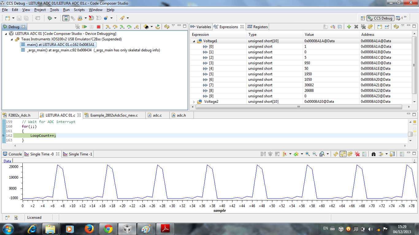
At this point, I would like to insert a square wave in ADC, and show that the output signal, an LED lighting and extinguishing the GPIO 0.
The input signal has an offset of 1V. Subtract a value from the ADC (4095/3.3) relative to 1V, and compare it to zero.

Already configured the ADC and GPIO, but I can not get the desired result.

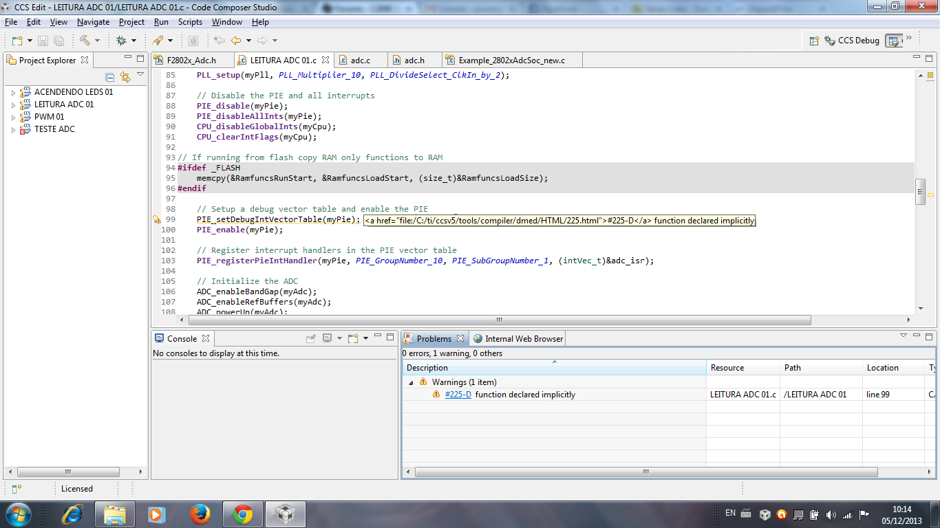
And In expressions, I do not see the value of the variable. Generates an error.

Could anyone help me?

Thank you.

This is the code I used

/*
* main.c
*/
#include <stdio.h>
#include <file.h>

#include "DSP28x_Project.h" // DSP28x Headerfile

#include "f2802x_common/include/adc.h"
#include "f2802x_common/include/clk.h"
#include "f2802x_common/include/gpio.h"
#include "f2802x_common/include/pie.h"
#include "f2802x_common/include/pll.h"
#include "f2802x_common/include/wdog.h"

interrupt void adc_isr(void);

//#ifdef _FLASH
// memcpy(&RamfuncsRunStart, &RamfuncsLoadStart, (size_t)&RamfuncsLoadSize);
//#endif


int16 SaidaAdc;
int16 Tensao;

ADC_Handle myAdc;
CLK_Handle myClk;
GPIO_Handle myGpio;

PWM_Handle myPwm;


void main()
{
CPU_Handle myCpu;
WDOG_Handle myWDog;
PLL_Handle myPll;

myAdc = ADC_init((void *)ADC_BASE_ADDR, sizeof(ADC_Obj));
myClk = CLK_init((void *)CLK_BASE_ADDR, sizeof(CLK_Obj));
myCpu = CPU_init((void *)NULL, sizeof(CPU_Obj));
myGpio = GPIO_init((void *)GPIO_BASE_ADDR, sizeof(GPIO_Obj));

myPll = PLL_init((void *)PLL_BASE_ADDR, sizeof(PLL_Obj));
myPwm = PWM_init((void *)PWM_ePWM1_BASE_ADDR, sizeof(PWM_Obj));
myWDog = WDOG_init((void *)WDOG_BASE_ADDR, sizeof(WDOG_Obj));

// Perform basic system initialization
WDOG_disable(myWDog);
CLK_enableAdcClock(myClk);

//Select the internal oscillator 1 as the clock source
CLK_setOscSrc(myClk, CLK_OscSrc_Internal);

// Setup the PLL for x12 /2 which will yield 60Mhz = 10Mhz * 12 / 2
PLL_setup(myPll, PLL_Multiplier_12, PLL_DivideSelect_ClkIn_by_2);

// Disable the PIE and all interrupts

CPU_disableGlobalInts(myCpu);
CPU_clearIntFlags(myCpu);


//INICIALIZAÇÃO E CONFIGURAÇÃO DO GPIO

myGpio = GPIO_init((void *)GPIO_BASE_ADDR, sizeof(GPIO_Obj));

GPIO_setMode(myGpio, GPIO_Number_0, GPIO_0_Mode_GeneralPurpose);
GPIO_setDirection(myGpio, GPIO_Number_0, GPIO_Direction_Output);
GPIO_setMode(myGpio, GPIO_Number_1, GPIO_1_Mode_GeneralPurpose);
GPIO_setDirection(myGpio, GPIO_Number_1, GPIO_Direction_Output);
GPIO_setMode(myGpio, GPIO_Number_2, GPIO_2_Mode_GeneralPurpose);
GPIO_setDirection(myGpio, GPIO_Number_2, GPIO_Direction_Output);
GPIO_setMode(myGpio, GPIO_Number_3, GPIO_3_Mode_GeneralPurpose);
GPIO_setDirection(myGpio, GPIO_Number_3, GPIO_Direction_Output);


//INICIALIZAÇÃO E CONFIGURAÇÃO DO ADC
ADC_enableBandGap(myAdc);
ADC_enableRefBuffers(myAdc);
ADC_powerUp(myAdc);
ADC_enable(myAdc);
ADC_setVoltRefSrc(myAdc, ADC_VoltageRefSrc_Int);

//ADC_setIntPulseGenMode(myAdc, ADC_IntPulseGenMode_Prior);
// AdcRegs.INTSEL1N2.bit.INT1E = 1; //Enabled ADCINT1

ADC_enableInt(myAdc, ADC_IntNumber_1);
// AdcRegs.INTSEL1N2.bit.INT1CONT = 0; //Disable ADCINT1 Continuous mode

ADC_setIntMode(myAdc, ADC_IntNumber_1, ADC_IntMode_ClearFlag);
// AdcRegs.INTSEL1N2.bit.INT1SEL = 1; //setup EOC1 to trigger ADCINT1 to fire

ADC_setIntSrc(myAdc, ADC_IntNumber_1, ADC_IntSrc_EOC1);
// AdcRegs.ADCSOC0CTL.bit.CHSEL = 5; //set SOC0 channel select to ADCINA5 (which is internally connected to the temperature sensor)

ADC_setSocChanNumber (myAdc, ADC_SocNumber_0, ADC_SocChanNumber_A1);


ADC_setSocSampleWindow(myAdc, ADC_SocNumber_0, ADC_SocSampleWindow_7_cycles);

//}
// PROGRAMA

// GPIO_setHigh(myGpio, GPIO_Number_0);
// GPIO_setHigh(myGpio, GPIO_Number_1);
// GPIO_setHigh(myGpio, GPIO_Number_2);
// GPIO_setHigh(myGpio, GPIO_Number_3);

while(1)
{
SaidaAdc = ADC_readResult(myAdc, ADC_ResultNumber_1);
Tensao = SaidaAdc-1241;

if(Tensao >= 0)
{
GPIO_setHigh(myGpio, GPIO_Number_0);
}
else
GPIO_setLow(myGpio, GPIO_Number_0);

}


}

  • Hi,

    The input signal has an offset of 1V. Subtract a value from the ADC (4095/3.3) relative to 1V, and compare it to zero.

    The above statement is very unclear and generating a square wave would be easier using PWM. Anyways back to your point: first of all are your ADC routines working properly ? Are you getting valid ADC values?

    Regards,

    Gautam

  • Hi

    I believe that the routines are running ADC yes, based on existing examples in controlSUITE.

    If the ADC is reading or not, I do not know. I think you're missing a line of code, but do not know where.

  • HI,

    If the ADC is reading or not, I do not know.

    Check the reading on the watch window and try to plot a graph.

    Regards,

    Gautam

  • Hello Patrick,

    What is inside
    ADC_enableInt(myAdc, ADC_IntNumber_1); ?
    Is it the one in adc.c?

    If so, then in which lines do you enable pie and global interrupt?

    You can refer again Example_F2802xAdcSoc from controlSuite.


    Best regards,
    Maria

  • Hi Gautam

    In the watch window the ADC has zero value.

    In the graph, nothing appears.

    Does the ADC is performing only one reading?

  • Hi Maria

    I would like to try to accomplish this example without using

    interruptions. Is it possible?. For as I am learning, still do not quite understand the

    interruptions. 


  • Hello Patrick,

    Because you said you are still learning, I suggest you to try first the example from ControlSuite (without modifying it) and try to understand it before moving to your code.

    The example will help you a lot to understand about ADC. And then you can remove the interrupt part.

    Also please read the documentation of F28027 to compare with the example, so you will know which one is for interrupt and which one is not.

    Best regards,

    Maria

  • Hi Maria.

    Ahh yes. Thanks for the suggestion. Yeah I'll look in the example shown. Ja could download the manual ADC also.

    Thank you for your help.

  • Hi Patrick,

    When on continuous debug run, the values should be floating (when no input is given); else the ADC is not configured properly. If ADC value =0, then check whether the ADC pin is not grounded.

    Also, as Maria has suggested, please go through the sample codes first, understand them and their concepts thoroughly and only then move forward.

    Regards,

    Gautam

  • Hello Gautam and Mary.

    I gave one example studied in Tempsoc.

    I ran the program ready, without connecting any signal at the ADC input, and yet it seems that the ADC is reading.

    Then connected one sinusoidal signal at the ADC input A2 and A4, but the ADC showed the same values ​​for the case without signal.

    So I think that the ADC is not reading anything, just noise. I do not understand, because the program is not providing input signals in the ADCIN4 ADCIN2?

    best regards

  • Hello Patrick,

    Which example code is that?

    Is it Example_F2802xAdcTempSensor?

    In this example, it uses ADCINA5, which is internally connected to the temperature sensor (so you don't need to give any input).

    If you try this example, can you debug TempSensorVoltage[] in adc_isr()? You should get some value.

    Best regards,

    Maria

  • Hi Maria,

    Is not example of the temperature sensor.

    It is: Example_2802xAdcSoc.c. which he sets as input the ADCINA2 and ADCINA4 (Voltage1 and Voltage2).

    In the example F2802xAdcTempSensor, you mentioned, if I switch ADCINA5 to ADCINA2 and put a sign on the ADCINA2 should or should not work? Well I tried that too but did not succeed.

    best regards

  • Hello Patrick,

    In Example_2802xAdcSoc.c, you don't need to input anything since the input will be from PWM.

    In this case, what is the result of Voltage1 and Voltage2 in your debugger?

    For example F2802xAdcTempSensor, you cannot change ADCINA5 to ADCINA2 just like that (ADCINA2 doesn't connect to temperature sensor internally). You need to change some other ADC registers too.

    Best regards,

    Maria

  • Hi Maria

    In the example F280x Adcsoc.c outputs are:

    Voltage1: [202 35079 64129 22944 49598 51855 32651 62421 35919 26861]
    Voltage2: [60687 9763 42547 520 18010 29076 39901 41080 61090 59472]

    Now I tested again, and the values ​​of voltage2 changed.
    Voltage2: [30717 30717 63 63 0 0 0 0 61154 59393]

    So in this example F280x Adcsoc.c not need to connect any input signal, the input is already the PWM? As the AdcINA4 and AdcINA2 reads if you have nothing connected them? I do not understand this.

    What if I want to connect a signal in AdcINA2, for example, from a function generator and read with AdcINA2 as I do? Examples of temperature sensor I had understood it was already enabled Adc input for an external, but by the way is not, right?

    Best regards.

  • Hi Maria

    Does the fact that the program Adcsoc. do not read anything when I connect an input signal in ADCINA2 or ADCINA4's because the internal reference voltage to be enabled (bandgap)? Does the ADC is reading a voltage generated internally to the DSP?

    Was studying the ADC and found two configuration options: mode voltage reference with internal or external.

    What do you think?

    Best regards.

    Patrick.

  • Hi Patrick,

    As the example you're working on is dependent on the PWM duty cycle (as a DAC); why dont you try with Example_2802xAdcTempSensor. This would give you desired results.

    Regards,

    Gautam

  • Hello Patrick,

    Did you try the example of ADC Temp Sensor? What is your TempSensorVoltage result?

    About Voltage1 and Voltage2, since this is 12-bit ADC, i think the result should not be more than 4095 (please somebody correct me if I am wrong). So I don't have any idea why it is so difficult to run this example like expected for you.

    Have you ever modified something for F28027 codes? Maybe the clock configuration or something else?

    Actually I have never tried the example code of F28027 yet.

    But I will get LaunchXL-F28027F. I will try it when I get it (but it will be a week or more).

    Best regards,

    Maria

  • Hello again,

    About the voltage reference, internally or not, it is used as reference.

    The ADC uses this voltage reference as scale range.

     From the datasheet:

    I have looked again the AdcSoc example::

    The SOC (start of conversion) occurs every PWM clock (SOC0 and SOC1 - read ADCINA4, SOC2 - read ADCINA2, eavery PWM clock)

    ADC interrupt (ADCINT1) occurs every EOC2 (end of conversion of SOC 2). But it will not occur if the interrupt flag is not clear.

    So seems that PWM clock only starts the SOC.

    Will you do a favor,

    1. try example AdcSoc but connect ADCINA4 and ADCINA2 to GND. What are the results of Voltage1 and Voltage2?

    1. try example AdcSoc but connect ADCINA4 and ADCINA2 to 3.3V. What are the results of Voltage1 and Voltage2?

    Best regards,

    Maria

  • Hi Maria
     
    I connected the ADCINA4 ADCINA2 and the GND and then at 3.3 V. The results are the same.

    Voltage1 [35079 202 31361 22944 49598 51855 32651 30677 35919 26861]
    Voltage2 [59183 9763 42539 520 18010 29076 39901 41080 61154 59392]

    I agree with you, the ADC values ​​should not exceed 4095.

    In my opinion, I think the ADC is programmed to read something internal that should be disabled and so Unlockable input pins. But if it's happening really, I do not know to solve. I thought the example was ready for a reading of data connected to pins of the ADC.

    Best regards,

    Patrick.

  • And how about TempSensor example?

    Did you try it?

    Best regards,

    Maria

  • Hi Maria

    I've tried too, but to no avail. The results are always the same regardless of the input.

    Best regards,

    Patrick

  • Hello Patrick,

    This is not normal. Maybe hardware problem.

    Did you try blinking leds before? with timer  and no timer?

    Did they work?

    Is there any switch to be set?

    Please check the voltage of your board and MCU too.

    Best regards,

    Maria

  • Hello Maria

    I was set to make the LEDs light up.

    However, I still have not read any signal with the ADC. I believe it is not hardware problem or tension, but programming. Ainad probably lack some definition, some command, some line of code that activates the ADC.

    I'm still looking at the problem, because I need to make it work.

    Thanks for the help so far.

    If I can find the error, post here the problem and the solution.

    Best regards

  • Patrick,

      I am sorry you are having so much trouble with getting expected results using the ADC.  I definitely think you were on the right track to use the adc_soc example and drive the converting channels to GND/VDDIO.  One question I have is whether you are stopping at a breakpoint or halting the code to view to contents of Voltage1 and Voltage2?  In CCS the registers and memory locations will not update while code is running (by default), so they may appear to contain random information until the device is halted.

      Also did you mention whether you are using custom hardware or TI control card or development kit?  I see you are moving away from it being a hardware issue, but the example should work on TI hardware as long as you drive the inputs.

    regards, Joe

  • Hello Patrick,

    I think I found what it is wrong in ADC of F28027.

    I really hope it is the problem.

    In adc.h, ADCCTL2 definition is missing. And the fact we need it to set up CLKDIV bit.

    So I attach the modification files here.

    2742.adc-f28027.zip

    The modifications are:

    ADC.H

    //! \brief Defines the location of the CLKDIV2EN bits in the ADCTL2 register
    //!
    #define ADC_ADCCTL2_CLKDIV2EN_BITS         (1 << 0)

    //! \brief Defines the location of the ADCNONOVERLAP bits in the ADCTL2 register
    //!
    #define ADC_ADCCTL2_ADCNONOVERLAP_BITS      (1 << 1)

    //! \brief Defines the analog-to-digital converter (ADC) object
    //!
    typedef struct _ADC_Obj_
    {
        volatile uint16_t      ADCRESULT[16];    //!< ADC result registers
        volatile uint16_t      resvd_1[26096];   //!< Reserved
        volatile uint16_t      ADCCTL1;          //!< ADC Control Register 1
        volatile uint16_t      ADCCTL2;
        //volatile uint16_t      rsvd_2[3];        //!< Reserved
        volatile uint16_t      rsvd_2[2];        //!< Reserved
        volatile uint16_t      ADCINTFLG;        //!< ADC Interrupt Flag Register
        volatile uint16_t      ADCINTFLGCLR;     //!< ADC Interrupt Flag Clear Register
        volatile uint16_t      ADCINTOVF;        //!< ADC Interrupt Overflow Register
        volatile uint16_t      ADCINTOVFCLR;     //!< ADC Interrupt Overflow Clear Register
        volatile uint16_t      INTSELxNy[5];     //!< ADC Interrupt Select x and y Register
        volatile uint16_t      rsvd_3[3];        //!< Reserved
        volatile uint16_t      SOCPRICTRL;       //!< ADC Start Of Conversion Priority Control Register
        volatile uint16_t      rsvd_4;           //!< Reserved
        volatile uint16_t      ADCSAMPLEMODE;    //!< ADC Sample Mode Register
        volatile uint16_t      rsvd_5;           //!< Reserved
        volatile uint16_t      ADCINTSOCSEL1;    //!< ADC Interrupt Trigger SOC Select 1 Register
        volatile uint16_t      ADCINTSOCSEL2;    //!< ADC Interrupt Trigger SOC Select 2 Register
        volatile uint16_t      rsvd_6[2];        //!< Reserved
        volatile uint16_t      ADCSOCFLG1;       //!< ADC SOC Flag 1 Register
        volatile uint16_t      rsvd_7;           //!< Reserved
        volatile uint16_t      ADCSOCFRC1;       //!< ADC SOC Force 1 Register
        volatile uint16_t      rsvd_8;           //!< Reserved
        volatile uint16_t      ADCSOCOVF1;       //!< ADC SOC Overflow 1 Register
        volatile uint16_t      rsvd_9;           //!< Reserved
        volatile uint16_t      ADCSOCOVFCLR1;    //!< ADC SOC Overflow Clear 1 Register
        volatile uint16_t      rsvd_10;          //!< Reserved
        volatile uint16_t      ADCSOCxCTL[16];   //!< ADC SOCx Control Registers
        volatile uint16_t      rsvd_11[16];      //!< Reserved
        volatile uint16_t      ADCREFTRIM;       //!< ADC Reference/Gain Trim Register
        volatile uint16_t      ADCOFFTRIM;       //!< ADC Offset Trim Register
        volatile uint16_t      resvd_12[13];     //!< Reserved
        volatile uint16_t      ADCREV;           //!< ADC Revision Register
    } ADC_Obj;

    //! \brief Enumeration to define the start of conversion (SOC) numbers
    //!
    typedef enum
    {
      ADC_DivideSelect_ClkIn_by_1=0,                     //!< Denotes Main Clock Prescaling of 0
      ADC_DivideSelect_ClkIn_by_2=1                      //!< Denotes Main Clock Prescaling of 2
    } ADC_DivideSelect_e;


    //! \brief     Enables no overlap mode
    //! \param[in] adcHandle  The analog-to-digital converter (ADC) object handle
    void ADC_enableNoOverlapMode(ADC_Handle adcHandle);


    //! \brief     Sets the analog-to-digital converter (ADC) divide select value
    //! \param[in] adcHandle    The analog-to-digital converter (ADC) object handle
    //! \param[in] divSelect    The scale reference source
    void ADC_setDivideSelect(ADC_Handle adcHandle,const ADC_DivideSelect_e divSelect);


    ADC.C


    void ADC_enableNoOverlapMode(ADC_Handle adcHandle)
    {
      ADC_Obj *adc = (ADC_Obj *)adcHandle;


      ENABLE_PROTECTED_REGISTER_WRITE_MODE;

      // set the bits
      adc->ADCCTL2 |= ADC_ADCCTL2_ADCNONOVERLAP_BITS;

      DISABLE_PROTECTED_REGISTER_WRITE_MODE;

      return;
    } // end of ADC_enableNoOverlapMode() function

    void ADC_setDivideSelect(ADC_Handle adcHandle,const ADC_DivideSelect_e divSelect)
    {
      ADC_Obj *adc = (ADC_Obj *)adcHandle;


      ENABLE_PROTECTED_REGISTER_WRITE_MODE;

      // clear the bits
      adc->ADCCTL2 &= (~(ADC_ADCCTL2_CLKDIV2EN_BITS));


      // set the bits
      adc->ADCCTL2 |= divSelect;

      DISABLE_PROTECTED_REGISTER_WRITE_MODE;

      return;
    } // end of ADC_setDivideSelect() function


    EXAMPLE_2802xAdcSoc.C


        ADC_setDivideSelect(myAdc, ADC_DivideSelect_ClkIn_by_2); // put it in initialization, before main loop

    Please replace adc.h, adc.c, and example_2802xAdcSoc.c files using the ones that I send.

    Please try it (by connected to GND or VDD) and let us know the result.

    You can use ADC_enableNoOverlapMode also to avoid overlap sample.

    Best regards,

    Maria

  • The fact, this register ADCCTL2 is not available for revision 0 silicon.

    So I don't know whether this is the source of the problem or not.

    And I haven't succeed to build the example project with the modification.

    I removed driverlib.lib from example project and added necessary files but still can't get rid of some errors.

    Let see.

    Updated: Finally I can get rid the error by changing the project back to use driverlib.lib but I put

    void ADC_enableNoOverlapMode(ADC_Handle adcHandle)
    {
      ADC_Obj *adc = (ADC_Obj *)adcHandle;


      ENABLE_PROTECTED_REGISTER_WRITE_MODE;

      // set the bits
      adc->ADCCTL2 |= ADC_ADCCTL2_ADCNONOVERLAP_BITS;

      DISABLE_PROTECTED_REGISTER_WRITE_MODE;

      return;
    } // end of ADC_enableNoOverlapMode() function

    void ADC_setDivideSelect(ADC_Handle adcHandle,const ADC_DivideSelect_e divSelect)
    {
      ADC_Obj *adc = (ADC_Obj *)adcHandle;


      ENABLE_PROTECTED_REGISTER_WRITE_MODE;

      // clear the bits
      adc->ADCCTL2 &= (~(ADC_ADCCTL2_CLKDIV2EN_BITS));


      // set the bits
      adc->ADCCTL2 |= divSelect;

      DISABLE_PROTECTED_REGISTER_WRITE_MODE;

      return;
    } // end of ADC_setDivideSelect() function

    in EXAMPLE_2802xAdcSoc.C instead of ADC.C

    Best regards,

    Maria

  • Hi Maria.

    Insert the files you sent me and ran the program.

    The ADC is still not reading what is on the input pins A4 or A2. connected the

    A4 and A2 pins GND and Vcc on, however, the read values ​​are not in accordance with the

    entry.

    I have a question: How do I know that the command ADC_readResult (myAdc,

      ADC_ResultNumber_1) ouADC_readResult (myAdc, ADC_ResultNumber_2)

      is reading or ADCINA4 ADCINA2? Which line of code that tells me this?

    The following are the results:

    Note that there is a warning related to PIE:

    I can not tell if this warning may cause measurement errors of the ADC

    Thanks for all the help.

    Best Reagards

  • Hello Patrick,

    For eliminate that warning, you can define _DEBUG in the project properties.

    About your question, I don't quite understand what you meant.

    In the example code AdcSoc, these lines:

     ADC_setSocChanNumber (myAdc, ADC_SocNumber_1, ADC_SocChanNumber_A4);    //set SOC1 channel select to ADCINA4
        ADC_setSocChanNumber (myAdc, ADC_SocNumber_2, ADC_SocChanNumber_A2);    //set SOC2 channel select to ADCINA2

    are used to set channel 1 to ADCINA4, and channel 2 to ADCINA2.

    Then in the ADC interrupt:

     Voltage1[ConversionCount] = ADC_readResult(myAdc, ADC_ResultNumber_1);
     Voltage2[ConversionCount] = ADC_readResult(myAdc, ADC_ResultNumber_2);

    Voltage 1 is assigned as the result of ADC channel 1.

    Voltage 2 is assigned as the result of ADC channel 2.

    So by reading Voltage 1 and Voltage 2, we can get ADC result 1 and 2 that came from ADCINA4 and ADCINA2 (but in your case, we don't know why the results are strange).

    About ADC_readResult, you can find it in adc.h

    //! \brief     Reads the specified ADC result (i.e. value)
    //! \param[in] adcHandle     The ADC handle
    //! \param[in] resultNumber  The result number for the ADCRESULT registers
    //! \return    The ADC result
    inline uint_least16_t ADC_readResult(ADC_Handle adcHandle, const ADC_ResultNumber_e resultNumber)
    {
        ADC_Obj *adc = (ADC_Obj *)adcHandle;

        return(adc->ADCRESULT[resultNumber]);
    } // end of ADC_read() function

    Really hope you can solve your problem.

    PS: I still have not gotten my launchxl yet from my manager so I still can't try it by myself.

    Best regards,

    Maria

  • One thing I want to ask:

    Did you press this button below ?

    This button is used to get continuous data (refresh the data) while debugging.

    Best regards,

    Maria

  • Hello Patrick,

    Suddenly this thread (from 2012) appeared today,

    http://e2e.ti.com/support/microcontrollers/c2000/f/171/t/234387.aspx

    and I found these lines from TI expert:

    The issue is that we are missing the line of code to start the PWM:
    CLK_enableTbClockSync(myClk);
    which should be placed just before the forever for() loop.

    I don't know they have fixed this yet or not but I could not find this line in the example.

    Well, in this case, you can add InitSysCtrl() to make sure the system control initialization is written:

    myAdc = ADC_init((void *)ADC_BASE_ADDR, sizeof(ADC_Obj));
    myClk = CLK_init((void *)CLK_BASE_ADDR, sizeof(CLK_Obj));

    .....

    InitSysCtrl();

    .....

    And add F2802x_SysCtrl.c to your project.

    I really hope this helps because I want to use F28027 too so I don't want to face this kind of problem too later.

    Best regards,

    Maria

  • Hello Maria

    It worked. ADCINA4 and connected the GND and Vcc ADCINA2 in and it worked. reading

    4095 and 0 respectively.

    After I performed other tests: I realized that those files you modified not

    are needed to change because I returned the original files and also ran.

    Now, the changes you made ​​should count for something yes. as

    I'm still learning, I can not say when such modifications will be necessary.

    The secret was to add even just the command: CLK_enableTbClockSync (myClk);

    / /! \ brief Enables the team ePWM module base clock sync signal.

    I'll be doing some more tests to make sure that is funcinando and send you the

    code.

    Thank you so much for all your help and patience and disposition.

    Best regards

  • Hello Patrick,

    I am really glad your code has worked.

    Please do share your result, maybe somebody else will need it later.

    Have nice days!

    Best regards,

    Maria

  • Oi Maria

    Follow the code.

    Thank you again.

    Best regards.

    //#############################################################################
    //
    // File: f2802x_examples_ccsv4/adc_soc/Example_F2802xAdcSoc.c
    //
    // Title: F2802x ADC Start-Of-Conversion (SOC) Example Program.
    //
    // Group: C2000
    // Target Device: TMS320F2802x
    //
    //! \addtogroup example_list
    //! <h1>ADC Start-Of-Conversion (SOC)</h1>
    //!
    //! Interrupts are enabled and the ePWM1 is setup to generate a periodic
    //! ADC SOC - ADCINT1. Two channels are converted, ADCINA4 and ADCINA2.
    //!
    //! Watch Variables:
    //!
    //! - Voltage1[10] - Last 10 ADCRESULT0 values
    //! - Voltage2[10] - Last 10 ADCRESULT1 values
    //! - ConversionCount - Current result number 0-9
    //! - LoopCount - Idle loop counter
    //
    // (C) Copyright 2012, Texas Instruments, Inc.
    //#############################################################################
    // $TI Release: f2802x Support Library v200 $
    // $Release Date: Tue Jul 24 10:01:39 CDT 2012 $
    //#############################################################################

    #include "DSP28x_Project.h" // Device Headerfile and Examples Include File

    #include "f2802x_common/include/adc.h"
    #include "f2802x_common/include/clk.h"
    #include "f2802x_common/include/flash.h"
    #include "f2802x_common/include/gpio.h"
    #include "f2802x_common/include/pie.h"
    #include "f2802x_common/include/pll.h"
    #include "f2802x_common/include/wdog.h"

    // Prototype statements for functions found within this file.
    interrupt void adc_isr(void);
    void Adc_Config(void);

    // Configure the period for each timer
    #define EPWM1_MIN_CMPA 1000 // Period register

    // Global variables used in this example:
    uint16_t LoopCount;
    uint16_t ConversionCount;
    uint16_t Voltage1[10];
    uint16_t Voltage2[10];

    ADC_Handle myAdc;
    CLK_Handle myClk;
    FLASH_Handle myFlash;
    GPIO_Handle myGpio;
    PIE_Handle myPie;
    PWM_Handle myPwm;

    //unsigned int resultcounter = 0;

    void main(void)
    {

    CPU_Handle myCpu;
    PLL_Handle myPll;
    WDOG_Handle myWDog;

    // Initialize all the handles needed for this application
    myAdc = ADC_init((void *)ADC_BASE_ADDR, sizeof(ADC_Obj));
    myClk = CLK_init((void *)CLK_BASE_ADDR, sizeof(CLK_Obj));
    myCpu = CPU_init((void *)NULL, sizeof(CPU_Obj));
    myFlash = FLASH_init((void *)FLASH_BASE_ADDR, sizeof(FLASH_Obj));
    myGpio = GPIO_init((void *)GPIO_BASE_ADDR, sizeof(GPIO_Obj));
    myPie = PIE_init((void *)PIE_BASE_ADDR, sizeof(PIE_Obj));
    myPll = PLL_init((void *)PLL_BASE_ADDR, sizeof(PLL_Obj));
    myPwm = PWM_init((void *)PWM_ePWM1_BASE_ADDR, sizeof(PWM_Obj));
    myWDog = WDOG_init((void *)WDOG_BASE_ADDR, sizeof(WDOG_Obj));


    // Perform basic system initialization
    WDOG_disable(myWDog);
    CLK_enableAdcClock(myClk);
    (*Device_cal)();

    //Select the internal oscillator 1 as the clock source
    CLK_enableTbClockSync(myClk);
    CLK_setOscSrc(myClk, CLK_OscSrc_Internal);

    // Setup the PLL for x10 /2 which will yield 50Mhz = 10Mhz * 10 / 2
    PLL_setup(myPll, PLL_Multiplier_10, PLL_DivideSelect_ClkIn_by_2);

    // Disable the PIE and all interrupts
    PIE_disable(myPie);
    PIE_disableAllInts(myPie);
    CPU_disableGlobalInts(myCpu);
    CPU_clearIntFlags(myCpu);

    // If running from flash copy RAM only functions to RAM
    #ifdef _FLASH
    memcpy(&RamfuncsRunStart, &RamfuncsLoadStart, (size_t)&RamfuncsLoadSize);
    #endif


    // Initalize GPIO
    GPIO_setPullUp(myGpio, GPIO_Number_0, GPIO_PullUp_Disable);
    GPIO_setMode(myGpio, GPIO_Number_0, GPIO_0_Mode_EPWM1A);

    // Setup a debug vector table and enable the PIE
    PIE_setDebugIntVectorTable(myPie);
    PIE_enable(myPie);

    // Register interrupt handlers in the PIE vector table
    PIE_registerPieIntHandler(myPie, PIE_GroupNumber_10, PIE_SubGroupNumber_1, (intVec_t)&adc_isr);

    // Initialize the ADC
    ADC_enableBandGap(myAdc);
    ADC_enableRefBuffers(myAdc);
    ADC_powerUp(myAdc);
    ADC_enable(myAdc);
    ADC_setVoltRefSrc(myAdc, ADC_VoltageRefSrc_Int);

    // Added by Maria
    // ADC_setDivideSelect(myAdc, ADC_DivideSelect_ClkIn_by_2);

    // Clear ADCINT1 flag reinitialize for next SOC
    ADC_clearIntFlag(myAdc, ADC_IntNumber_1);

    // Enable ADCINT1 in PIE
    PIE_enableAdcInt(myPie, ADC_IntNumber_1);
    // Enable CPU Interrupt 1
    CPU_enableInt(myCpu, CPU_IntNumber_10);
    // Enable Global interrupt INTM
    CPU_enableGlobalInts(myCpu);
    // Enable Global realtime interrupt DBGM
    CPU_enableDebugInt(myCpu);

    LoopCount = 0;
    ConversionCount = 0;

    // Configure ADC
    //Note: Channel ADCINA4 will be double sampled to workaround the ADC 1st sample issue for rev0 silicon errata
    // ADC_enableNoOverlapMode(myAdc);
    ADC_setIntPulseGenMode(myAdc, ADC_IntPulseGenMode_Prior); //ADCINT1 trips after AdcResults latch
    ADC_clearIntFlag(myAdc, ADC_IntNumber_1);
    ADC_enableInt(myAdc, ADC_IntNumber_1); //Enabled ADCINT1
    ADC_setIntMode(myAdc, ADC_IntNumber_1, ADC_IntMode_ClearFlag); //Disable ADCINT1 Continuous mode
    ADC_setIntSrc(myAdc, ADC_IntNumber_1, ADC_IntSrc_EOC2); //setup EOC2 to trigger ADCINT1 to fire
    ADC_setSocChanNumber (myAdc, ADC_SocNumber_0, ADC_SocChanNumber_A4); //set SOC0 channel select to ADCINA4
    ADC_setSocChanNumber (myAdc, ADC_SocNumber_1, ADC_SocChanNumber_A4); //set SOC1 channel select to ADCINA4
    ADC_setSocChanNumber (myAdc, ADC_SocNumber_2, ADC_SocChanNumber_A2); //set SOC2 channel select to ADCINA2
    ADC_setSocTrigSrc(myAdc, ADC_SocNumber_0, ADC_SocTrigSrc_EPWM1_ADCSOCA); //set SOC0 start trigger on EPWM1A, due to round-robin SOC0 converts first then SOC1
    ADC_setSocTrigSrc(myAdc, ADC_SocNumber_1, ADC_SocTrigSrc_EPWM1_ADCSOCA); //set SOC1 start trigger on EPWM1A, due to round-robin SOC0 converts first then SOC1
    ADC_setSocTrigSrc(myAdc, ADC_SocNumber_2, ADC_SocTrigSrc_EPWM1_ADCSOCA); //set SOC2 start trigger on EPWM1A, due to round-robin SOC0 converts first then SOC1, then SOC2
    ADC_setSocSampleWindow(myAdc, ADC_SocNumber_0, ADC_SocSampleWindow_7_cycles); //set SOC0 S/H Window to 7 ADC Clock Cycles, (6 ACQPS plus 1)
    ADC_setSocSampleWindow(myAdc, ADC_SocNumber_1, ADC_SocSampleWindow_7_cycles); //set SOC1 S/H Window to 7 ADC Clock Cycles, (6 ACQPS plus 1)
    ADC_setSocSampleWindow(myAdc, ADC_SocNumber_2, ADC_SocSampleWindow_7_cycles); //set SOC2 S/H Window to 7 ADC Clock Cycles, (6 ACQPS plus 1)

    // Enable PWM clock
    CLK_enablePwmClock(myClk, PWM_Number_1);

    // Setup PWM
    PWM_enableSocAPulse(myPwm); // Enable SOC on A group
    PWM_setSocAPulseSrc(myPwm, PWM_SocPulseSrc_CounterEqualCmpAIncr); // Select SOC from from CPMA on upcount
    PWM_setSocAPeriod(myPwm, PWM_SocPeriod_FirstEvent); // Generate pulse on 1st event
    PWM_setCmpA(myPwm, 0x0080); // Set compare A value
    PWM_setPeriod(myPwm, 0xFFFF); // Set period for ePWM1
    PWM_setCounterMode(myPwm, PWM_CounterMode_Up); // count up and start

    // Set Compare values
    PWM_setCmpA(myPwm, EPWM1_MIN_CMPA); // Set compare A value

    // Set actions
    PWM_setActionQual_Zero_PwmA(myPwm, PWM_ActionQual_Set); // Set PWM1A on Zero
    PWM_setActionQual_CntUp_CmpA_PwmA(myPwm, PWM_ActionQual_Clear); // Clear PWM1A on event A, up count


    // Wait for ADC interrupt
    for(;;)
    {
    LoopCount++;
    }

    }


    interrupt void adc_isr(void)
    {
    // resultcounter ++;

    //discard ADCRESULT0 as part of the workaround to the 1st sample errata for rev0
    Voltage1[ConversionCount] = ADC_readResult(myAdc, ADC_ResultNumber_1);
    Voltage2[ConversionCount] = ADC_readResult(myAdc, ADC_ResultNumber_2);

    // If 10 conversions have been logged, start over
    if(ConversionCount == 9)
    {
    ConversionCount = 0;
    }
    else ConversionCount++;

    // Clear ADCINT1 flag reinitialize for next SOC
    ADC_clearIntFlag(myAdc, ADC_IntNumber_1);
    // Acknowledge interrupt to PIE
    PIE_clearInt(myPie, PIE_GroupNumber_10);

    return;
    }

  • Hello Patrick,

    Thanks a lot!

    Cheers,

    Maria

  • Hello Patrick,

    I just got launchxl-f28027f kit.

    I tried directly example from control suite: C:\ti\controlSUITE\device_support\f2802x\v210\f2802x_examples\adc_soc without changing any line or any setting or connecting any pin.

    I use CCS 5.4, compiler 6.1.6.

    I don't have any problem at all and everything is fine. I got Voltage1 and Voltage2 as they should be.

    So it was really strange that in your case you had to pass the hard way.

    Anyway, cheers!

    Best regards,

    Maria

  • Hi Maria

    I think it might be the version of CCS.

    My version is 5.3.0.00090.

    You did not need to use the command: CLK_enableTbClockSync (myClk)?

  • Hello Patrick,

    I just noticed that this line CLK_enableTbClockSync(myClk) is already there in the example code.

    I downloaded and used the latest ControlSuite (v3.2.4). But as I remember, in previous ControlSuite (when we tried to figure out the problem), this line was missing. So seems that TI just fixed them.

    I suggest you to use the latest one too.

    When I disabled this line CLK_enableTbClockSync(myClk), the results were really random.

    So indeed we need CLK_enableTbClockSync(myClk).

    And I think the CCS v5.3 is not the problem.

    Best regards,

    Maria

  • Hello Maria

    okay?

    You know how to build a table of cosines in f28027?

    I know that have to use the command (const), but do not know what command

    in the case of using fixed point.

    Best Regards

  • Hello Patrick,

    Yes, I am fine, how are you?

    Sorry for late reply.

    About the table of cosines, I am not sure what you need.

    If I saw some examples in ControlSuite (for example: C:\ti\controlSUITE\development_kits\HVMotorCtrl+PfcKit_v2.1\HVACI_Sensorless), it uses _IQcosPU and _IQsinPU (from IQmathLib.h) to calculate cosine and sine.

    Or you can see it in this document: 3652.IQMath-sprc990.pdf

    You can make new thread about this and let see whether somebody can help you more.

    Good luck!

    Best regards,

    Maria

  • Gautan and Maria, thank you for your help. I could use IQMATH.

    You know how to observe a variable within the graph CCS5? As the piccolo

    not has digital / analog converter, one of the possibilities would see at GRAPH.

    I click with the right mouse button on the variable and appears GRAPH. However

    when GRAPH is selected, nothing appears on the chart.

    You know how to do? Tem algo mais que devo selecionar?

    Best regards.

  • Hello Patrick,

    You are welcome. We are learning together.

    About the graph, I am also still learning and sometimes it is very difficult to get the display eventhough I am sure I put the correct descriptions (because in another graph it is appeared but in the new graph with the same description it couldn't be appeared).

    However, I think this thread can help you:

    http://e2e.ti.com/support/development_tools/code_composer_studio/f/81/t/202833.aspx

    And also this:

    http://e2e.ti.com/support/development_tools/code_composer_studio/f/81/t/265396.aspx

    This wiki is for CCS4, but maybe can help you too:

    http://processors.wiki.ti.com/index.php/GSG:Debugging_projects#Advanced_Data_Visualization_Tools

    Good luck!

    Best regards,

    Maria

  • Hello Guys.

    I am wanting to take a reading of three ADCs, each reading must be performed by a PWM switching.

    To perform an interrupt on a channel ADC, I know that I have the following code:
    / / PIE_registerPieIntHandler (MyPie, PIE_GroupNumber_10, PIE_SubGroupNumber_1 (intVec_t) & adc_isr_1);
    / / ADC_clearIntFlag (myAdc, ADC_IntNumber_1);
    / / PIE_enableAdcInt (MyPie, ADC_IntNumber_1);
    / / CPU_enableInt (myCpu, CPU_IntNumber_10);

    So I make two other interruptions, I tried inserting the same code but changing the number of SubGroupNumber since the pwm.h file, the group allows 10 interrupt sources to ADCINT3 ADCINT8. But does not work.

    I Tried:
    / / PIE_registerPieIntHandler (MyPie, PIE_GroupNumber_10, PIE_SubGroupNumber_1 (intVec_t) & adc_isr_1);
    / / PIE_registerPieIntHandler (MyPie, PIE_GroupNumber_10, PIE_SubGroupNumber_3 (intVec_t) & adc_isr_1);
    / / PIE_registerPieIntHandler (MyPie, PIE_GroupNumber_10, PIE_SubGroupNumber_4 (intVec_t) & adc_isr_1);
    / / ADC_clearIntFlag (myAdc, ADC_IntNumber_1);
    / / PIE_enableAdcInt (MyPie, ADC_IntNumber_1);
    / / CPU_enableInt (myCpu, CPU_IntNumber_10);


    Somebody could help me accomplish these three interruptions for three different pwm?

    Best regards

  • Hello Patrick,

    In your code seems that you only enable ADC_IntNumber1.

    Did you put lines for enabling another interrupts?

    For example:

    PIE_enableAdcInt (MyPie, ADC_IntNumber_3);

    PIE_enableAdcInt (MyPie, ADC_IntNumber_4);

    ADC_enableInt(myAdc, ADC_IntNumber_3);
    ADC_enableInt(myAdc, ADC_IntNumber_4);

    Hope this helps you.

    Best regards,

    Maria

  • Hello Patrick,

    I have tried to put this line in adc_soc example from Controlsuite and the interrupts run well.

    I used different interrupt handles for each ADC interrupt.

    =======================

    interrupt void adc_isr(void);
    interrupt void adc_isr3(void);
    interrupt void adc_isr4(void);

    // Counters to check the interrupts

    uint16_t isr1Count=0;
    uint16_t isr3Count=0;
    uint16_t isr4Count=0;

    .........

    void main(void)

    { ...........

       // Register interrupt handlers in the PIE vector table
        PIE_registerPieIntHandler(myPie, PIE_GroupNumber_10, PIE_SubGroupNumber_1, (intVec_t)&adc_isr);
        PIE_registerPieIntHandler(myPie, PIE_GroupNumber_10, PIE_SubGroupNumber_3, (intVec_t)&adc_isr3);
        PIE_registerPieIntHandler(myPie, PIE_GroupNumber_10, PIE_SubGroupNumber_4, (intVec_t)&adc_isr4);
        ADC_clearIntFlag (myAdc, ADC_IntNumber_1);
        ADC_clearIntFlag (myAdc, ADC_IntNumber_3);
        ADC_clearIntFlag (myAdc, ADC_IntNumber_4);
        PIE_enableAdcInt (myPie, ADC_IntNumber_4);
        PIE_enableAdcInt (myPie, ADC_IntNumber_1);
        PIE_enableAdcInt (myPie, ADC_IntNumber_3);
        PIE_enableAdcInt (myPie, ADC_IntNumber_4);
        CPU_enableInt (myCpu, CPU_IntNumber_10);

       ........

        ADC_enableInt(myAdc, ADC_IntNumber_1);                                  //Enabled ADCINT1
        ADC_enableInt(myAdc, ADC_IntNumber_3);                                  //Enabled ADCINT3
        ADC_enableInt(myAdc, ADC_IntNumber_4);                                  //Enabled ADCINT4

      ........

    }

    In this case, i only checked whether the counter in each interrupt is incremented or not, and they are incremented.

    interrupt void adc_isr(void)
    {
     
        isr1Count++;

        // Clear ADCINT1 flag reinitialize for next SOC
        ADC_clearIntFlag(myAdc, ADC_IntNumber_1);
        // Acknowledge interrupt to PIE
        PIE_clearInt(myPie, PIE_GroupNumber_10);

        return;
    }

    interrupt void adc_isr3(void)
    {

        isr3Count++;

        // Clear ADCINT1 flag reinitialize for next SOC
        ADC_clearIntFlag(myAdc, ADC_IntNumber_3);
        // Acknowledge interrupt to PIE
        PIE_clearInt(myPie, PIE_GroupNumber_10);

        return;
    }


    interrupt void adc_isr4(void)
    {
        isr4Count++;

        // Clear ADCINT1 flag reinitialize for next SOC
        ADC_clearIntFlag(myAdc, ADC_IntNumber_4);
        // Acknowledge interrupt to PIE
        PIE_clearInt(myPie, PIE_GroupNumber_10);

        return;
    }

    Best regards,

    Maria

  • Thanks Maria.

    Worked.

    Thank you!!

  • Maria

    i am trying to learn Serial communication. I used the example "sci_echoback"

    but the program doesn't work. I installed the Hercules for view and doesn't transmit or receive.

    Follow the code from example;

    Is this code missing anything?

    //#############################################################################
    //
    // File: f2802x_examples_ccsv4/sci_echoback/Example_F2802xSci_Echoback.c
    //
    // Title: F2802x Device SCI Echoback.
    //
    // Group: C2000
    // Target Device: TMS320F2802x
    //
    //! \addtogroup example_list
    //! <h1>SCI Echoback</h1>
    //!
    //! This test recieves and echo-backs data through the SCI-A port.
    //!
    //! -# Configure hyperterminal:
    //! Use the included hyperterminal configuration file SCI_96.ht.
    //! To load this configuration in hyperterminal: file->open
    //! and then select the SCI_96.ht file.
    //! -# Check the COM port.
    //! The configuration file is currently setup for COM1.
    //! If this is not correct, disconnect Call->Disconnect
    //! Open the File-Properties dialog and select the correct COM port.
    //! -# Connect hyperterminal Call->Call
    //! and then start the 2802x SCI echoback program execution.
    //! -# The program will print out a greeting and then ask you to
    //! enter a character which it will echo back to hyperterminal.
    //!
    //! Watch Variables:
    //! - LoopCount for the number of characters sent
    //! - ErrorCount
    //
    // (C) Copyright 2012, Texas Instruments, Inc.
    //#############################################################################
    // $TI Release: LaunchPad f2802x Support Library v100 $
    // $Release Date: Wed Jul 25 10:45:39 CDT 2012 $
    //#############################################################################

    #include "DSP28x_Project.h" // Device Headerfile and Examples Include File

    #include "f2802x_common/include/adc.h"
    #include "f2802x_common/include/clk.h"
    #include "f2802x_common/include/flash.h"
    #include "f2802x_common/include/gpio.h"
    #include "f2802x_common/include/pie.h"
    #include "f2802x_common/include/pll.h"
    #include "f2802x_common/include/sci.h"
    #include "f2802x_common/include/wdog.h"

    // Prototype statements for functions found within this file.
    void scia_echoback_init(void);
    void scia_fifo_init(void);
    void scia_xmit(int a);
    void scia_msg(char *msg);

    // Global counts used in this example
    uint16_t LoopCount;
    uint16_t ErrorCount;


    ADC_Handle myAdc;
    CLK_Handle myClk;
    FLASH_Handle myFlash;
    GPIO_Handle myGpio;
    PIE_Handle myPie;
    SCI_Handle mySci;

    void main(void)
    {
    uint16_t ReceivedChar;
    char *msg;

    CPU_Handle myCpu;
    PLL_Handle myPll;
    WDOG_Handle myWDog;

    // Initialize all the handles needed for this application
    myAdc = ADC_init((void *)ADC_BASE_ADDR, sizeof(ADC_Obj));
    myClk = CLK_init((void *)CLK_BASE_ADDR, sizeof(CLK_Obj));
    myCpu = CPU_init((void *)NULL, sizeof(CPU_Obj));
    myFlash = FLASH_init((void *)FLASH_BASE_ADDR, sizeof(FLASH_Obj));
    myGpio = GPIO_init((void *)GPIO_BASE_ADDR, sizeof(GPIO_Obj));
    myPie = PIE_init((void *)PIE_BASE_ADDR, sizeof(PIE_Obj));
    myPll = PLL_init((void *)PLL_BASE_ADDR, sizeof(PLL_Obj));
    mySci = SCI_init((void *)SCIA_BASE_ADDR, sizeof(SCI_Obj));
    myWDog = WDOG_init((void *)WDOG_BASE_ADDR, sizeof(WDOG_Obj));

    // Perform basic system initialization
    WDOG_disable(myWDog);
    CLK_enableAdcClock(myClk);
    (*Device_cal)();

    //Select the internal oscillator 1 as the clock source
    CLK_setOscSrc(myClk, CLK_OscSrc_Internal);

    // Setup the PLL for x10 /2 which will yield 50Mhz = 10Mhz * 10 / 2
    PLL_setup(myPll, PLL_Multiplier_10, PLL_DivideSelect_ClkIn_by_2);

    // Disable the PIE and all interrupts
    PIE_disable(myPie);
    PIE_disableAllInts(myPie);
    CPU_disableGlobalInts(myCpu);
    CPU_clearIntFlags(myCpu);

    // If running from flash copy RAM only functions to RAM
    #ifdef _FLASH
    memcpy(&RamfuncsRunStart, &RamfuncsLoadStart, (size_t)&RamfuncsLoadSize);
    #endif


    // Initalize GPIO
    GPIO_setPullUp(myGpio, GPIO_Number_28, GPIO_PullUp_Enable);
    GPIO_setPullUp(myGpio, GPIO_Number_29, GPIO_PullUp_Disable);
    GPIO_setQualification(myGpio, GPIO_Number_28, GPIO_Qual_ASync);
    GPIO_setMode(myGpio, GPIO_Number_28, GPIO_28_Mode_SCIRXDA);
    GPIO_setMode(myGpio, GPIO_Number_29, GPIO_29_Mode_SCITXDA);


    // Setup a debug vector table and enable the PIE
    PIE_setDebugIntVectorTable(myPie);
    PIE_enable(myPie);

    LoopCount = 0;
    ErrorCount = 0;

    scia_echoback_init(); // Initalize SCI for echoback
    scia_fifo_init(); // Initialize the SCI FIFO

    msg = "\r\n\n\nHello World!\0";
    scia_msg(msg);

    msg = "\r\nYou will enter a character, and the DSP will echo it back! \n\0";
    scia_msg(msg);

    for(;;)
    {
    msg = "\r\nEnter a character: \0";
    scia_msg(msg);

    // Wait for inc character
    while(SCI_getRxFifoStatus(mySci) < SCI_FifoStatus_1_Word){
    }

    // Get character
    ReceivedChar = SCI_read(mySci);

    // Echo character back
    msg = " You sent: \0";
    scia_msg(msg);
    scia_xmit(ReceivedChar);

    LoopCount++;
    }

    }

    // Test 1,SCIA DLB, 8-bit word, baud rate 0x000F, default, 1 STOP bit, no parity
    void scia_echoback_init()
    {

    CLK_enableSciaClock(myClk);

    // 1 stop bit, No loopback
    // No parity,8 char bits,
    // async mode, idle-line protocol
    SCI_disableParity(mySci);
    SCI_setNumStopBits(mySci, SCI_NumStopBits_One);
    SCI_setCharLength(mySci, SCI_CharLength_8_Bits);

    SCI_enableTx(mySci);
    SCI_enableRx(mySci);
    SCI_enableTxInt(mySci);
    SCI_enableRxInt(mySci);

    // SCI BRR = LSPCLK/(SCI BAUDx8) - 1
    #if (CPU_FRQ_60MHZ)
    SCI_setBaudRate(mySci, SCI_BaudRate_115_2_kBaud);
    #elif (CPU_FRQ_50MHZ)
    SCI_setBaudRate(mySci, SCI_BaudRate_9_6_kBaud);
    #elif (CPU_FRQ_40MHZ)
    SCI_setBaudRate(mySci, (SCI_BaudRate_e)129);
    #endif

    SCI_enable(mySci);

    return;
    }

    // Transmit a character from the SCI
    void scia_xmit(int a)
    {
    // while (SciaRegs.SCIFFTX.bit.TXFFST != 0) {}
    while(SCI_getTxFifoStatus(mySci) != SCI_FifoStatus_Empty){
    }
    // SciaRegs.SCITXBUF=a;
    SCI_write(mySci, a);

    }

    void scia_msg(char * msg)
    {
    int i;
    i = 0;
    while(msg[i] != '\0')
    {
    scia_xmit(msg[i]);
    i++;
    }
    }

    // Initalize the SCI FIFO
    void scia_fifo_init()
    {

    SCI_enableFifoEnh(mySci);
    SCI_resetTxFifo(mySci);
    SCI_clearTxFifoInt(mySci);
    SCI_resetChannels(mySci);
    SCI_setTxFifoIntLevel(mySci, SCI_FifoLevel_Empty);

    SCI_resetRxFifo(mySci);
    SCI_clearRxFifoInt(mySci);
    SCI_setRxFifoIntLevel(mySci, SCI_FifoLevel_4_Words);

    return;
    }

    //===========================================================================
    // No more.
    //===========================================================================

    best regards

  • Hello Patrick,

    In the launchpad-F28027, you should switch S4 (Serial) up (ON).

    And in the PC terminal, you should set the baud rate as 115200, no parity, one stop bit.

    I will try this example too and let you know the result.

    Best regards,

    Maria

  • Hello again,

    I have tried this example code to launchxl-F28027F: C:\ti\controlSUITE\device_support\f2802x\v210\f2802x_examples\sci_echoback

    and it works well. You can see the result in this picture below.

    I use RealTerm in this case but it doesn't matter what your serial terminal is.

    You should configure the port. In this example code, the configuration is 9600 baud rate, no parity, 8bits data, 1 stop bit. And the serial port is recognized as COM port 11.

    And don't forget the switch S4 (Serial) to be ON (up).

    Hope you can make it run too.

    Best regards,

    Maria

  • Hi Maria.

    Where in the code show me that configuration port it is the port COM 11?

    I dindn´t find.

    So, i use number IQMath - 32Bits. For serial transmit this data, i have to converter to 8bits?

    Best regards

  • Hi Maria.

    I tried to change the port COM, but didn't work. Tried too use the software realterm, but dont worked.

    be that some file missing to add in project explorer?

    I identified the error: 

    Can't find a source file at "/tmp/TI_MKLIBPOmcDc/SRC/boot28.inc"
    Locate the file or edit the source lookup path to include its location.

    can be that?

    Best regards.