This thread has been locked.

If you have a related question, please click the "Ask a related question" button in the top right corner. The newly created question will be automatically linked to this question.

Reset problem with Concerto F28M35 ControlCard Silicon rev 1

Other Parts Discussed in Thread: CONTROLSUITE, UNIFLASH, F28M35M52C

We are pretty far in programming our product, which is based on Control card F28M35. We have working Ethernet, USB, and serial links, C28 is controlling our system. We have a serial command to reset controller, and it uses WDT as recommended. It worked just fine with Silicon Rev 0 chip (marked X).

Recently we got a few newer Control Cards with Silicon Rev 1 chip on them, and this WDT restart does not work on ALL of them - processor does not restart. However, it starts normally after power up.

Same exact program works fine (restarts) on silicon 0. If look with scope on Reset line of silicon 0 chip, one can see single reset pulse, with sharp drop and slower rise, when WDT gets triggered.

On silicon 1 new card, if look with scope on Reset line, one can see pulses, period 1.24ms, with sharp drop and slower rise, same shape as a single pulse. Processor seems to stuck in the ROM BOOT area 0x0100xxxx.

We use BOOT FROM FLASH, where:

Signals on "BOOT" SW1 when processor held at reset: reset line is 0 
SW1.1 (ON )  GPIO 34 =logic 0 (~0.2V)
SW1.2 (OFF) GPIO 35 =logic 1 (~3V)
SW1.3 (OFF) GPIO 47 =logic 1 (~3V)
SW1.4 (OFF) GPI0 43  =logic 1 (~3V)

Further investigation shows: IF THERE IS JUMPER or on Concerto card between J12.6 and J8.6 (which is needed for Ethernet to work, signal M3_MII_RXDV) new board does not restart. NOTE: this signal is mapped to GPIO_43 pin needed in BOOT choice.

Processor does not restart even if bring RESET line to 0 and release; it only restarts when power - cycled.
Other way to perform a restart:  the M3_MII_PhyRSTn must be brought LOW ! (J9.6 pin to ground, or PJ7_GPIO63 port line if jumper J9.6-J13.6 is installed). Jumping this line to ground kills reset pulses and deliver a successful restart.

Thus, I suspect that the trio:
a) J12.6-to J8.6 – connection
b) property of the U17 pin #26 (RX_DV) of the LAN8710AI-EZK chip
c) TOGETHER WITH SOMETHING NEW IN F28M35 SILICON 1 chip
 disturb GPIO_43 line during restart (which supposed to be logic 1) so BOOT is actually directed somewhere but not to FLASH, hangs there 1.2 ms and returns to reset again.

If reset line of U17 chip is activated (shorted to GND), its pin#26 property changes this allowing proper recognition of BOOT lines, and processor reboots.

I tried skipping initialization of  Ethernet lines (function EthernetPinsSetup(), but does not help – reset pulses are there, processor stuck in ROM BOOT area 0x0100xxxx. Setting J7_GPIO63 to GPIO mode and send 0 to U17 just before WDT resets processor does not help either.

Any ideas what was changed in silicon 1 and how to restart processor now if Ethernet is absolutely needed?

Igor

  • Igor,

    your below observation is the key. On REV0 Silicon, Boot mode 6 and boot mode 7 both used to boot to flash (refer to table 2-17 in the device datasheet).

    Igor Kordunsky said:
    Further investigation shows: IF THERE IS JUMPER or on Concerto card between J12.6 and J8.6 (which is needed for Ethernet to work, signal M3_MII_RXDV) new board does not restart. NOTE: this signal is mapped to GPIO_43 pin needed in BOOT choice.

    on the latest Silicon, boot mode 6 boots to OTP, new feature. Now GPIO43 which is both RXDV and also BOOT_PIN0 looks like the problem. On power up this pin seems be pulled HIGH but after a WDOG RESET this seems to be pulled LOW in your board. On device Reset it seems that the PHY is not reset and so it holds the BOOTPIN0 (GPIO63 or RXDV at LOW), but if you do a PHYRST along with device reset does it go back HIGH so device would boot to flash (boot mode 7) instead of to OTP (boot mode 6)?


    Best Regards

    Santosh


  • Hi, Santosh,

    I did try to connect processor's reset with PHYRST, it does not work:

    on GPIO43 there are positive pulses 105us, period 1200 us, with the rising front 3~7 us behind falling front of reset pulse.

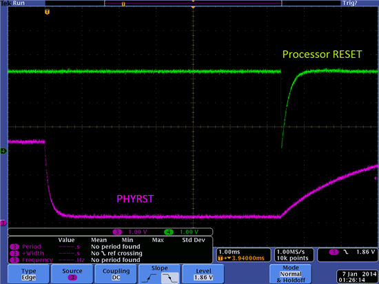
    Then, I had an idea to EXTEND PHYRST so it lasts longer than restart pulse: I added RC to PHYRST (GPIO63-100 Ohm-PHYRST-1.0 uF to GND) with tau about 620 us. The 100 Ohms is essential because there is R57 2.21K pull up resistor to 3.3V on this line, so R should be sufficiently low to create logic zero.

    In firmware, I configured GPIO63 as output, created a zero level on GPIO63, waited 4 ms, which brings PHYRST low, then enabled WDT, which resets processor, and it worked.

    Below are modifications of Concerto card: solder 0603 100 Ohm resistor between pins J9.6-J13.6, solder 0603 1.0 uF 10% capacitor between pin J9.6 and the closest pad of C41, which happens to be a ground.

    Signals on RC-modified Concerto Card:

    Below are new initialization and reboot functions:

    // Replace the old EthernetPinsSetup() function with this new one...
    //*****************************************************************************

    void EthernetPinsSetup(void)
    {
    // MII_TXD3
        GPIODirModeSet(  GPIO_PORTC_BASE, GPIO_PIN_4, GPIO_DIR_MODE_HW);
        GPIOPadConfigSet(GPIO_PORTC_BASE, GPIO_PIN_4, GPIO_PIN_TYPE_STD);
        GPIOPinConfigure(GPIO_PC4_MIITXD3);         // In file: gpio.C

    // MII_MDIO
        GPIODirModeSet(  GPIO_PORTE_BASE, GPIO_PIN_6, GPIO_DIR_MODE_HW);
        GPIOPadConfigSet(GPIO_PORTE_BASE, GPIO_PIN_6, GPIO_PIN_TYPE_STD);
        GPIOPinConfigure(GPIO_PE6_MIIMDIO);

    // MII_RXD3
        GPIODirModeSet(GPIO_PORTF_BASE, GPIO_PIN_5, GPIO_DIR_MODE_HW);
        GPIOPadConfigSet(GPIO_PORTF_BASE, GPIO_PIN_5, GPIO_PIN_TYPE_STD);
        GPIOPinConfigure(GPIO_PF5_MIIRXD3);

    // MII_TXER , MII_RXDV , MII_RXD1 , MII_RXD2
        GPIODirModeSet(  GPIO_PORTG_BASE, GPIO_PIN_7|GPIO_PIN_3|GPIO_PIN_1|GPIO_PIN_0,GPIO_DIR_MODE_HW);
        GPIOPadConfigSet(GPIO_PORTG_BASE, GPIO_PIN_7|GPIO_PIN_3|GPIO_PIN_1|GPIO_PIN_0, GPIO_PIN_TYPE_STD);
        GPIOPinConfigure(GPIO_PG0_MIIRXD2);
        GPIOPinConfigure(GPIO_PG1_MIIRXD1);
        GPIOPinConfigure(GPIO_PG3_MIIRXDV);
        GPIOPinConfigure(GPIO_PG7_MIITXER);

    // MII_TXCK , MII_TXEN , MII_TXD0 , MII_TXD1 , MII_TXD2 , MII_RXD0
        GPIODirModeSet(  GPIO_PORTH_BASE, GPIO_PIN_7|GPIO_PIN_6|GPIO_PIN_5|GPIO_PIN_4|GPIO_PIN_3|GPIO_PIN_1, GPIO_DIR_MODE_HW);
        GPIOPadConfigSet(GPIO_PORTH_BASE, GPIO_PIN_7|GPIO_PIN_6|GPIO_PIN_5|GPIO_PIN_4|GPIO_PIN_3|GPIO_PIN_1, GPIO_PIN_TYPE_STD);
        GPIOPinConfigure(GPIO_PH1_MIIRXD0);
        GPIOPinConfigure(GPIO_PH3_MIITXD2);
        GPIOPinConfigure(GPIO_PH4_MIITXD1);
        GPIOPinConfigure(GPIO_PH5_MIITXD0);
        GPIOPinConfigure(GPIO_PH6_MIITXEN);
        GPIOPinConfigure(GPIO_PH7_MIITXCK);

     // need to reset PHY because GPIO43 (BOOT defining PIN) is connected to PHY and prevents restart of silicon 1 // processor giving pulses 1.2 ms UNLESS PHY chip is in reset
        GPIOPinTypeGPIOOutput(GPIO_PORTJ_BASE, GPIO_PIN_7); //set as output: MII_PHYRSTn is simultaneously GPIO_63,
        GPIOPinWrite(GPIO_PORTJ_BASE, GPIO_BIT_7, M3_GPIOSET);   //write 1 to MII_PHYRSTn (GPIO_BIT_7) to release PHY chip

    // MII_PHYRSTn , MII_PHYINTRn , MII_CRS , MII_COL , MII_MDC , MII_RXCK , MII_RXER
        GPIODirModeSet(  GPIO_PORTJ_BASE, GPIO_PIN_6|GPIO_PIN_5|GPIO_PIN_4|GPIO_PIN_3|GPIO_PIN_2|GPIO_PIN_0, GPIO_DIR_MODE_HW);
        GPIOPadConfigSet(GPIO_PORTJ_BASE, GPIO_PIN_6|GPIO_PIN_5|GPIO_PIN_4|GPIO_PIN_3|GPIO_PIN_2|GPIO_PIN_0, GPIO_PIN_TYPE_STD);

    //test        GPIOPinWrite(GPIO_PORTJ_BASE, Bit_7, M3_GPIOCLR); //write 0 to MII_PHYRSTn (GPIO_BIT_7) reset PHY chip
    //test        GPIOPinWrite(GPIO_PORTJ_BASE, Bit_7, M3_GPIOSET); //write 1 to MII_PHYRSTn (GPIO_BIT_7) release PHY chip
       GPIOPinConfigure(GPIO_PJ0_MIIRXER);
       GPIOPinConfigure(GPIO_PJ2_MIIRXCK);
       GPIOPinConfigure(GPIO_PJ3_MIIMDC);
       GPIOPinConfigure(GPIO_PJ4_MIICOL);
       GPIOPinConfigure(GPIO_PJ5_MIICRS);
       GPIOPinConfigure(GPIO_PJ6_MIIPHYINTRn);
    //    GPIOPinConfigure(GPIO_PJ7_MIIPHYRSTn); // now it is an output
    }

    //*****************************************************************************
    void Reboot( void )

    {
        telnet_shutdown(); // Post telnet shutdown request to ISR
        cputs( "\r\nRestarting...\r\n" );
        GPIOPinWrite(GPIO_PORTJ_BASE, Bit_7, M3_GPIOCLR); //write "0" to MII_PHYRSTn (GPIO_BIT_7): reset PHY chip
        DELAY_US( 4000 ); // Allow 4 ms for ISR to service telnet shutdown request; and PHYRST line (after RC) acquire zero level
    // Enable the watchdog timer if it's not running already
    // if ( ! WatchdogRunning( WATCHDOG0_BASE ) )
    // {
            SysCtlPeripheralEnable( SYSCTL_PERIPH_WDOG0 );
    // }
        WatchdogUnlock( WATCHDOG0_BASE ); // Unlock writes to watchdog configuration.
        WatchdogResetEnable( WATCHDOG0_BASE ); // Enable reset generation from the watchdog timer.
        WatchdogReloadSet( WATCHDOG0_BASE, 0 ); // Set the period of the watchdog timer to 0 to get immediate results
        WatchdogEnable( WATCHDOG0_BASE ); // Enable the watchdog timer, allowing the reboot
    }


  • Igor,

    thanks for the update. Also there is another nice feature added on F28M35x REVA devices where user would be able to choose alternate boot mode pins if the factory chosen default ones doesn't fit the design. The details of this are yet to be added to the TRM or Datasheet but below is the essential.

    This is possible on F28M35x REVA/REVB Silicon by programming certain locations in user OTP.

    Location in OTP to program is 0x680824 . This would be a 32-bit location with below format - be careful while experimenting with this because this is OTP and it has ECC, which is in OTP as well. Program it only when you have finalized the IOs and know for sure what you need to program. You cannot change it once programmed.

    bmode_pin1 = bit0 - bit7  /*if you want to choose GPIO10 as bmode_pin1, then you need to program 0x0B (11 decimal) here, in other words, if you want to choose GPIOx you need to program GPIOx+1*/

    bmode_pin2 = bit8 - bit15 /*if you want to choose GPIO20 as bmode_pin2, then you need to program 0x15 (21 decimal) here, in other words, if you want to choose GPIOx you need to program GPIOx+1*/ 

    bmode_pin3 = bit16 - bit23 /*if you want to choose GPIO0 as bmode_pin3, then you need to program 0x01 (1 decimal) here, in other words, if you want to choose GPIOx you need to program GPIOx+1*/

     bmode_pin4 = bit24 - bit31 /*if you want to choose GPIO2 as bmode_pin4, then you need to program 0x03 (3 decimal) here, in other words, if you want to choose GPIOx you need to program GPIOx+1*/

    Even better - a TRICK, if you want to always boot-to-flash and you don't want to use four boot mode GPIO, you can program the same gpio pin value for each boot mode pin in the OTP word and have the pin pulled HIGH. Boot ROM will end up booting to flash, since it will read the same pin status for each boot mode pin, but please use it with caution.

    Now, the exceptions :-

    1.> you cannot choose below GPIO to be a boot mode GPIO.

    GPIO64, GPIO 65, GPIO66, GPIO67, GPIO39, GPIO44

    2.> chosen GPIO pins should be between GPIO0 and GPIO71. If any illegal value is found for any boot mode pin, then bootROM defaults to the factory selected boot mode pin respectively.

    Hope it helps. let us know if you have any questions.

    Best Regards

    Santosh

  • Thanks, Santosh.

    I have a chip with: SYSCTL_DID0 = 0x20400001, SYSCTL_DID1 = 0x1154804C, which should be "silicon A", correct?

    As I understood, silicon rev A (or rev B, has anybody seen it yet?) checks OTP address 0x680824 during M-boot.

    If this address has not been programmed, it boots the "old way" looking at: GPIO 34, 35, 47, 43 = bmode_pin1, 2, 3, 4.

    Q: I cannot read this particular address via emulator, it shows: --------  is it expected (see dump)? 

    I actually thought it should be 0xFFFFFFFF.

    If this address was programmed (and only then), it will look at the new pins, is it correct?

    Suppose we want to use OTP, but for a test exercise we make it exactly as old way, then:

    bmode_pin1 = GPIO_34+1 = 35D = 0x23

    bmode_pin2 = GPIO_35+1 = 36D = 0x24

    bmode_pin3 = GPIO_47+1 = 48D = 0x30

    bmode_pin4 = GPIO_43+1 = 44D = 0x2C

    so at address 0x680824 should be programmed 0x2C302423. Please confirm.


    Q: What is BOOT start address in OTP when bmode_pins are 0x6 (as they were in this case)?

    Q: If booting from OTP (bmode_pins are 0x6), user must program its own boot loader (rather short) there, correct?

    Dump, the fields marked as FFFFFFFF are described in TRM,

    the BOOT_PIN_SELECT address is marked as --------

    0x680600 60082007 0000F8BD D1042801 F2474911 6008001C F8BDE007 28020000 490DD103
    0x680620 0020F247 480C6008 6008490C 68004806 005EF36F D1F92800 68004802 B002B280
    0x680640 46C04770 50009D3C 50009D10 50009D0C 50009D30 50009D34 80000001 50009D08
    0x680660 4809B508 48099000 28066800 4908D10B F4406808 60083080 99004806 49064788
    0x680680 60084806 BD08E7FE 0100707D 20004534 20004000 0068082C E000ED0C 05FA0004
    0x6806A0 68004801 46C04770 00680810 68004801 46C04770 00680814 FFFFFFFF FFFFFFFF
    0x6806C0 FFFFFFFF FFFFFFFF FFFFFFFF FFFFFFFF FFFFFFFF FFFFFFFF FFFFFFFF FFFFFFFF
    0x6806E0 FFFFFFFF FFFFFFFF FFFFFFFF FFFFFFFF FFFFFFFF FFFFFFFF FFFFFFFF FFFFFFFF
    0x680700 FFFFFFFF FFFFFFFF FFFFFFFF FFFFFFFF FFFFFFFF FFFFFFFF FFFFFFFF FFFFFFFF
    0x680720 FFFFFFFF FFFFFFFF FFFFFFFF FFFFFFFF FFFFFFFF FFFFFFFF FFFFFFFF FFFFFFFF
    0x680740 FFFFFFFF FFFFFFFF FFFFFFFF FFFFFFFF FFFFFFFF FFFFFFFF FFFFFFFF FFFFFFFF
    0x680760 FFFFFFFF FFFFFFFF FFFFFFFF FFFFFFFF FFFFFFFF FFFFFFFF FFFFFFFF FFFFFFFF
    0x680780 FFFFFFFF FFFFFFFF FFFFFFFF FFFFFFFF FFFFFFFF FFFFFFFF FFFFFFFF FFFFFFFF
    0x6807A0 FFFFFFFF FFFFFFFF FFFFFFFF FFFFFFFF FFFFFFFF FFFFFFFF FFFFFFFF FFFFFFFF
    0x6807C0 FFFFFFFF FFFFFFFF FFFFFFFF FFFFFFFF FFFFFFFF FFFFFFFF FFFFFFFF FFFFFFFF
    0x6807E0 FFFFFFFF FFFFFFFF FFFFFFFF FFFFFFFF FFFFFFFF FFFFFFFF FFFFFFFF FFFFFFFF
    0x680800 FFFFFFFF -------- -------- FFFFFFFF FFFFFFFF FFFFFFFF -------- --------
    0x680820 -------- -------- -------- -------- -------- -------- -------- --------
    0x680840 -------- -------- -------- -------- -------- -------- -------- --------

  • Igor

    Igor Kordunsky said:
    I have a chip with: SYSCTL_DID0 = 0x20400001, SYSCTL_DID1 = 0x1154804C, which should be "silicon A", correct?

    YES.

    Igor Kordunsky said:

    As I understood, silicon rev A (or rev B, has anybody seen it yet?) checks OTP address 0x680824 during M-boot.

    If this address has not been programmed, it boots the "old way" looking at: GPIO 34, 35, 47, 43 = bmode_pin1, 2, 3, 4.

    Q: I cannot read this particular address via emulator, it shows: --------  is it expected (see dump)? 

    I actually thought it should be 0xFFFFFFFF.

    Hmm, this is probably because the GEL files don't define this memory regions. Either modify the GEL Memory Map or pull the value in the Expressions/watch window - *(volatile unsigned long *)address

    Igor Kordunsky said:

    If this address was programmed (and only then), it will look at the new pins, is it correct?

    Suppose we want to use OTP, but for a test exercise we make it exactly as old way, then:

    bmode_pin1 = GPIO_34+1 = 35D = 0x23

    bmode_pin2 = GPIO_35+1 = 36D = 0x24

    bmode_pin3 = GPIO_47+1 = 48D = 0x30

    bmode_pin4 = GPIO_43+1 = 44D = 0x2C

    so at address 0x680824 should be programmed 0x2C302423. Please confirm.

    yes that would be right.

    Igor Kordunsky said:

    Q: What is BOOT start address in OTP when bmode_pins are 0x6 (as they were in this case)?

    Q: If booting from OTP (bmode_pins are 0x6), user must program its own boot loader (rather short) there, correct?

    When boot-to-OTP is selected, bootROM branches to user OTP location 0x0068082C (again to view this memory in CCS you would need to add the zone to the GEL memory map).

    Yes, boot-to-otp feature is added for users to have a small loader and since this is one time programmable memory it is more useful for use cases which needs to support FW upgrade solutions.


    Hope this helps.


    Best Regards

    Santosh


  • Santosh,

    THE MOST IMPORTANT QUESTION: how to program OTHER ADDRESSES in OTP, if CCS (v5.5.077) "On-Chip Flash" window has only 4 fields available: OTPSELCLOCK, Z2_FLASH_START_ADDRESS, EMACID[31:0], EMACID[63:32]?

    without modifying GEL the CCS gives errors:

    The *(volatile unsigned long *)0x680824 gives error: Error line 1: unexpected token: long

    The *(long *)0x680824 gives error: Memory map prevented reading 0x00680824.   

    Modified GEL allows to see that area.

    I added continues area of 0x800 long for memory and 0x100 for ECC,but not sure it is correct.

    Q1: Please tell where OTP  ends, actually?:

    GEL_MapAddStr(0x680800,   0, 0x00800,   "R",   0);  /* OTP BANK 1 Application area*/

    Q2: if I write to OTP start location 0x0068082C a jump to bootROM "FLASH" branch, would it be equal to the behavior of Silicon rev 0?

    Q3: If Q2 answer is true, what is the jump address of bootROM "FLASH" branch?

    Original GEL:

        GEL_MapAddStr(0x0,        0, 0x10000, "R",    0);  /* M3 BOOT ROM                */
        GEL_MapAddStr(0x200000,   0, 0x80000, "R",    0);  /* FLASH BANK 1               */
        GEL_MapAddStr(0x600000,   0, 0x10000, "R|AS2",0);  /* FLASH BANK 1 ECC Bits      */
        GEL_MapAddStr(0x680000,   0, 0x00800, "R",    0);  /* OTP BANK 1                 */
        GEL_MapAddStr(0x680800,   0, 0x00004, "R",    0);  /* OTP BANK 1 Application 1   */
        GEL_MapAddStr(0x68080C,   0, 0x0000C, "R",    0);  /* OTP BANK 1 Application 2   */
        GEL_MapAddStr(0x700000,   0, 0x00100, "R|AS2",0);  /* OTP BANK 1 ECC Bits        */
        GEL_MapAddStr(0x700100,   0, 0x00003, "R|AS2",0);  /* OTP BANK 1 Applic ECC Bits */
        GEL_MapAddStr(0x1000000,  0, 0x10000, "R",    0);  /* M3 BOOT ROM (Dual Mapped)  */
        GEL_MapAddStr(0x4000000,  0, 0x4000000,"R",   0);  /* uCRC (Mirror 1 Space)      */


    Modified GEL (MODIFIED fields)

        GEL_MapAddStr(0x0,        0, 0x10000,   "R",   0);  /* M3 BOOT ROM               */
        GEL_MapAddStr(0x200000,   0, 0x80000,   "R",   0);  /* FLASH BANK 1              */
        GEL_MapAddStr(0x600000,   0, 0x10000,  "R|AS2",0);  /* FLASH BANK 1 ECC Bits     */
        GEL_MapAddStr(0x680000,   0, 0x00800,   "R",   0);  /* OTP BANK 1                */
        GEL_MapAddStr(0x680800,   0, 0x00800,   "R",   0);  /* OTP BANK 1 Application area*/
    /*  GEL_MapAddStr(0x68080C,   0, 0x0000C,   "R",   0);  /* OTP BANK 1 Application 2  */
        GEL_MapAddStr(0x700000,   0, 0x00100,  "R|AS2",0);  /* OTP BANK 1 ECC Bits       */
        GEL_MapAddStr(0x700100,   0, 0x00100,  "R|AS2",0);  /* OTP BANK 1 Applic ECC Bits*/
        GEL_MapAddStr(0x1000000,  0, 0x10000,   "R",   0);  /* M3 BOOT ROM (Dual Mapped) */
        GEL_MapAddStr(0x4000000,  0, 0x4000000, "R",   0);  /* uCRC (Mirror 1 Space)     */

  • Igor,

    Igor Kordunsky said:
    THE MOST IMPORTANT QUESTION: how to program OTHER ADDRESSES in OTP, if CCS (v5.5.077) "On-Chip Flash" window has only 4 fields available: OTPSELCLOCK, Z2_FLASH_START_ADDRESS, EMACID[31:0], EMACID[63:32]?

    for the above, I believe the team is looking into adding those new user OTP fields to the plugin, but until then you can use a user defined section (using #PRAGMA) in your project and link some constant data to the needed OTP sections/addresses. Remember this is OTP is is one time programable only, ecc for the OTP memory is also in OTP so that means entire 64 bits of OTP data are to be programmed at one go. 

    Igor Kordunsky said:

    Q2: if I write to OTP start location 0x0068082C a jump to bootROM "FLASH" branch, would it be equal to the behavior of Silicon rev 0?

    Q3: If Q2 answer is true, what is the jump address of bootROM "FLASH" branch?

    for Q2, the answer is yes. Boot-to-OTP is supported on TMS version of Si. Yo ucan also check the OTP version in Si, if the OTP version is atleast 0x03 then the device has boot-to-otp support. OTP version can be found at location 0x68047C. If there is no boot-otootp support on Si then boot mode 6 boots to flash.

    for Q3, the answer is in the TRM boot ROM chapter section 6.5.6.1, so in OTP at location 0x0068082C you would need to add a 'branch to 0x200031', if you are using the default boot-to-flash entry point of 0x200030.

    User OTP usage distribution on REV0 and REVA is as below:- TRM and datasheet updates for this are pending.

    F28M35x REV0

    User OTP location Address

    REV0 Usage

    Notes

    0x680800

    OTP Security LOCK

    ECC is shared for these, so these two must be programmed at once

    0x680804

    EMAC MAC ID 0

    0x680808

    EMAC MAC ID 1

    ECC is shared for these, so these two must be programmed at once

    0x68080C

    Z2 FLASH ENTRY POINT


    F28M35x REVA 

    User OTP location Address

    REVA Usage

    Notes

    0x680800

    OTP Security LOCK

    Combined ECC

    0x680804

    Reserved

    0x680808

    Reserved

    Combined ECC

    0x68080C

    Z2 FLASH ENTRY POINT

    0x680810

    EMAC_REG0_ADDR

    Combined ECC

    0x680814

    EMAC_REG1_ADDR

    0x680818

    Reserved

    Combined ECC

    0x68081C

    MAIN_OSC_CLK_FREQ

    0x680820

    Reserved

    Combined ECC

    0x680824

    Alternate Boot mode Pin Config

    0x680828

    Reserved

    Combined ECC

    0x68082C

    OTP_ENTRY_POINT


    Hope this helps

    Best Regards

    Santosh

  • oh, user usable OTP ends at 0x680FFF. 

  • Thank you, Santosh!

    To follow your guidance, I created an assembler file, and few entries in link file: new MEMORY line, and a new SECTION line:

    ;//====================================

    ;// This code for OTP memory of Silicon A, which has an option "Boot from OTP" when boot-pins = 0x6
    ;// Silicon 0 when boot pins = 0x6 does not have this and instead boots from FLASH (boot-pins = 0x7)
    ;// If place at OTP boot start address "branch to Boot from FLASH", it will mimic rev 0 behavior
        ; Thumb instruction set
        .thumb

        ; Code section
        .sect ".OTPboot"    ; 0x0068082C OTP boot start address,
    ;// in link file:    create section in SECTIONS{     .OTPboot      :   >  OTP_ENTRY_POINT} ;, where
    ;// OTP_ENTRY_POINT is in MEMORY{     OTP_ENTRY_POINT : origin = 0x0068082C, length = 0x07D4}   // OTP BANK 1 Boot from OTP code

    OTP_boot:
        .asmfunc
        LDR     r0, bootFLASH                         ; load address  0x200031 into R0
        BX.W    r0                                    ; branch to 0x200030
        .endasmfunc
        ; Fields that can be accessed with LDR
    bootFLASH .field  0x00200031, 32                  ; Address of BootROM to FLASH
    ;//    .word  0x00200031  ;Flash_boot_adr

    ;//====================================

    It compiles, but I do not see any space taken at address in the map file:

             name            origin    length      used     unused   attr    fill
    ----------------------  --------  ---------  --------  --------  ----  --------
      OTP_ENTRY_POINT       0068082c   000007d4  00000000  000007d4  RWIX

    Question 1: Why this assembler function does not reserve any space, what is wrong?

    Question 2: How to generate ECC, manually? or flash loader will do it?

    You mentioned that "Remember this is OTP is is one time programmable only, ecc for the OTP memory is also in OTP so that means entire 64 bits of OTP data are to be programmed at one go."

    Question 3: I understood this as: A 32 bit word in OTP main address and 32bit word in OTP ECC need to be programed in one function call or both fields must be defined in an .out (or .hex, or .ehx) file. Please confirm.

     Of cause we cannot re-write already programmed address in OTP, but yet another.

    Question 4: is it possible to program one location, and later another location, and so on, or
    an entire OTP must be programmed "at once"?


  • Igor,

    Igor Kordunsky said:
    Question 1: Why this assembler function does not reserve any space, what is wrong?

    regarding above, I gues the linker is removing the sections that are not referenced. try to use --retain=_OTP_boot

    Igor Kordunsky said:
    Question 2: How to generate ECC, manually? or flash loader will do it?

    Nope, ECC can be chosen to be auto-generated and auto-programmed when using plugin (that's the default option). Don't worry about it.

    Igor Kordunsky said:

    You mentioned that "Remember this is OTP is is one time programmable only, ecc for the OTP memory is also in OTP so that means entire 64 bits of OTP data are to be programmed at one go."

    Question 3: I understood this as: A 32 bit word in OTP main address and 32bit word in OTP ECC need to be programed in one function call or both fields must be defined in an .out (or .hex, or .ehx) file. Please confirm.

    I mean, for each 64 bits of DATA the ECC is some X bits (refer to Flash API guide). In other words for ex: you cannot chose to program location 0x680810 now and 0x680814 later on because both these locations share a common ECC code. Whenever you program 0x680810 you will want to make sure you know what to program at 0x680814 as well. That's the reason I showed the locations which have combined ECC code in the above post.

    Igor Kordunsky said:

    Question 4: is it possible to program one location, and later another location, and so on, or
    an entire OTP must be programmed "at once"?

    as long as the locations doesn't share common ECC code you will be fine. This is shown in the above table, for reserved locations you can leave the value at 0xFFFFFFFF.


    Hope this helps.


    Best Regards

    Santosh

  • I'm attempting to force booting from flash on a product that is already using all of the default boot pins for other purposes. We do, however, have GPIO32 pulled high. I've been trying to program the boot pin reassignment OTP memory at 0x00680824 to 0x21212121 but I can't seem to write to it. Things I've done:

    • Updated the GEL to include the memory location as R|W:

      GEL_MapAddStr(0x68080C,      0, 0x00020,    "R|W",   0);        /* OTP BANK 1 Application 2            */

      This allows me to read that location in memory using CCS memory browser, but I can't write to it. No matter what I set it to, reading back from it always returns 0xffffffff.
    • Generated a binary that forces a variable to that location in memory, and flashed it:

      #pragma RETAIN(boot_otp)
      #pragma LOCATION(boot_otp, 0x00680824);
      const unsigned long boot_otp = 0x21212121;

      I also added the following to my linker *.cmd file:

      MEMORY

      {
          ......
          OTP (RW) : origin = 0x00680824, length = 0x04
      }

      This looks like it should work (everything is mapped properly in the *.out file), but when I flash it and check the value of boot_otp, it still shows 0xffffffff.

    Am I missing something? Is the OTP protected somehow and I need to disable the protection before flashing?

    Regards,
    Matt

  • Matt,

    yes, this is OTP region so you wont be able to program it from memory browser on CCS. The way of COFF file load you are using is the proper approach. Code looks good that should work, have you updated your device XMLs and are using latest flash plug-in available for device?


    Best Regards

    Santosh


  • Santosh Athuru said:
    Code looks good that should work, have you updated your device XMLs and are using latest flash plug-in available for device?

    I don't know. How can I tell? I'm using a version of CCS and controlSUITE that I downloaded only a few months ago.

    Is it possible that somehow I've accidentally programmed the location to 0xFFFFFFFF and my subsequent attempts are failing because it is OTP? Is there any way to tell if the OTP has been programmed?

  • Matthew,

    yes it is possible that you might have written 0xFFFFFFFF, you can figure if you have programmed it please look at the OTP ECC bits locations. This must be documented in the data sheet memory map, for every 64 bits there will be an 8 bit ECC so you will have to look at the ECC bits address locations in the memory corresponding to those addresses in OTP.

    If you install a fresh copy of CCSv5 then you should get the latest XMLs an flash plug-in the support to program user OTP is added couple of months back may be you don't have it. I'm trying to find if there is any versioning with the XMLS or plug-in to say which one you have, hopefully I will get to this tomorrow.


    Best Regards

    Santosh

  • Santosh Athuru said:

    yes it is possible that you might have written 0xFFFFFFFF, you can figure if you have programmed it please look at the OTP ECC bits locations. This must be documented in the data sheet memory map, for every 64 bits there will be an 8 bit ECC so you will have to look at the ECC bits address locations in the memory corresponding to those addresses in OTP.

    I've looked at the 6 bytes starting at 0x00700100, which are supposedly the ECC bits for user OTP 0x00680800 - 0x0068082F. They are 0xFF 0xFF 0xFF 0xFF 0xFF 0xFF. I don't know how the ECC bits are calculated, so I don't know if that means I have or haven't programmed the OTP already. Is it a simple parity bit?

    Santosh Athuru said:

    If you install a fresh copy of CCSv5 then you should get the latest XMLs an flash plug-in the support to program user OTP is added couple of months back may be you don't have it. I'm trying to find if there is any versioning with the XMLS or plug-in to say which one you have, hopefully I will get to this tomorrow.

    I can confirm that my copy of CCS is the latest available on the TI site (5.5.0.00077). I also have the latest copy of Uniflash. Looking at the XML files with each of those, they appear to be for Rev0 and RevA silicon. One disconcerting thing I did pick up is this:

    <Otp Type="Otp" StartAddress="0x00680800" Length="0x00000018">
    	<Correction Type="OtpEcc" StartAddress="0x00700100" Length="0x00000003"/>
    </Otp>

    Is the problem that the XML file stops the OTP at 0x00680817? Can I safely modify the XML file? Is there a later XML file that you can link me to that will allow me to program the OTP?

  • Matthew,

    thanks for checking and sorry for the confusion, I just got the confirmation from flash owner that the XML update to program the user OTP beyond 0x680817 is yet to be released for F28M35x. He is going to provide us with the updated XML, I'm checking with him if XML file modification is all that is needed?


    Best Regards

    Santosh


  • Matthew,

    try the attached XML, this is still work under progress and you would see an error message at the end but you can ignore it (Vamsi tried this and saw it is programming the userOTP). He is working to clean it up but if this works meanwhile for you then you should be able to get the clean one in the next official update.


    5228.F28M35x.M3.xml
    <?xml version="1.0" encoding="UTF-8"?>
    <Device  AsicId="0x771589" DeviceId="0x771589" Library="f021_m3_le.nfl" CoreType="M3_LittleEndian" useDAP="false" Revision="1" >
        <Revisions>
            <Revision RevisionNumber="0"> Initial Revision </Revision>
            <Revision RevisionNumber="1"> Updated to new schema </Revision>
        </Revisions>
        <Part Name="F28M35xm">
            <MinorRevision RevisionNumber="0" Description="F28M35xm Rev 0"/>
    		<MinorRevision RevisionNumber="1" Description="F28M35xm Rev A"/>
            <RegisterId Address="0x680410" Value="0x6" Mask="0x0007" Comment="MNCF register Bits 0to2 value is 0x6 for 256KB"/>
            <Parameters>
                <MemoryMap>
                    <Flash>
                        <ProgramFlash    StartAddress="0x00200000" EndAddress="0x0027FFFF" CorrectionStartAddress="0x00600000" CorrectionEndAddress="0x0060FFFF"/>
                        <ProgramFlashOtp StartAddress="0x00680800" EndAddress="0x00680FFF" CorrectionStartAddress="0x00700100" CorrectionEndAddress="0x007001FF"/>
                        <Bank Number="0" Type="Program" ControlRegister="0x400FA000"
                            StartAddress="0x00200000" EndAddress="0x0027FFFF"
                            CorrectionStartAddress="0x00600000" CorrectionEndAddress="0x0060FFFF">
                            <Sector Number="0" Type="Flash" StartAddress="0x00200000" Length="0x00004000">
                                <Correction Type="FlashEcc" StartAddress="0x00600000" Length="0x00000800"/>
                            </Sector>
                            <Sector Number="1" Type="Flash" StartAddress="0x00204000" Length="0x00004000">
                                <Correction Type="FlashEcc" StartAddress="0x00600800" Length="0x00000800"/>
                            </Sector>
                            <Sector Number="2" Type="Flash" StartAddress="0x00208000" Length="0x00004000">
                                <Correction Type="FlashEcc" StartAddress="0x00601000" Length="0x00000800"/>
                            </Sector>
                            <Sector Number="3" Type="Flash" StartAddress="0x0020C000" Length="0x00004000">
                                <Correction Type="FlashEcc" StartAddress="0x00601800" Length="0x00000800"/>
                            </Sector>
                            <Sector Number="4" Type="Flash" StartAddress="0x00210000" Length="0x00010000">
                                <Correction Type="FlashEcc" StartAddress="0x00602000" Length="0x00002000"/>
                            </Sector>
                            <Sector Number="9" Type="Flash" StartAddress="0x00260000" Length="0x00010000">
                                <Correction Type="FlashEcc" StartAddress="0x0060C000" Length="0x00002000"/>
                            </Sector>
                            <Sector Number="10" Type="Flash" StartAddress="0x00270000" Length="0x00004000">
                                 <Correction Type="FlashEcc" StartAddress="0x0060E000" Length="0x00000800"/>
                            </Sector>
                            <Sector Number="11" Type="Flash" StartAddress="0x00274000" Length="0x00004000">
                                 <Correction Type="FlashEcc" StartAddress="0x0060E800" Length="0x00000800"/>
                            </Sector>
                            <Sector Number="12" Type="Flash" StartAddress="0x00278000" Length="0x00004000">
                                 <Correction Type="FlashEcc" StartAddress="0x0060F000" Length="0x00000800"/>
                            </Sector>
                            <Sector Number="13" Type="Flash" StartAddress="0x0027C000" Length="0x00004000">
                                 <Correction Type="FlashEcc" StartAddress="0x0060F800" Length="0x00000800"/>
                            </Sector>
                            <Otp Type="Otp" StartAddress="0x00680800" Length="0x00001000">
                                <Correction Type="OtpEcc" StartAddress="0x00700100" Length="0x00000200"/>
                            </Otp>
                        </Bank>
                        </Flash>
                </MemoryMap>
            </Parameters>
        </Part>
        <DefaultPart Name="F28M35xh">
            <MinorRevision RevisionNumber="0" Description="F28M35xh Rev0"/>
    		<MinorRevision RevisionNumber="1" Description="F28M35xh RevA"/>
            <Parameters>
                <MemoryMap>
                    <Flash>
                        <ProgramFlash    StartAddress="0x00200000" EndAddress="0x0027FFFF" CorrectionStartAddress="0x00600000" CorrectionEndAddress="0x0060FFFF"/>
                        <ProgramFlashOtp StartAddress="0x00680800" EndAddress="0x00680FFF" CorrectionStartAddress="0x00700100" CorrectionEndAddress="0x007001FF"/>
                        <Bank Number="0" Type="Program" ControlRegister="0x400FA000"
                            StartAddress="0x00200000" EndAddress="0x0027FFFF"
                            CorrectionStartAddress="0x00600000" CorrectionEndAddress="0x0060FFFF">
                            <Sector Number="0" Type="Flash" StartAddress="0x00200000" Length="0x00004000">
                                <Correction Type="FlashEcc" StartAddress="0x00600000" Length="0x00000800"/>
                            </Sector>
                            <Sector Number="1" Type="Flash" StartAddress="0x00204000" Length="0x00004000">
                                <Correction Type="FlashEcc" StartAddress="0x00600800" Length="0x00000800"/>
                            </Sector>
                            <Sector Number="2" Type="Flash" StartAddress="0x00208000" Length="0x00004000">
                                <Correction Type="FlashEcc" StartAddress="0x00601000" Length="0x00000800"/>
                            </Sector>
                            <Sector Number="3" Type="Flash" StartAddress="0x0020C000" Length="0x00004000">
                                <Correction Type="FlashEcc" StartAddress="0x00601800" Length="0x00000800"/>
                            </Sector>
                            <Sector Number="4" Type="Flash" StartAddress="0x00210000" Length="0x00010000">
                                <Correction Type="FlashEcc" StartAddress="0x00602000" Length="0x00002000"/>
                            </Sector>
                            <Sector Number="5" Type="Flash" StartAddress="0x00220000" Length="0x00010000">
                                <Correction Type="FlashEcc" StartAddress="0x00604000" Length="0x00002000"/>
                            </Sector>
                            <Sector Number="6" Type="Flash" StartAddress="0x00230000" Length="0x00010000">
                                <Correction Type="FlashEcc" StartAddress="0x00606000" Length="0x00002000"/>
                            </Sector>
                            <Sector Number="7" Type="Flash" StartAddress="0x00240000" Length="0x00010000">
                                <Correction Type="FlashEcc" StartAddress="0x00608000" Length="0x00002000"/>
                            </Sector>
                            <Sector Number="8" Type="Flash" StartAddress="0x00250000" Length="0x00010000">
                                <Correction Type="FlashEcc" StartAddress="0x0060A000" Length="0x00002000"/>
                            </Sector>
                            <Sector Number="9" Type="Flash" StartAddress="0x00260000" Length="0x00010000">
                                <Correction Type="FlashEcc" StartAddress="0x0060C000" Length="0x00002000"/>
                            </Sector>
                            <Sector Number="10" Type="Flash" StartAddress="0x00270000" Length="0x00004000">
                                 <Correction Type="FlashEcc" StartAddress="0x0060E000" Length="0x00000800"/>
                            </Sector>
                            <Sector Number="11" Type="Flash" StartAddress="0x00274000" Length="0x00004000">
                                 <Correction Type="FlashEcc" StartAddress="0x0060E800" Length="0x00000800"/>
                            </Sector>
                            <Sector Number="12" Type="Flash" StartAddress="0x00278000" Length="0x00004000">
                                 <Correction Type="FlashEcc" StartAddress="0x0060F000" Length="0x00000800"/>
                            </Sector>
                            <Sector Number="13" Type="Flash" StartAddress="0x0027C000" Length="0x00004000">
                                 <Correction Type="FlashEcc" StartAddress="0x0060F800" Length="0x00000800"/>
                            </Sector>
                            <Otp Type="Otp" StartAddress="0x00680800" Length="0x00001000">
                                <Correction Type="OtpEcc" StartAddress="0x00700100" Length="0x00000200"/>
                            </Otp>
                        </Bank>
                        </Flash>
                </MemoryMap>
            </Parameters>
        </DefaultPart>
        <CommonParameters>
            <Initialization>
                <InitRegisters Register="0x400FB980" Value="0xA5A5A5A5" Comment="allow writes to protected registers"/>            
                <InitRegisters Register="0x400FE100" Value="0x00000000" Comment="disable watchdog timer0 and watchdog timer 1"/>
                <InitRegisters Register="0x400FA600" Value="0x00000000" Comment="disable ecc"/>
                <InitRegisters Register="0x400FA000" Value="0x00000100" Comment="RWAIT=1"/>
                <InitRegisters Register="0x400FA040" Value="0x0000FFFF" Comment="force active mode for all banks"/>
                <InitRegisters Register="0x400FA300" Value="0x00000000" Comment="Disable cache and prefetch and this is default on powerup"/>
            </Initialization>
        </CommonParameters>
    </Device>
    

    please let us know your feedback.

    Best Regards

    Santosh


  • Worked perfectly, thanks!

    Cortex_M3_0: GEL Output: Memory Map Initialization Complete
    Cortex_M3_0: GEL Output: Watchdog Timers Enabled
    Cortex_M3_0: GEL Output: UARTs Enabled
    Cortex_M3_0: Writing Flash @ Address 0x00680824 of Length 0x00000004
    Cortex_M3_0: Erasing Flash Bank 0, Sector N
    Cortex_M3_0: Erasing Flash Bank 0, Sector M
    Cortex_M3_0: Erasing Flash Bank 0, Sector L
    Cortex_M3_0: Erasing Flash Bank 0, Sector K
    Cortex_M3_0: Erasing Flash Bank 0, Sector J
    Cortex_M3_0: Erasing Flash Bank 0, Sector I
    Cortex_M3_0: Erasing Flash Bank 0, Sector H
    Cortex_M3_0: Erasing Flash Bank 0, Sector G
    Cortex_M3_0: Erasing Flash Bank 0, Sector F
    Cortex_M3_0: Erasing Flash Bank 0, Sector E
    Cortex_M3_0: Erasing Flash Bank 0, Sector D
    Cortex_M3_0: Erasing Flash Bank 0, Sector C
    Cortex_M3_0: Erasing Flash Bank 0, Sector B
    Cortex_M3_0: Erasing Flash Bank 0, Sector A
    Cortex_M3_0: Data has been buffered at the beginning of the current data block for 64-bit aligned writes.
    Cortex_M3_0: Finish Writing Flash @ Address 0x00680824 of Length 0x00000004
    Cortex_M3_0: Writing buffered data @ Address 0x00680820 of Length 0x00000008
    Cortex_M3_0: Verifying Flash @ Address 0x00680820 of Length 0x00000008

  • Santosh,


    How do i perform the TRICK where I program OTP on a F28M36 so it always boots from flash independent of the boot pins?  Thank you so much for you help in advance.


  • Douglas,

    Unfortunately that feature is not available on F28M36x, it is available on F28M35x TMS Si only. 

    Best Regards

    Santosh

  • Hi Santosh,


    I have a Concerto controllerCARD with F28M36c2.  i removed the SW1 and R8, R9, R10, R11 in order to make the boot pins as no-connects on the controllerCARD.  I programmed the flash with a standalone flash blinky program.  During a power cycle, it boots very quickly from FLASH.  Is this the expected behavior?  Are the GPIO boot pins internal pull ups, so without anything connected to them, they automatically go to boot from flash?


  • Douiglas,

    pull ups should be disabled by reset, as per section 4.1.6.12 (page 371) of TRM. Can you cross check the GPIOPUR register values for the pins to confirm also check the voltage at the pin.

    also, any unsupported boot mode select value ends up with boot to flash as well, as shown in the boot mode selct table in the data sheet (the TRM boot mode selct table is not up-to-date). 

    Best Regards

    Santosh

  • Dear Santosh,

    I am stuck exactly with the same problem and reading this thread has been really useful in order to find a solution. Due to the fact that this is OTP, before proceeding I would like to confirm is the steps I will follow are correct:

    1) I am under CCSv6 (version 6.0.1.201406261800 on Linux)

    2) I am going to force the Boot to Master Subsystem Flash memory (mode 0111). This is, as documented in Table 3-18. Master Subsystem Boot Mode Selection appearing on pp. 39 for document  f28m35m52c.pdf:

    PF2_GPIO34: 0

    PF3_GPIO35: 1

    PG7_GPIO47: 1

    PG3_GPIO43: 1

    The question is to which bytes correspond each of the lines. At the same table it is said the following:

    PF2_GPIO34/BOOT_3

    PF3_GPIO35/BOOT_2

    PG7_GPIO47/BOOT_1

    PG3_GPIO43/BOOT_0

    Are they then corresponding to this order?:

    PF2_GPIO34/BOOT_3/bmode_pin4

    PF3_GPIO35/BOOT_2/bmode_pin3

    PG7_GPIO47/BOOT_1/bmode_pin2

    PG3_GPIO43/BOOT_0/bmode_pin1

    or the other way around?

    PF2_GPIO34/BOOT_3/bmode_pin1

    PF3_GPIO35/BOOT_2/bmode_pin2

    PG7_GPIO47/BOOT_1/bmode_pin3

    PG3_GPIO43/BOOT_0/bmode_pin4

    Using the first combination, the contents of the memory location will be 0x00680824: 0x23242424 and using the second option should be 0x24242423 (in both options I am using your proposed trick of just using one line (GPIO35) for forcing the 1 and GPIO34 is kept at 0)

    3) For programming the OTP I will use the code already given in this thread:

    /#pragma RETAIN(boot_otp)
    #pragma LOCATION(boot_otp, 0x00680824);
    const unsigned long boot_otp = 0x24242423; // <--  NOTE THIS VALUE DEPENDS ON YOUR ANSWER

    and the corresponding modifications at the .xml file (5228.F28M35x.M3.xml) post before to this thread.

    Thanks in advance,

    Pablo

  • Pablo Garcia said:

    PF2_GPIO34/BOOT_3/bmode_pin4

    PF3_GPIO35/BOOT_2/bmode_pin3

    PG7_GPIO47/BOOT_1/bmode_pin2

    PG3_GPIO43/BOOT_0/bmode_pin1

    above is correct.  and in OTP the bits should be organized as below. This is explained in post http://e2e.ti.com/support/microcontrollers/c2000/f/171/t/339389.aspx; 

    /* bmode_pin1 = bit0 - bit7 */
    /* bmode_pin2 = bit8 - bit15 */
    /* bmode_pin3 = bit16 - bit23 */
    /* bmode_pin4 = bit24 - bit31 */

    Best Regards

    Santosh Athuru