This thread has been locked.

If you have a related question, please click the "Ask a related question" button in the top right corner. The newly created question will be automatically linked to this question.

TMS320F28377D how to setup a trip zone event?

Other Parts Discussed in Thread: CONTROLSUITE, TMS320F28377D, DESIGNDRIVE

At the TMS320F28377D there exist in contrary to the Piccolos no dedicated trip zone inputs. In the manual the input x-bar is mentioned. Is the external trip no possible with all GPIO lines? Please give me a a small example code what I have to to stop EPWM1A by an external trip exent on a GPIO. The information in the datasheet is not detailed enough and there is no example in controlsuite. I can test it  on my TMDSCNCD28377D control card with the epwm_updown_aq_cpu01 example of the controlsuite!

  • Hi Dr. Stiebel,

    We definitely need to provide multiple examples of how to configure the X-BARs in ControlSUITE and make the documentation more clear.  

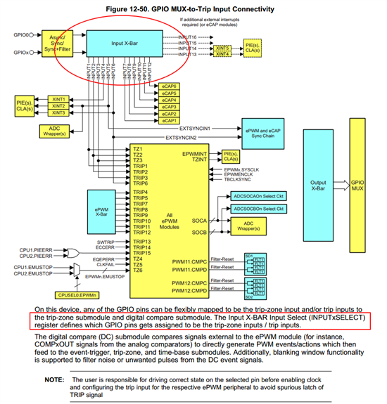
    In the meantime, here is a trace-through of the GPIO to the ePWM via the XBARs (all of this information is in the TRM, http://www.ti.com/lit/ug/spruhm8/spruhm8.pdf):

    The input X-bar can be configured to select any GPIO:

    These are configured by the INPUTxSELECT registers:

    Inputs 1,2,3, and 6 go directly into the ePWM DC:

    And inputs 1 through 6 go to the ePWM XBAR (not shown on fig 12-50):

    This can be configured as per figure 12-58 and table 12-14 with registers found in section 12.6. The outputs go to TRIP 4,5 and 7 through 12.

  • Hi Devin, I have a question concerning the TRIP1~12. So with TZSEL register we can select which TZ signal is to use by the ePWM module, but how to select which TRIP signal is used by the module? The TRIP and TZ signal should be the same in terms of stoping PWM output, is that right? Thank you!
  • All I have been able to do is generate three trip zone signals from external GPIO pins using TZ1-TZ3.  I need to be able to generate 7 external trips.  How can this be done?

    For instance I am able to use the following code:

    EALLOW;

    InputXbarRegs.INPUT1SELECT = 70;

    Edis

    EALLOW;

    EPwm1Regs.TZSEL.bit.CBC1 = 1;

    EPwm1Regs.TZCTL.bit.TZA = TZ_FORCE_LO;

    EPwm1Regs.TZCTL.bit.TZB = TZ_FORCE_LO;

    // Enable TZ interrupt

    EPwm1Regs.TZEINT.bit.CBC = 1;

    EDIS;

    But I cannot use:

    InputXbarRegs.INPUT4SELECT = 34;

    for input 4, 5, or 6 because they are connected to internal trips such as eQEP etc.

    and then of course I would use:

    EPwm1Regs.TZSEL.bit.CBC4 = 1;

    Then the problem is with EPwmxRegs.TZSEL.bit.CBCx is that CBC only allows has six bits for CBC (1-6).  So since 4-6 are taken by internals it looks like this controller only allows for three trips from GPIOs. 

    Please help me to understand how to get seven external trip signals.

    Thanks so much!

  • Hi Adam,

    You are correct in your understanding of how TZ1-6 work.  This is often the most direct route to tripping a PWM.  However, there are more options than just TZ1-TZ6. 

    Specifically, you should note that the INPUTXBAR INPUT1-6 can connect up to the EPWMXBAR.  The EPWMXBAR outputs TRIP4,5,7-12 which feed to all ePWM peripheral.  (see figure 13-56 of the current TRM - spruhm8d)

    These TRIPs can be fed into the Digital Compare submodule of the ePWM peripheral.  By editing DCTRIPSEL (and some other settings), you should be able to generate DCxEVTn.force events.  Note also that there is an option to OR a lot of TRIPs together and also options to do some filtering on the TRIPs.  (see figure 13-48 of the current TRM) 

    The DCxEVTn.force events go as inputs into the TZSEL registers which I think you already comprehend.

    I realize this is a bit more of a headache to get right, but the ability is there to do what you want.  There is also more functionality that can be gained when using the less direct path - the ability to asynchronously AND and OR inputs as you go through the chip.


    Thank you,
    Brett

  • Brett,

    Thank you for the response. I am still a little confused about this because aren't InputXBar Inputs 4-6 automatically connected to internal trips? So that still only allows me to connect Inputs 1-3 to external GPIO's as the trip source.

    How can I get 7 external GPIO's to the trips 4,5,7-12?

    Also, where in the manual is the section about OR ing inputs as this will also be important for me?

    Thanks,

    Adam
  • Hi Adam,

    Adam Stevens53 said:


    Thank you for the response. I am still a little confused about this because aren't InputXBar Inputs 4-6 automatically connected to internal trips? So that still only allows me to connect Inputs 1-3 to external GPIO's as the trip source.


    No.  The outputs of INPUTXBAR1-3 create the signals TZ1-3 (among other things).  Furthermore, internal events do generate TZ4-6 as you say.  However, the outputs of INPUTXBAR4-12 attach to other things in the system.  In particular INPUTXBAR1-6 can go into the PWMXBAR. Figure 7-6 in the current TRM may help clarify things.

    Adam Stevens53 said:


    How can I get 7 external GPIO's to the trips 4,5,7-12?


    As explained, you should definitely be able to get 6 GPIOs to trip PWMs (INPUTXBAR outputs 1-6).  I'd recommend using a comparator output, going through the PWMXBAR, to get a seventh.

    Adam Stevens53 said:


    Also, where in the manual is the section about OR ing inputs as this will also be important for me?


    Take a look at the figures I mentioned in the earlier post.


    Thank you,
    Brett

  • Hello Brett,

    I have gone through the documentation in quite a bit of detail and have made some good progress in understanding how this works.  However, have one major disconnect in understanding how the input to the compare module is set.  I have been using the HVDMC_Protection function in the DesignDrive IDDK example code as a reference.

    Table 13-13 of the technical reference manual shows what inputs go into each mux.  So in the IDDK example they use input 1 for each of these muxes: MUX0, MUX4, MUX2, MUX10, and MUX1; which corresponds to CMPSS1.CTRIPH, CMPSS3.CTRIPH, CMPSS2.CTRIPH, CMPSS6.CTRIPH, CMPSS1.CTRIPL respectively.

    The disconnect I have is how these CMPSS values are connect to the appropriate ADC or INPUTXBAR values.  For instance CMPSS1.CTRIPH should be connected to ADCA ch2, CMPSS3.CTRIPH should be connected to ADCB ch2, CMPSS2.CTRIPH should be connected to ADCA ch4, CMPSS6.CTRIPH should be connected to ADCC ch 2, and CMPSS1.CTRIPL is connected to INPUTXBAR1 which is set to GPIO 40.

    I cannot find in the code how the connection to the various CMPSS values is made to the respective ADC.  This is my main disconnect.

    Also, I do not understand why for the INPUTXBAR1 they did not use MUX1 input 2 instead of MUX1 input 1.

    Thanks so much for your help.

    -Adam

  • Hi Adam,

    Adam Stevens53 said:

    I cannot find in the code how the connection to the various CMPSS values is made to the respective ADC.  This is my main disconnect.


    The Comparator SubSystem doesn't really require the ADC to work in order to function.  The analog comparators merely share the same pins as the ADC inputs.  The analog comparators are set up in the cmpssConfig function.


    Adam Stevens53 said:

    Also, I do not understand why for the INPUTXBAR1 they did not use MUX1 input 2 instead of MUX1 input 1.


    I believe you are correct, and that this is an error in the code.  I will submit a bug so this gets looked at in a future software release.


    Hopefully this helps!


    Thank you,
    Brett

  • Adam Stevens53 said:

    I cannot find in the code how the connection to the various CMPSS values is made to the respective ADC.  This is my main disconnect

    Another thing to note is that the ADC is always connected to the CMPSS pin so there is no software to configure for this.

  • That's very interesting!

    We have the IDDK kit and have been going through the build steps. Build 2 says to increase the Vqtesting and Vdtesting variables in order to see what voltage gives a distorted current waveform and then set the variables pi_iqUmax and pi_idUmin to those voltages respectively. However we are getting trips immediately sometimes even before setting the RunMotor enable variable. But when we do run the motor and clear the trip flag then I change the Vqtesting value from .1 to .12 the motor trips. Something must not be set up right. I believe the ADC is set up properly as I can view the waveforms on the graph from the memory so it must be something with the comparator.

    Also, you said that the ADC is always connected to the CMPSS pin so how can I tell that ADC A4 is connected to Cmpss2 and and ADC C2 is connected to Cmpss6? Is there a table or something in the reference manual that shows these connections?

    Also, for the bug report I changed the input of  MUX1 to be 2 in order to set it to inputxbar something strange happens.  The motor trips but now the tripflag does not get set and EPwm1Regs.TZFLG.bit.OST remains at 0.  However when I reduce the Vqtesting voltage back and then clear the trip flag it begins to work again.  This makes me think that the ocp latch is tripping without triggering TRIP4.

  • Hi Adam,

    Comparator and ADC connections:
    The F2837xD datasheet is where you can find the details on pin descriptions and you will find your missing link there. 

    IDDK kit and its tripping:
    If it's okay with you, let's move the IDDK discussion to a new thread.  Just create a new post.


    Thank you,
    Brett

  • Adam,

    For the analog pin assignments, you can refer to the datasheet:

    Terminal Configurations and Functions -> Signal Descriptions Table

    and

    Detailed Description -> Analog Peripherals Block Diagrams


    -Tommy
  • Thanks everyone for your help.  

    I will start a new post in regards to the IDDK trips.

    -Adam