Because of the Thanksgiving holiday in the U.S., TI E2E™ design support forum responses may be delayed from November 25 through December 2. Thank you for your patience.

This thread has been locked.

If you have a related question, please click the "Ask a related question" button in the top right corner. The newly created question will be automatically linked to this question.

ADC calibration

Other Parts Discussed in Thread: REF3020, CONTROLSUITE

Hi,


I'm using Piccolo and I need to make a very precise measurement. So I'm trying to calibrate the ADC. I've read in some TI document about a technique that uses 2 ADC inputs to measure 2 known voltages. Using the reference and the measured values, one can then calculate the actual gain and the offset. The problem is that no matter where I choose the reference levels, there are ranges where the difference between the real voltage and the measured one is increasing up to 400mV.

Does anybody have an idea how to calibrate the ADC?

Thank you,

Monica

  • Monica,

    Can you elaborate on the behavior you see with the 400mV difference?  I'm not sure that I understand what you are describing.

    Also, are you buffering or filtering the sampled input voltages?  Do you observe any voltage droop at the pin when you sample the signals?

    -Tommy

  • Hi, 

    Input voltage dropped at ADC pin, because your feedback circuit. Example: when I only used resistors to feedback voltage --> dropped. When I connected 2.048V reference (REF3020 of TI), it was still 2.048V. So, I think, the feedback circuit need op-am

    Thanks

  • Hi Tommy,

    today, I've done again all the measurements. I've compared the results obtained with an external ADC, an 2.5GS/s oscilloscope and a multimeter, with the results obtained with piccolo ADC. Here is want I've obtained.

    External ADC [V]          Piccolo ADC [V]         Delta [mV]

    1.347                                1.358                       11

    1.405                                1.460                       55

    1.457                                1.499                       47

    1.768                                1.807                       39

    1.777                                1.811                       34

    2.057                                2.066                       9

    2.313                                2.221                       92

    2.378                                2.272                       106

    I have no idea how I can calibrate the ADC?

    Monica

  • Monica,

    The errors that you observe are beyond what I would expect from the device if DeviceCal() and offset calibration are executed.

    Is this with a custom board and software or is it with a TI design like ControlCard with ControlSUITE?  Are you compensating for the ADC issues described in the Errata?  Is this with internal reference or external reference?

    Were you able to observe the signal at the ADC inputs to see if the S/H charging is causing the voltage to droop?  If there is minimal droop, you might be able to compensate by using a longer ACQPS window.

    Are you able to tell if the ADC conversions at high-error voltages (like 2.378V) are consistent between conversions?  For example, if you collected 10 conversions, do that all come back within a few LSBs of each other?

    -Tommy

  • Hi Tommy,

    I'm using the ControlCard and the software has as starting point an example from ControlSUITE. While developing I haven't change any of the initialization functions, I've just added the project specific settings, like SOC source, ADC channel aso.

    I'm not doing any compensation as far as I know, I'll read more about this. Can you indicate a link to the Errata please?

    I use the internal reference.

    Yes, I've checked the signals at the ADC input. I measure the same signal, at the same time, with the other ADC. I suppose I should see the change there too.

    The values are rarely stable. I sample at 9kHz, and only in some cases I could actually read the 2nd and the 3rd decimal (the values I wrote before are kind of a mean value of what I've seen in debug). The values change a lot, I've looked in the ADCRESULT register, hoping that I can just ignore the LSB, but for example one result was 0xB05, the next one 0xAC5.

    The S/H Window is set to 7 ADC Clock Cycles. (AdcRegs.ADCSOC0CTL.bit.ACQPS      = 6;    - is this correct?)

    Monica

  • Hi,

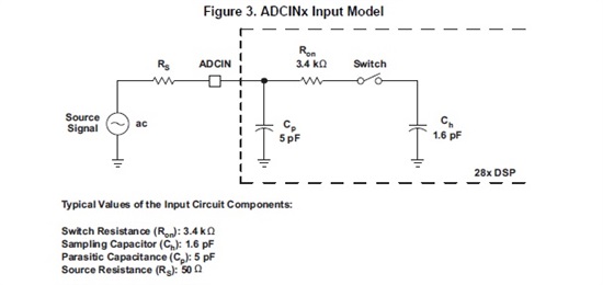
    Not sure if this will help, but as far as I understand it different ADC's will employ different methods for sampling. The image below is for the C2000 2802x series

    Adjusting the sample and hold times may help, or adding an opamp as a buffer.  Do you have details on the other ADC?

    Regards,

    Ant

  • Monica,

    The Errata is located on the product page for the device.  For example, if you have an F28027 device, you can go to the product page (http://www.ti.com/product/tms320f28027) and the Silicon Errata is linked just below the datasheet.

    If you are literally sampling the signal with both ADCs at the same time, the external ADC may be introducing noise disturbances.

    Your setting of ACQPS=6 to select 7 ADC clock cycles is correct.  You can try a larger value to see if it helps.

    -Tommy

  • Monica,

    Can you confirm that some trim is being populated by your code? Check for example that AdcRegs.ADCOFFTRIM.bit.OFFTRIM is non-zero.  If it is zero, it may be that you are initiating an ADC module reset without re-calling device calibration function.

    If the above doesn't help, can you also confirm if your F28027 device is labeled as "TMS" or "TMX"? 

  • Hi,

    AdcRegs.ADCOFFTRIM.bit.OFFTRIM is 0. When I initialize the ADC all I do is to call InitAdc(); from F2806x_Adc.c and then

    EALLOW;
       AdcRegs.ADCCTL2.bit.ADCNONOVERLAP = 1;    // Enable non-overlap mode
       AdcRegs.ADCCTL1.bit.INTPULSEPOS   = 1;    //ADCINT trips after AdcResults latch (EOC triggers ADCINT)
       
       AdcRegs.INTSEL1N2.bit.INT1E       = 1;     //Enabled ADCINT1
       AdcRegs.INTSEL1N2.bit.INT1CONT    = 0;     //Disable ADCINT1 Continuous mode
       AdcRegs.INTSEL1N2.bit.INT1SEL     = 0;    //Setup EOC0 to trigger ADCINT1 to fire
                                                 
       AdcRegs.ADCSOC0CTL.bit.CHSEL      = 3;    // set SOC0 channel select to ADC_A3 
       AdcRegs.ADCSOC1CTL.bit.CHSEL      = 5;    // set SOC1 channel select to ADC_A5
       AdcRegs.ADCSOC2CTL.bit.CHSEL      = 6;    // set SOC2 channel select to ADC_A6
       AdcRegs.ADCSOC3CTL.bit.CHSEL      = 7;    // set SOC3 channel select to ADC_A7
       
       AdcRegs.ADCSOC0CTL.bit.TRIGSEL    = 8;   // set SOC0 start trigger on EPWM2B interrupt    
       AdcRegs.ADCSOC1CTL.bit.TRIGSEL    = 8;   // set SOC1 start trigger on EPWM2B interrupt
       AdcRegs.ADCSOC2CTL.bit.TRIGSEL    = 8;   // set SOC2 start trigger on EPWM2B interrupt
       AdcRegs.ADCSOC3CTL.bit.TRIGSEL    = 8;   // set SOC3 start trigger on EPWM2B interrupt
    
       AdcRegs.ADCSOC0CTL.bit.ACQPS      = 60;     // set SOC0 S/H Window to 7 ADC Clock Cycles, (6 ACQPS plus 1)
       AdcRegs.ADCSOC1CTL.bit.ACQPS      = 60;     // set SOC1 S/H Window to 7 ADC Clock Cycles, (6 ACQPS plus 1)
       AdcRegs.ADCSOC2CTL.bit.ACQPS      = 60;     // set SOC2 S/H Window to 7 ADC Clock Cycles, (6 ACQPS plus 1)
       AdcRegs.ADCSOC3CTL.bit.ACQPS      = 60;     // set SOC3 S/H Window to 7 ADC Clock Cycles, (6 ACQPS plus 1)
    
       
       EDIS;

    I've seen that there is a function AdcOffsetSelfCal() in F2806x_Adc.c, and I've added it in the initilaization of the ADC after the call to InitAdc(); Is that correct? Because it doesn't seem to do much. I still get a 40mV difference in some ranges. (And I don't know exactly how to use this function, I was able to use it once, and then when I've changed something in the code and re-flash it, the board keeps resetting. If I comment the call to AdcOffsetSelfCal(), it works again.)

    I've checked the value indicated for 3.3V (actually on my board is 3.32V). The value indicated is 3.24V, so I've calculated a correction gain (1.024691358). The difference I get is reduced to 10-15mV. The question is now, how could I calibrate each board without using an extra ADC input channel? Plus, I can't be sure the voltage will be always 3.32V.

    My device is TMX320F28069PZA.

    Thank you,
    Monica

  • Hi Monica,

    What does your code look like for collecting the data?  You have the line:

    AdcRegs.INTSEL1N2.bit.INT1SEL = 0; //Setup EOC0 to trigger ADCINT1 to fire

    Which will set the interrupt flag or trigger the ISR when SOC0 completes.  I think you may want to set this to 3, so that you can collect the data after all 3 SOC have completed?

    I think the time when you use the offset self-calibration is fine, but you need to be careful about what settings remain after the self-calibration function runs.  If you don't overwrite them, this could leave some additional unintended ADC settings.  Really this is intended as an example of how to calibrate out the offset, and you should try to eventually work this into your sampling scheme in whatever way makes sense for your system (but for initial development it is fine to call it, just make sure to undo any changes it makes to the ADC settings that you don't want).  

    After the self-calibration function runs, the ADC offset should be very good.  You can test this by again enabling the VREFLO connection and sampling it.  After averaging, it should be less than 4 LSBs.

    Gain error is spec'ed in the datasheet.  You can try to do better than the datasheet, but calibrating out the offset is limited by other ADC spec's like linearity and Ch-to-ch gain/offset error.  

    Since you have a TMX device (not fully production qualified) you may:

    *Have no trim in the device

    *Have static trim (not a trim specific to your unit

    *Have dynamic trim (individually generated for you specific part by automated test equipment, similar to what TMS devices will have)

    In any of the above cases, the device is not guaranteed to meet datasheet specifications, but it will be progressively closer as you move down the list.

    When did you purchase this ControlCard? 

  • Hi Devin,

    I've done the change you've indicated. AdcRegs.INTSEL1N2.bit.INT1SEL = 3;

    I've ordered more ControlCard in the last years, I don't know when was this one ordered, but I've changed the card now with one having a TMS. (How will I know what I will get when I order the next one? The supplier doesn't have different part no. for these two versions. Or now all cards come with a TMS?)

    The linearity is not an issue anymore. In the complete range I get values with 20ms smaller than expected.

    Still I'm not able to use the self calibrating function, but I'll keep trying in this direction.

    To collect the data in the ADC INT I have:

    ch5  = _IQmpy(ADC_FS_VOLTAGE,_IQ12toF(AdcResult.ADCRESULT1));

    where ADC_FS_VOLTAGE is defined as:

    const float32 ADC_FS_VOLTAGE = 0.000805664;

    Regards,

    Monica

  • Monica,

    If the self calibration function is breaking the code, then you probably need to go line-by-line for the initializations that it makes and make sure your ADC initializations overwrite these.  In particular, look at the AdcConversion(void) function.

    Looking at your code above, you may need to make sure that these lines get un-done:

    AdcRegs.ADCINTSOCSEL2.bit.SOC14 = 1;

    AdcRegs.INTSEL1N2.bit.INT2SEL = 14;     //EOC14 triggers ADCINT2

    Because in this case ADCINT1 will cause SOC14 to convert and SOC14 converting will then cause the ADC to go into "ping-pong" mode.