This thread has been locked.

If you have a related question, please click the "Ask a related question" button in the top right corner. The newly created question will be automatically linked to this question.

8 Bit Data writing to individual GPIOs

Other Parts Discussed in Thread: CONTROLSUITE

I use a C28x processor.

I take some 8bit data and I want to write these 8bit data to 32bit GPIODAT register. But the order for writing is like that;

1st bit of 8 bit data should be written in GPIO16,

2nd bit of 8bit data should be written in GPIO21,

3rd bit of 8bit data should be written in GPIO22,

4th bit of 8bit data should be written in GPIO22,

5th bit of 8bit data should be written in GPIO23,

6th bit of 8bit data should be written in GPIO24,

7th bit of 8bit data should be written in GPIO25,

8th bit of 8bit data should be written in GPIO26

How can I write code for this operation ?

  • Hi,

    How can I write code for this operation ?

    Check this post out: it pertains to 4/8 bit parallel data

    http://e2e.ti.com/support/microcontrollers/c2000/f/171/t/310994.aspx

    Regards,

    Gautam

  • I already read these posts. This post is not a solution for my problem.

  • Hello,

    Don't you only need to parse each bit from 8bit data and put it in GPDAT of the related GPIO?

    For example 5th bit (bit 4) of 8bit data, you can get it like this:

    DataBit = (DataByte >> 4) & 0x01

    or

    DataBit = (DataByte & 0x10) >> 4

    Then put DataBit in GPADAT.

    About the syntax and so on, you can learn from ControlSuite examples.

    Best regards,

    Maria

  • #include <stdint.h>

    void update(uint8_t y) {

    uint16_t x = GPIODAT;  // read current bits

    x &= ~( (1UL << 16) + (0xFEUL << 20)); // mask out bits of interest

    x |= ((uint32_t) y & 1UL) << 16) + ((uint32_t) y & 0xFEUL) << 20);  // set bits

    GPIODAT = x;  // update

    }

    You'll want to disable interrupts if GPIODAT might change during this function.

    Regards,

    Bill

  • Thank you Maria and Bill.

    Actually I'm try to assign the 8bit picture data to the appropriate GPIOs to send a 8bit data to an parallel LCD. The picture data is an array (picture[8][128]).

    For this I wrote a code piece some thing like following;

    //=================================================================

    extern unsigned long picture[8][128];
    unsigned long input[8][128];

    .

    .

    .

    .

    for(y=0;y<8;y++)
        {
        for(x=0;x<64;x++)
            {
            input[y][x] = (0x07F00000 & (picture[y][x]<<19)) + (0x00010000 & (picture[y][x]<<16));
            write_data(chip1,input[y][x]);
            }
        for(x=64;x<128;x++)
            {
            input[y][x] = (0x07F00000 & (picture[y][x]<<19)) + (0x00010000 & (picture[y][x]<<16));
            write_data(chip2,input[y][x]);
             }

    //=======================================================================

    But after compiling I get the error below;

    placement fails for object ".cinit", size 0x831 (page 0).  Available ranges: RAMM0        size: 0x3b0        unused: 0x391        max hole: 0x391        OEBSTADC    line 0    1400873450911    2333

    To fix this problem I changed the size as 0x8b0 in linker command file.
     But now after compiling it gives the error below;

    C28xx: Loader: One or more sections of your program falls into a memory region that is not writable.  These regions will not actually be written to the target.  Check your linker configuration and/or memory map.

  • Well, memory size is different problem from what you asked.

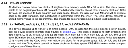
    What is your MCU? You can not change RAMM0 without checking the memory map of your MCU. You should check its memory map and change it carefully in the linker file based on what mentioned in the memory map.

    You also can attach your linker file here if you want so we can help you to review it.

    Best regards,

    Maria

  • These all are of a piece of LCD issue. I solved the problem with the GPIO parallel port writing before. And I'm thanks to all of you. For linker file I tried to change the size of RAMM0, but the total size of RAMM0 is not enough for a [8][128] array. It requires 0x841 size. So I assign RAML4 for .cinit because RAML5,6,7 for FPU math tables, and as far as I know they are not writable. So my code worked well. But I'm not sure that assigning RAML4 to .cinit is good or not ? I give the link file and my working LCD pict below:

    /*
    // TI File $Revision: /main/3 $
    // Checkin $Date: March 3, 2011   13:45:43 $
    //###########################################################################
    //
    // FILE:    28069_RAM_lnk.cmd
    //
    // TITLE:   Linker Command File For F28069 examples that run out of RAM
    //
    //          This ONLY includes all SARAM blocks on the F28069 device.
    //          This does not include flash or OTP.
    //
    //          Keep in mind that L0,L1,L2,L3 and L4 are protected by the code
    //          security module.
    //
    //          What this means is in most cases you will want to move to
    //          another memory map file which has more memory defined.
    //
    //###########################################################################
    // $TI Release: $
    // $Release Date: $
    //###########################################################################
    */

    /* ======================================================
    // For Code Composer Studio V2.2 and later
    // ---------------------------------------
    // In addition to this memory linker command file,
    // add the header linker command file directly to the project.
    // The header linker command file is required to link the
    // peripheral structures to the proper locations within
    // the memory map.
    //
    // The header linker files are found in <base>\F2806x_headers\cmd
    //
    // For BIOS applications add:      F2806x_Headers_BIOS.cmd
    // For nonBIOS applications add:   F2806x_Headers_nonBIOS.cmd
    ========================================================= */

    /* ======================================================
    // For Code Composer Studio prior to V2.2
    // --------------------------------------
    // 1) Use one of the following -l statements to include the
    // header linker command file in the project. The header linker
    // file is required to link the peripheral structures to the proper
    // locations within the memory map                                    */

    /* Uncomment this line to include file only for non-BIOS applications */
    /* -l F2806x_Headers_nonBIOS.cmd */

    /* Uncomment this line to include file only for BIOS applications */
    /* -l F2806x_Headers_BIOS.cmd */

    /* 2) In your project add the path to <base>\F2806x_headers\cmd to the
       library search path under project->build options, linker tab,
       library search path (-i).
    /*========================================================= */

    /* Define the memory block start/length for the F2806x
       PAGE 0 will be used to organize program sections
       PAGE 1 will be used to organize data sections

       Notes:
             Memory blocks on F28069 are uniform (ie same
             physical memory) in both PAGE 0 and PAGE 1.
             That is the same memory region should not be
             defined for both PAGE 0 and PAGE 1.
             Doing so will result in corruption of program
             and/or data.

             Contiguous SARAM memory blocks can be combined
             if required to create a larger memory block.
    */

    MEMORY
    {
    PAGE 0 :
       /* BEGIN is used for the "boot to SARAM" bootloader mode   */

       BEGIN       : origin = 0x000000, length = 0x000002
       RAMM0       : origin = 0x000050, length = 0x0003B0
       RAML0_L3    : origin = 0x008000, length = 0x002000     /* RAML0-3 combined for size of .text */
                                                                /* in Example_F2806xSWPrioritezedInterrupts */
       RESET       : origin = 0x3FFFC0, length = 0x000002
       FPUTABLES   : origin = 0x3FD860, length = 0x0006A0     /* FPU Tables in Boot ROM */
       IQTABLES    : origin = 0x3FDF00, length = 0x000B50    /* IQ Math Tables in Boot ROM */
       IQTABLES2   : origin = 0x3FEA50, length = 0x00008C    /* IQ Math Tables in Boot ROM */
       IQTABLES3   : origin = 0x3FEADC, length = 0x0000AA     /* IQ Math Tables in Boot ROM */

       BOOTROM    : origin = 0x3FF3B0, length = 0x000C10


    PAGE 1 :

       BOOT_RSVD   : origin = 0x000002, length = 0x00004E     /* Part of M0, BOOT rom will use this for stack */
       RAMM1       : origin = 0x000400, length = 0x000400     /* on-chip RAM block M1 */
       RAML4       : origin = 0x00A000, length = 0x002000     /* on-chip RAM block L4 */
       RAML5       : origin = 0x00C000, length = 0x002000     /* on-chip RAM block L5 */
       RAML6       : origin = 0x00E000, length = 0x002000     /* on-chip RAM block L6 */
       RAML7       : origin = 0x010000, length = 0x002000     /* on-chip RAM block L7 */
       RAML8       : origin = 0x012000, length = 0x002000     /* on-chip RAM block L8 */
       USB_RAM     : origin = 0x040000, length = 0x000800     /* USB RAM          */
    }


    SECTIONS
    {
       /* Setup for "boot to SARAM" mode:
          The codestart section (found in DSP28_CodeStartBranch.asm)
          re-directs execution to the start of user code.  */
       codestart        : > BEGIN,      PAGE = 0
       ramfuncs         : > RAMM0,      PAGE = 0
       .text            : > RAML0_L3,   PAGE = 0    
       .cinit           : > RAML4,      PAGE = 1
       .pinit           : > RAMM0,      PAGE = 0
       .switch          : > RAMM0,      PAGE = 0
       .reset           : > RESET,      PAGE = 0, TYPE = DSECT /* not used, */

       .stack           : > RAMM1,      PAGE = 1
       .ebss            : > RAML4,      PAGE = 1
       .econst          : > RAML4,      PAGE = 1
       .esysmem         : > RAML4,      PAGE = 1

       IQmath           : > RAML0_L3,   PAGE = 0
       IQmathTables     : > IQTABLES,   PAGE = 0, TYPE = NOLOAD
       
       /* Allocate FPU math areas: */
       FPUmathTables    : > FPUTABLES,  PAGE = 0, TYPE = NOLOAD
       
       DMARAML5            : > RAML5,      PAGE = 1
       DMARAML6            : > RAML6,      PAGE = 1
       DMARAML7            : > RAML7,      PAGE = 1
       DMARAML8            : > RAML8,      PAGE = 1   

      /* Uncomment the section below if calling the IQNexp() or IQexp()
          functions from the IQMath.lib library in order to utilize the
          relevant IQ Math table in Boot ROM (This saves space and Boot ROM
          is 1 wait-state). If this section is not uncommented, IQmathTables2
          will be loaded into other memory (SARAM, Flash, etc.) and will take
          up space, but 0 wait-state is possible.
       */
       /*
       IQmathTables2    : > IQTABLES2, PAGE = 0, TYPE = NOLOAD
       {

                  IQmath.lib<IQNexpTable.obj> (IQmathTablesRam)

       }
       */
       /* Uncomment the section below if calling the IQNasin() or IQasin()
          functions from the IQMath.lib library in order to utilize the
          relevant IQ Math table in Boot ROM (This saves space and Boot ROM
          is 1 wait-state). If this section is not uncommented, IQmathTables2
          will be loaded into other memory (SARAM, Flash, etc.) and will take
          up space, but 0 wait-state is possible.
       */
       /*
       IQmathTables3    : > IQTABLES3, PAGE = 0, TYPE = NOLOAD
       {

                  IQmath.lib<IQNasinTable.obj> (IQmathTablesRam)

       }
       */

    }

    /*
    //===========================================================================
    // End of file.
    //===========================================================================
    */

  • Hello,

    OZGUR POLAT said:
    I assign RAML4 for .cinit

    OZGUR POLAT said:
    But I'm not sure that assigning RAML4 to .cinit is good or not ?

    Based on datasheet of F28069, you can do it.

    If you use flash, you can put your .cinit in flash.

    So I think your problem is solved, right? Please verify the thread to mark it as solved.

    Cheers!

    Best regards,

    Maria

  • Thanks Maria, the problem was solved !

    Regards.