Because of the Thanksgiving holiday in the U.S., TI E2E™ design support forum responses may be delayed the week of November 23.

This thread has been locked.

If you have a related question, please click the "Ask a related question" button in the top right corner. The newly created question will be automatically linked to this question.

Power up sequence in DSP TMS320F28377D

Other Parts Discussed in Thread: TMS320F28377D

On page 50 of DSP TMS320F28377D dataheet has a power sequencing for digital pins.

5.6 Power Sequencing
The voltage on VDDIO should be greater than or equal to the voltage on VDD during power up. Before
powering the device, no voltage larger than 0.3 V above VDDIO should be applied to any digital pin, and no
voltage larger than 0.3 V above VDDA should be applied to any analog pin. The internal power-on-reset
circuit will ensure glitchless IOs during power up.

My issue is about analog pins. They should be powered after all DSP digital supplies are stable? Or I can power up before DSP is runnig?

And for ADC Voltage references?

And ADC inputs?

  • Hi Nedais,

    I would like you to go through this link for your answer:

    http://e2e.ti.com/support/microcontrollers/c2000/f/171/t/317699.aspx

    Regards,

    Gautam

  • Hi nedais,

    There should be no voltage applied to any analog pins (including voltage reference pins) greater that 0.3V+VDDA (analog supply).  VDDA should never be at a voltage greater than 0.3V from VDDIO. 

    This does not explicitly mean that the device needs to be powered, but that the input voltage is limited based on VDDA and VDDIO.  If you apply any voltage greater than this 0.3V delta, the device can be damaged.

    Best Regards,

    Adam

  • Previous post was edited...

  • Hi Adam Dunhoft,

    So the power sequencing for DSP should be: VDDIO(3.3V) -> VDD(1.2V) -> VDDA(3.3V). Then apply voltage any GPIOs and any Analog inputs, right?

    For digital circuit with TPS70345PWP I can ensure VDDIO(3.3V) -> VDD(1.2V) -> VDDA(3.3V) power sequencing, but for ADC inputs and Analog Voltage Reference it is dificult to garantee this, because I will need to supply all sensor after DSP start.

    In F28377D Delfino controlCARD schematic there is no power sequence for Analog Voltage References and ADC inputs.

    Thanks for support.

    nedais

  • Hi nedais,

    VDDIO and VDDA should be brought up to 3.3V together.  Typically the same source is used for VDDIO and VDDA.  As for the analog input pins, the text in the datasheet applies: "...and no voltage larger than 0.3 V above VDDA should be applied to any analog pin".

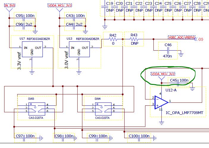
    As for the controlCARD setup, the voltage references are gated by the signal circled in green below.

    There should be no state where the voltage reference is greater than 0.3V above VDDA on this controlCARD.

    Regards,

    Adam