This thread has been locked.

If you have a related question, please click the "Ask a related question" button in the top right corner. The newly created question will be automatically linked to this question.

TMS320F28377D Advisory "ADC: ADC Input Multiplexer Connection at Beginning of Acquisition Window"

Other Parts Discussed in Thread: TMS320F28377D

Dear,

Could you please give me your advice?

Device: TMS320F28377D

sprz412b says following in "ADC: ADC Input Multiplexer Connection at Beginning of Acquisition Window",
Workaround: it may be necessary to increase the duration of the acquisition window

Question:
I'm not sure what amount should be increased.  Can you please more/some example?  Or could you please how I can figure out the increase the duration of the acquisition window?


Best regards,
Okayama


  • Okayama,

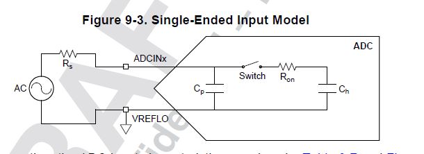
    This is not something easy to quantify.  There is a pin model of the ADC input in the TRM, SPRUHM8:

    You need Ch to charge to within 1/2 LSB of the input voltage within the tim that the switch is closed.  Neglecting Cp which is small, you can determine that you need tsample > 9*R*C, where C=Ch, R=Rs+Ron.

    You control Rs and tsample, and need to make the equation work.  Rs is the output impedance of your signal conditioning circuit (i.e. op-amp).  A very good amp will have Rs<50 Ohm, but of course that amp can be expensive.  People use less expensive amps with higher output impedance, and then have to increase tsample to make the equation hold.

    The errata is saying that you may not get the full tsample to charge your hold cap.  There can be a brief period of time where the source is not connected, but instead something else (the old channel, or Vssa) might be connected.  The errata indicates that the time of connection could be up to 5 ns, so you could subtract 5 ns from tsample in the equation:

    tsample - 5ns > 9*R*C

    I would think the above modification would handle worst case.  The errata also gives the connection resistance, but that is not needed in my opinion since you compute tsample for worst case swing on the hold capacitor anyway (i.e., from ground to full-scale input).

    Regards,

    David

  • Hi Okayama,

    David has given a pretty good overview of the thought process for analytically estimating the required S+H window.  I just wanted to add a few points:

    *In addition to Rs, there will typically be some external capacitance on the ADC input.  This could be intentional, for example as the C part of an RC low-pass filter on the input, or unintentional, for example via stray capacitance of the input traces on the PCB. Because of the channel shorting issue, this external capacitance, along with Cp, will be partially discharged in the 5ns shorting time. For the remainder of the S+H window, the signal source will have to charge both the external capacitances and the internal Ch capacitor.  The result is something like an R-C-R-C network, where you are trying to solve for when the final C will be charged to within 1/2LSBs and the second C is already partially charged.  This is possible, but not easy, to tackle analytically.  Its probably better to instead try and simulate this in SPICE.

    *Alternately, it is relatively easy to evaluate experimentally whether the S+H duration is adequate.  Configure the ADC with one channel connected to VSSA, one channel connected through your signal conditioning circuitry to a DC voltage (around mid-scale), and another channel connected directly to the same DC voltage and with a large capacitor on the pin (uF range).  Configure the first and third channels for maximum S+H duration and the second channel for minimum duration.  Use the same ADC trigger to convert all three channels in a sequence.  Observe the difference in the conversion results between the second and third channels.  Increase S+H duration of the second channel until the results match.  When evaluating the difference between the two channels, you may want to use an average of the test run multiple times to eliminate the impact of noise. Once the two channels match, try changing the first channel to VDDA instead of VSSA, and try a few different DC voltages.  

  • Devin,

    Devin Cottier said:

    The result is something like an R-C-R-C network, where you are trying to solve for when the final C will be charged to within 1/2LSBs and the second C is already partially charged.  This is possible, but not easy, to tackle analytically.  Its probably better to instead try and simulate this in SPICE.

    Yeah, you hit the nail right on the head here.  The double-RC is actually not all that complex from a math perspective.  It is just a 2nd order differential equation.  If you have values for all the Rs and Cs, you can in fact solve it quite easily (I like a good differential equation!).  But without values, it is tough.  You don't know what the roots of the equation are, and whether they are real or complex.  There are too many variables.

    Just for the record here, the tsample > 9*R*C comes from solving the first order diffy-Q obtained by neglecting Cp, and with Vo equal to (1-0.5LSB) of Vin.  Here, 0.5LSB would be, say, 0.5/4096 for a 12-bit converter for example.

    Regards,

    David