This thread has been locked.

If you have a related question, please click the "Ask a related question" button in the top right corner. The newly created question will be automatically linked to this question.

F28M35 - ADC Accuracy consistently poor.

Other Parts Discussed in Thread: CONTROLSUITE, F28M35H52C

I am using Rev B silicon and have implemented most (if not all) of the ADC-related fixes in the Errata.

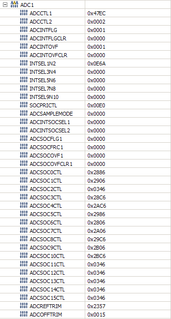
When running the code, there are values in the ADC offset registers on both modules so I know that the offset functions are running.

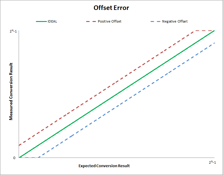
However, if I put a regulated 1.634V signal on any pin, I get a bad offset.

Using the internal voltage reference:

I should get 1.634 / 3.3 * 4096 = 2028, but I get 2012 or so.

Using the external reference (custom board, regulated supply):

I should get 1.634/3.27 = 2047, but I get 2032 or so.

This behavior is exhibited on at least 3 separate boards and the input voltage was measured by multiple separate meters.

Here is some data after 60 seconds of capturing ADC results at 2kHz, using an external 3.27V reference, and sending them over CAN:

1.634V (ADC1A2) -Average: 2032.138032

1.634V (ADC2A2) -Average: 2032.236417

1.635V (ADC1A4) -Average: 2033.18649

(Std Dev < 1 count for all 3 channels)

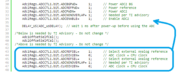
Below is the ADC Init code:

EALLOW;		// Enable EALLOW protected register access

	Adc1Regs.ADCCTL1.bit.RESET = 1;		// Reset the ADC
	Adc2Regs.ADCCTL1.bit.RESET = 1;

	asm(" NOP");
	asm(" NOP");

	(**Device_Cal)();  //Call Device Calibration to enter in factory offset, the reset above removes these values

//--- Power-up and configure the ADC
// bit 15        0:      RESET, ADC software reset, 0=no effect, 1=resets the ADC
// bit 14        0:      ADCENABLE, ADC enable, 0=disabled, 1=enabled
// bit 13        0:      ADCBSY, ADC busy, read-only
// bit 12-8      0's:    ADCBSYCHN, ADC busy channel, read-only
// bit 7         1:      ADCPWDN, ADC power down, 0=powered down, 1=powered up
// bit 6         1:      ADCBGPWD, ADC bandgap power down, 0=powered down, 1=powered up
// bit 5         1:      ADCREFPWD, ADC reference power down, 0=powered down, 1=powered up
// bit 4         0:      reserved
// bit 3         0:      ADCREFSEL, ADC reference select, 0=internal, 1=external
// bit 2         1:      INTPULSEPOS, INT pulse generation, 0=start of conversion, 1=end of conversion
// bit 1         0:      VREFLOCONV, VREFLO convert, 0=VREFLO not connected, 1=VREFLO connected to B5
// bit 0         0:      TEMPCONV, 1=temp sensor connected to ADCINA5
    Adc1Regs.ADCCTL1.bit.ADCBGPWD=	 	1;		// Power ADC1 BG
    Adc1Regs.ADCCTL1.bit.ADCREFPWD= 	1;		// Power reference
    Adc1Regs.ADCCTL1.bit.ADCPWDN=		1;		// Power ADC1
    Adc1Regs.ADCCTL2.bit.ADCNONOVERLAP= 1;		// Needed per TI advisory
    Adc1Regs.ADCCTL1.bit.ADCENABLE= 	1;		// Enable ADC1

    Adc2Regs.ADCCTL1.bit.ADCBGPWD= 		1;		// Power ADC2 BG
    Adc2Regs.ADCCTL1.bit.ADCREFPWD= 	1;		// Power reference
    Adc2Regs.ADCCTL1.bit.ADCPWDN= 		1;		// Power ADC2
    Adc2Regs.ADCCTL2.bit.ADCNONOVERLAP= 1;		// Needed per TI advisory
    Adc2Regs.ADCCTL1.bit.ADCENABLE= 	1;		// Enable ADC2

	DELAY_US(ADC_usDELAY);	// Wait 1 ms after power-up before using the ADC

/*Below is needed by TI Advisory - Do not change */
	Adc1OffsetSelfCal();
	Adc2OffsetSelfCal();
/*Above is needed by TI Advisory - Do not change */

    Adc1Regs.ADCCTL1.bit.ADCREFSEL= 	1;		// Select external Analog reference
	Adc1Regs.ADCCTL2.bit.CLKDIV2EN= 	0;		// ADC clock = CPU clock
    Adc2Regs.ADCCTL1.bit.ADCREFSEL= 	1;		// Select external Analog reference
	Adc2Regs.ADCCTL2.bit.ADCNONOVERLAP= 1;		// Needed per TI advisory
	Adc2Regs.ADCCTL2.bit.CLKDIV2EN= 	0;		// ADC clock = CPU clock

/**********************************************************************************
 * Configure SOC Triggers
 * ********************************************************************************
 * 00h = SOC priority is handled in round robin mode for all channels.
 * 01h = SOC0 is high priority, rest of channels are in round robin mode.
 * 02h = SOC0-SOC1 are high priority, SOC2-SOC15 are in round robin mode.
 * 03h = SOC0-SOC2 are high priority, SOC3-SOC15 are in round robin mode.
 * 04h = SOC0-SOC3 are high priority, SOC4-SOC15 are in round robin mode.
 * 05h = SOC0-SOC4 are high priority, SOC5-SOC15 are in round robin mode.
 * 06h = SOC0-SOC5 are high priority, SOC6-SOC15 are in round robin mode.
 * 07h = SOC0-SOC6 are high priority, SOC7-SOC15 are in round robin mode.
 * 08h = SOC0-SOC7 are high priority, SOC8-SOC15 are in round robin mode.
 * 09h = SOC0-SOC8 are high priority, SOC9-SOC15 are in round robin mode.
 * 0Ah = SOC0-SOC9 are high priority, SOC10-SOC15 are in round robin mode.
 * 0Bh = SOC0-SOC10 are high priority, SOC11-SOC15 are in round robin mode.
 * 0Ch = SOC0-SOC11 are high priority, SOC12-SOC15 are in round robin mode.
 * 0Dh = SOC0-SOC12 are high priority, SOC13-SOC15 are in round robin mode.
 * 0Eh = SOC0-SOC13 are high priority, SOC14-SOC15 are in round robin mode.
 * 0Fh = SOC0-SOC14 are high priority, SOC15 is in round robin mode.
 * 10h = All SOCs are in high priority mode, arbitrated by SOC number
 * Others = Invalid selection.*/

	Adc1Regs.SOCPRICTL.bit.SOCPRIORITY = 0x0;	// SOC priority mode - All SOC on ADC1 are round robin
	Adc2Regs.SOCPRICTL.bit.SOCPRIORITY = 0x1;	// SOC priority mode - Only SOC0 is Round Robin

/**********************************************************
 SOCx ADC Interrupt Trigger Select. Selects which, if any, ADCINT triggers SOCx.
 This field (x = 7 to 0) overrides the TRIGSEL field in the ADCSOCxCTL register.
	00 = No ADCINT will trigger SOCx. TRIGSEL field determines SOCx trigger.
	01 = ADCINT1 will trigger SOCx. TRIGSEL field is ignored.
	10 = ADCINT2 will trigger SOCx. TRIGSEL field is ignored.
	11 = Invalid selection.
***********************************************************/
	Adc1Regs.ADCINTSOCSEL1.all = 		0; 		// Disable all ADC Interrupt SOC triggers (use SOC Triggers below instead)
	Adc1Regs.ADCINTSOCSEL2.all = 		0; 		// Disable all ADC Interrupt SOC triggers (use SOC Triggers below instead)
	Adc1Regs.INTSEL1N2.bit.INT1CONT=	1; 		//Continue to run ADC even if flag is not cleared.
	Adc1Regs.INTSEL1N2.bit.INT1SEL=		10;		//Set ADCINT1 to EOC10 (DC Link voltage)
    Adc1Regs.ADCCTL1.bit.INTPULSEPOS= 	1;		// INT pulse generation = end of conversion

	Adc2Regs.ADCINTSOCSEL1.all = 		0; 		// Disable all ADC Interrupt SOC triggers (use SOC Triggers below instead)
	Adc2Regs.ADCINTSOCSEL2.all = 		0; 		// Disable all ADC Interrupt SOC triggers (use SOC Triggers below instead)
	Adc2Regs.INTSEL1N2.bit.INT2CONT=	1;		//Continue to run ADC even if flag is not cleared.
	Adc2Regs.INTSEL1N2.bit.INT2SEL=		0;		//Set ADCINT2 to EOC0 (RS Ph-Ph voltage)
    Adc2Regs.ADCCTL1.bit.INTPULSEPOS = 	1;		// INT pulse generation = end of conversion

	Adc1Regs.INTSEL1N2.bit.INT1E=		1;		//Enable Interrupt (will be EOC based on decision in ADCCTL1)
	Adc2Regs.INTSEL1N2.bit.INT2E=		1;		//Enable Interrupt (will be EOC based on decision in ADCCTL1)

	EDIS;	// Disable EALLOW protected register access
void InitSysCtrl(void)
{

    // *IMPORTANT*
    // The Device_cal function MUST be called
    // for the ADC and oscillators to function according
    // to specification. The clocks to the ADC MUST be enabled before calling
    // this function. See the device data manual and/or the ADC Reference
    // Manual for more information.

    *(unsigned int*)0x4E58 = 7; // Workaround for InitAnalogSystemClock() Advisory
    (**InitAnalogSystemClock)(ACLKDIV4);

    EALLOW;
    // Initialize the Analog Sub-System and set the clock divider to divide by 4
    while((**AnalogClockEnable)(AnalogConfig1,ADC1_ENABLE));    // Enable ADC 1
    while((**AnalogClockEnable)(AnalogConfig2,ADC2_ENABLE));    // Enable ADC 2
    (**ReadAnalogClockStatus)(AnalogConfig2);                   // Wait for AnalogClockEnable function to finish

    // Reset both ADC in case the last reset was a debugger reset (which doesn't
    // reset the ADCs
    Adc1Regs.ADCCTL1.bit.RESET = 1;
    Adc2Regs.ADCCTL1.bit.RESET = 1;
    // Wait to ensure ADCs are out of reset before device cal is called
    __asm(" nop");
    __asm(" nop");

    // Calibrate the device for temperature
    (**Device_Cal)();

    while((**AnalogClockDisable)(AnalogConfig1,ADC1_ENABLE));   // Disable ADC1
    while((**AnalogClockDisable)(AnalogConfig2,ADC2_ENABLE));   // Disable ADC2
    (**ReadAnalogClockStatus)(AnalogConfig2);                   // Wait for AnalogClockDisable function to finish
    EDIS;

    // Initialize the peripheral clocks
    InitPeripheralClocks();
}

  • Hi Will,

       What is the ADC clock speed?


      - Rick

  • Hi Will,

         How often are you running the offset calibration?


    - Rick


  • William,

    It would also be good to get conversion results at another voltage, say something near full scale but not saturating the conversion at 4095.  This will help separate how much of the error is from offset (consistent throughout input voltage range) from gain (increases with increasing input voltage).

    Regards,

    Joe

  • Joe,

    I do not have the immediate access to the equipment needed for doing that test (all ADCs are driven by conditioning circuits that require -10V -> +10v signals) but a colleague of mine did the test on a similar board:

    Average

    3919.839

    3946.458

    3928.559

    Stdev

    0.686118

    0.762135

    0.769713

    Measured

    3.194

    3.198

    3.201

    P3V3_REF

    3.29

    3.29

    3.29

    Calculated

    3976.481

    3981.461

    3985.196

    Diff

    56.64232

    35.00369

    56.63748

    Also, I was able to do a sweep with the same code on a controlCard (internal voltage reference):

    Voltage Expected ADC Actual ADC Error
    0 0 0 0
    0.4 496 447 49
    0.8 993 954 39
    1.21 1502 1461 41
    1.61 1998 1968 30
    2.01 2495 2471 24
    2.41 2991 2975 16
    2.82 3500 3479 21
    3.22 3997 3982 15
    3.3 4095 4082 13
    3.31 4095 4091 4
  • Rick, I am using the 150/75MHz configuration with the ADC clock /4, so... whatever that means!  :D

  • For now, Adc1/2OffsetCal are only run once, but the data showed here is all within the first 5 minutes of operation.  It does not seem to get better or worse over time.

  • William,

      Thank you for the additional information.  Based on the control card data there does appear to be an offset error of about -45LSB.

    While I work on getting someone to replicate your setup, I wonder if you could try moving the offset self-cal routine after the code which sets up the reference mode.  I would not expect it to make a big difference but just want to make sure.

    Also please make sure DeviceCal never executes after the self-cal runs.  It was a good deduction that self-cal is running by viewing the register contents, but DeviceCal may be storing a factory trim used for test purposes so non-zero register contents may not be enough to prove the self-cal is not getting overwritten.

    Lastly for our setup replication can you provide the ACQPS values used?

  • Joe,

    Here is the code of the Offset self-Cal routine, as you can see it sets the mode itself without setting it back. It does not really make sense to do it before since we will lose it.  I believe that the original code (when we first found this issue) did have it before and after.

    void Adc1OffsetSelfCal()
    {
        Uint16 AdcConvMean;
        EALLOW;
        Adc1Regs.ADCCTL1.bit.ADCREFSEL = 0;                     //Select internal
                                                                // reference mode
        Adc1Regs.ADCCTL1.bit.VREFLOCONV = 1;                    //Select VREFLO
                                                                // internal
                                                                // connection on B5
        Adc1ChanSelect(13);                                     //Select channel B5
                                                                // for all SOC
        Adc1Regs.ADCOFFTRIM.bit.OFFTRIM = 80;                   //Apply artificial
                                                                // offset (+80) to
                                                                // account for a
                                                                // negative offset
                                                                // that may reside
                                                                // in the ADC1 core
        AdcConvMean = Adc1Conversion();                         //Capture ADC1
                                                                // conversion on
                                                                // VREFLO
        Adc1Regs.ADCOFFTRIM.bit.OFFTRIM = 80 - AdcConvMean;     //Set offtrim
                                                                // register with new
                                                                // value (i.e remove
                                                                // artical offset
                                                                // (+80) and create
                                                                // a two's
                                                                // compliment of the
                                                                // offset error)
        Adc1Regs.ADCCTL1.bit.VREFLOCONV = 0;                    //Select external
                                                                // ADCIN5 input pin
                                                                // on B5
        EDIS;
    }

    After confirming with a global search, Device_cal runs twice total. Both snippets are detailed in the original post (it should probably be cleaned up, actually, I am not sure that the first call does anything at all.  It was a copy paste from an example project)

    Also, I have confirmed during run-time that there are non-zero contents in the Factory TRIM register. 

    All of the channels are ACQPS = 6, most are PWM timer triggered (even duplicating the first conversion due to the Advisory).

    To verify most of the above, I have attached a screen shot of the ADC1 contents at about 10 seconds after startup.

  • Thanks William,

    I would suggest moving all the ADC config code before the DELAY_US instruction and then remove the REFSEL instruction form the ADC self-cal routine.  That will ensure that the offset is calibrated using the ADC configuration used in the system and also makes sure the reference has settled before any conversions take place.

    Again, I don't expect this will have a large impact on offset necessarily, but I think it would be good practice.

    BTW where is InitAdc1/2 called with respect to InitSysCntrl?   

  • During my debugging path, I made a copy of the Adc1OffsetSelfCal function and removed the ADCREFSEL line as you have mentioned, no luck. However, this code is provided by TI, so I assumed that it worked and quickly reverted. If it is good practice, and I agree, perhaps TI could provide the code this way?

    InitSysCtrl is first, InitADC is some time later.  Both are called only once on their way to an inf loop.

    EDIT:  I changed the code to the order that you suggest and re-enabled the offset function without the refsel and there was no notable difference (2-4 counts, but mostly due to DC supply accuracy - I am using a POS).

    New Code:

    static void InitAdcDriver(void)
    {
    	EALLOW;		// Enable EALLOW protected register access
    //--- Reset the ADC module
    // Note: The ADC is already reset after a DSP reset, but this example is just showing
    // good coding practice to reset the peripheral before configuring it as you never
    // know why the DSP has started the code over again from the beginning).
    	Adc1Regs.ADCCTL1.bit.RESET = 1;		// Reset the ADC
    	Adc2Regs.ADCCTL1.bit.RESET = 1;
    
    // Must wait 2 ADCCLK periods for the reset to take effect.
    // Note that ADCCLK = SYSCLKOUT for F2802x/F2803x devices.
    	asm(" NOP");
    	asm(" NOP");
    
    	(**Device_Cal)();  //Call Device Calibration to enter in factory offset, the reset above removes these values
    
    //--- Power-up and configure the ADC
    // bit 15        0:      RESET, ADC software reset, 0=no effect, 1=resets the ADC
    // bit 14        0:      ADCENABLE, ADC enable, 0=disabled, 1=enabled
    // bit 13        0:      ADCBSY, ADC busy, read-only
    // bit 12-8      0's:    ADCBSYCHN, ADC busy channel, read-only
    // bit 7         1:      ADCPWDN, ADC power down, 0=powered down, 1=powered up
    // bit 6         1:      ADCBGPWD, ADC bandgap power down, 0=powered down, 1=powered up
    // bit 5         1:      ADCREFPWD, ADC reference power down, 0=powered down, 1=powered up
    // bit 4         0:      reserved
    // bit 3         0:      ADCREFSEL, ADC reference select, 0=internal, 1=external
    // bit 2         1:      INTPULSEPOS, INT pulse generation, 0=start of conversion, 1=end of conversion
    // bit 1         0:      VREFLOCONV, VREFLO convert, 0=VREFLO not connected, 1=VREFLO connected to B5
    // bit 0         0:      TEMPCONV, 1=temp sensor connected to ADCINA5
        Adc1Regs.ADCCTL1.bit.ADCBGPWD=	 	1;		// Power ADC1 BG
        Adc1Regs.ADCCTL1.bit.ADCREFPWD= 	1;		// Power reference
        Adc1Regs.ADCCTL1.bit.ADCPWDN=		1;		// Power ADC1
        Adc1Regs.ADCCTL2.bit.ADCNONOVERLAP= 1;		// Needed per TI advisory
        Adc1Regs.ADCCTL1.bit.ADCREFSEL= 	1;		// Select external Analog reference
        Adc1Regs.ADCCTL1.bit.ADCENABLE= 	1;		// Enable ADC1
    
        Adc2Regs.ADCCTL1.bit.ADCBGPWD= 		1;		// Power ADC2 BG
        Adc2Regs.ADCCTL1.bit.ADCREFPWD= 	1;		// Power reference
        Adc2Regs.ADCCTL1.bit.ADCPWDN= 		1;		// Power ADC2
        Adc2Regs.ADCCTL2.bit.ADCNONOVERLAP= 1;		// Needed per TI advisory
        Adc2Regs.ADCCTL1.bit.ADCREFSEL= 	1;		// Select external Analog reference
        Adc2Regs.ADCCTL1.bit.ADCENABLE= 	1;		// Enable ADC2
    
    	Adc1Regs.ADCCTL2.bit.CLKDIV2EN= 	0;		// ADC clock = CPU clock
    	Adc2Regs.ADCCTL2.bit.CLKDIV2EN= 	0;		// ADC clock = CPU clock
    
    	DELAY_US(ADC_usDELAY);	// Wait 1 ms after power-up before using the ADC
    
    /*Below is needed by TI Advisory - Do not change */
    //	Adc1OffsetSelfCal();
    //	Adc2OffsetSelfCal();
    	Adc1OffsetSelfCal_PEM();
    	Adc2OffsetSelfCal_PEM();
    /*Above is needed by TI Advisory - Do not change */
    
    /**********************************************************************************
     * Configure SOC Triggers
     * ********************************************************************************
     * 00h = SOC priority is handled in round robin mode for all channels.
     * 01h = SOC0 is high priority, rest of channels are in round robin mode.
     * 02h = SOC0-SOC1 are high priority, SOC2-SOC15 are in round robin mode.
     * 03h = SOC0-SOC2 are high priority, SOC3-SOC15 are in round robin mode.
     * 04h = SOC0-SOC3 are high priority, SOC4-SOC15 are in round robin mode.
     * 05h = SOC0-SOC4 are high priority, SOC5-SOC15 are in round robin mode.
     * 06h = SOC0-SOC5 are high priority, SOC6-SOC15 are in round robin mode.
     * 07h = SOC0-SOC6 are high priority, SOC7-SOC15 are in round robin mode.
     * 08h = SOC0-SOC7 are high priority, SOC8-SOC15 are in round robin mode.
     * 09h = SOC0-SOC8 are high priority, SOC9-SOC15 are in round robin mode.
     * 0Ah = SOC0-SOC9 are high priority, SOC10-SOC15 are in round robin mode.
     * 0Bh = SOC0-SOC10 are high priority, SOC11-SOC15 are in round robin mode.
     * 0Ch = SOC0-SOC11 are high priority, SOC12-SOC15 are in round robin mode.
     * 0Dh = SOC0-SOC12 are high priority, SOC13-SOC15 are in round robin mode.
     * 0Eh = SOC0-SOC13 are high priority, SOC14-SOC15 are in round robin mode.
     * 0Fh = SOC0-SOC14 are high priority, SOC15 is in round robin mode.
     * 10h = All SOCs are in high priority mode, arbitrated by SOC number
     * Others = Invalid selection.*/
    
    	Adc1Regs.SOCPRICTL.bit.SOCPRIORITY = 0x0;	// SOC priority mode - All SOC on ADC1 are round robin
    	Adc2Regs.SOCPRICTL.bit.SOCPRIORITY = 0x1;	// SOC priority mode - Only SOC0 is Round Robin
    
    /**********************************************************
     SOCx ADC Interrupt Trigger Select. Selects which, if any, ADCINT triggers SOCx.
     This field (x = 7 to 0) overrides the TRIGSEL field in the ADCSOCxCTL register.
    	00 = No ADCINT will trigger SOCx. TRIGSEL field determines SOCx trigger.
    	01 = ADCINT1 will trigger SOCx. TRIGSEL field is ignored.
    	10 = ADCINT2 will trigger SOCx. TRIGSEL field is ignored.
    	11 = Invalid selection.
    ***********************************************************/
    	Adc1Regs.ADCINTSOCSEL1.all = 		0; 		// Disable all ADC Interrupt SOC triggers (use SOC Triggers below instead)
    	Adc1Regs.ADCINTSOCSEL2.all = 		0; 		// Disable all ADC Interrupt SOC triggers (use SOC Triggers below instead)
    	Adc1Regs.INTSEL1N2.bit.INT1CONT=	1; 		//Continue to run ADC even if flag is not cleared.
    	Adc1Regs.INTSEL1N2.bit.INT1SEL=		10;		//Set ADCINT1 to EOC10 (DC Link voltage)
        Adc1Regs.ADCCTL1.bit.INTPULSEPOS= 	1;		// INT pulse generation = end of conversion
    
    	Adc2Regs.ADCINTSOCSEL1.all = 		0; 		// Disable all ADC Interrupt SOC triggers (use SOC Triggers below instead)
    	Adc2Regs.ADCINTSOCSEL2.all = 		0; 		// Disable all ADC Interrupt SOC triggers (use SOC Triggers below instead)
    	Adc2Regs.INTSEL1N2.bit.INT2CONT=	1;		//Continue to run ADC even if flag is not cleared.
    	Adc2Regs.INTSEL1N2.bit.INT2SEL=		0;		//Set ADCINT2 to EOC0 (RS Ph-Ph voltage)
        Adc2Regs.ADCCTL1.bit.INTPULSEPOS = 	1;		// INT pulse generation = end of conversion
    
    	Adc1Regs.INTSEL1N2.bit.INT1E=		1;		//Enable Interrupt (will be EOC based on decision in ADCCTL1)
    	Adc2Regs.INTSEL1N2.bit.INT2E=		1;		//Enable Interrupt (will be EOC based on decision in ADCCTL1)
    
    	EDIS;	// Disable EALLOW protected register access
    }

  • Hi,

    we are facing the same problem in our project.

    I've changed the TI functions because I don't want to have the standard settings changed.

    Here is my code:

    void InitAnalogSubsystem(void)
    {
      EALLOW;
      /* Initialize the Analog Sub-System and set the CLKDIV to divide by 4 *******/
      *(unsigned int*)0x4E58 = 7;              /* code needed; see silicon errata */
      (**InitAnalogSystemClock)(ACLKDIV4);
    
      /* Enable ADC 1 *************************************************************/
      while((**AnalogClockEnable)(AnalogConfig1, ADC1_ENABLE));
    
      /* Enable ADC 2, COMP1,2,3,5,6 **********************************************/
      while((**AnalogClockEnable)(AnalogConfig2, ADC2_ENABLE|COMP1_ENABLE|COMP2_ENABLE|COMP3_ENABLE|COMP5_ENABLE|COMP6_ENABLE));
    
      /* Reset both ADC in case the last reset was a debugger reset (which doesn't
         reset the ADCs ***********************************************************/
      Adc1Regs.ADCCTL1.bit.RESET = 1;
      Adc2Regs.ADCCTL1.bit.RESET = 1;
    
      /* Wait to ensure ADCs are out of reset before device_cal is called *********/
      __asm(" nop");
      __asm(" nop");
    
      /* Calibrate the device for temperature *************************************/
      (**Device_Cal)();
      EDIS;
    }
    
    void Init_Compx(volatile struct COMP_REGS *compReg)
    {
      compReg->COMPCTL.bit.COMPDACEN = 1;                         /* enable COMPx */
      compReg->COMPCTL.bit.SYNCSEL = 1;      /* synchronize output to GPIO blocks */
      compReg->COMPCTL.bit.COMPSOURCE = 0;     /* COMPx connected to internal DAC */
      compReg->COMPCTL.bit.QUALSEL = 0;         /* output passed through directly */
    
    }
    
    UINT16 Adc_Conversion(volatile struct ADC_REGS *Adr_AdcRegs,
    		              volatile struct ADC_RESULT_REGS *Adr_AdcResultRegs)
    {
      UINT16 index       = 0;
      UINT16 SampleSize  = 64;      /* set sample size (**NOTE: Sample size must be
                                       multiples of 2^x) */
      UINT32 Sum         = 0;
      UINT16 Mean        = 999;                 /* initialize mean to known value */
    
      /* run ADC Conversion *******************************************************/
      Adr_AdcRegs->ADCSOCFRC1.all = 0x0001;                   /* Force Start SOC0 */
    
      while( index < SampleSize )
      {
        /* Wait for ADCINT1 to trigger */
        while (Adr_AdcRegs->ADCINTFLG.bit.ADCINT1 == 0) {}
        Adr_AdcRegs->ADCINTFLGCLR.bit.ADCINT1 = 1;    /* clear ADCINT1 flag since */
    
        Sum   += Adr_AdcResultRegs->ADCRESULT0;                 /* sum ADC result */
    
        Adr_AdcRegs->ADCSOCFRC1.all = 0x0001;                 /* Force Start SOC0 */
        index++;
      }
    
      Mean = Sum / SampleSize;              /* Calculate average ADC sample value */
    
      return Mean;
    }
    
    void AdcOffsetCal(UINT8 AdcSel)
    {
      UINT16 AdcConvMean, i;
      volatile struct ADC_REGS *Adr_AdcRegs;
      volatile struct ADC_RESULT_REGS *Adr_AdcResultRegs;
    
      /*!!!!!!!!!!!!!!!!!!!!!!!!!!!!!!!!!!!!!!!!!!!!!!!!!!!!!!!!!!!!!!!*/
      /* temporarily workaround to minimize offset calibration failure */
      /*!!!!!!!!!!!!!!!!!!!!!!!!!!!!!!!!!!!!!!!!!!!!!!!!!!!!!!!!!!!!!!!*/
      for(i = 0; i < 500; i++)
      {
        __asm("nop");
      }
      /*---------------------------------------------------------------*/
    
      if (AdcSel == 1)
      {
        Adr_AdcRegs =&Adc1Regs;
        Adr_AdcResultRegs = &Adc1Result;
      }
      else
      {
        if (AdcSel == 2)
        {
          Adr_AdcRegs =&Adc2Regs;
          Adr_AdcResultRegs = &Adc2Result;
        }
        else
        {
          return;
        }
      }
    
      EALLOW;
      /* Select VREFLO internal connection on B5 */
      Adr_AdcRegs->ADCCTL1.bit.VREFLOCONV = 1;
    
      /* Select channel B5 for SOC 0 */
      Adr_AdcRegs->ADCSOC0CTL.bit.CHSEL   = 0xD;     /* set SOC0 select to ADC1B5 */
      Adr_AdcRegs->ADCSOC0CTL.bit.ACQPS   = 6;    /* 7 ADC CLK cycles (6 ACQPS+1) */
      Adr_AdcRegs->INTSEL1N2.bit.INT1SEL  = 0x00;         /* EOC SOC0 on ADC1INT1 */
      Adr_AdcRegs->INTSEL1N2.bit.INT1E    = 1;            /* interrupt generation */
      Adr_AdcRegs->INTSEL1N2.bit.INT1CONT = 0;  /* no interrupt to PIE, just FLAG */
    
      /* Apply artificial offset (+80) to account for a negative offset that may
         reside in the ADC core */
      Adr_AdcRegs->ADCOFFTRIM.bit.OFFTRIM = 80;
    
      /* Capture ADC conversion on VREFLO */
      AdcConvMean = Adc_Conversion(Adr_AdcRegs, Adr_AdcResultRegs);
    
      /* Set OFFTRIM register with new value (i.e remove artificial offset (+80)
         and create a two's compliment of the offset error) */
      Adr_AdcRegs->ADCOFFTRIM.bit.OFFTRIM = 80 - AdcConvMean;
    
      Adr_AdcRegs->ADCSOC0CTL.all = 0x00;            /* reset ADCSOC5CTL register */
      Adr_AdcRegs->INTSEL1N2.all  = 0x00;             /* reset INTSEL1N2 register */
    
      /* Select external ADCIN5 input pin on B5 */
      Adr_AdcRegs->ADCCTL1.bit.VREFLOCONV = 0;
      EDIS;
    }
    
    void Setup_Adc(void)
    {
      InitAnalogSubsystem();
    
      /* Configure ADC ************************************************************/
      EALLOW;
      /* power up and enable ADC1 */
      Adc1Regs.ADCCTL1.bit.ADCBGPWD  = 1;                   /* Power ADC1 bandgap */
      Adc1Regs.ADCCTL1.bit.ADCREFPWD = 1;                      /* Power reference */
      Adc1Regs.ADCCTL1.bit.ADCPWDN   = 1;                           /* Power ADC1 */
      Adc1Regs.ADCCTL1.bit.ADCENABLE = 1;                          /* Enable ADC1 */
      Adc1Regs.ADCCTL1.bit.ADCREFSEL = 1;            /* Select external reference */
    
      /* power up and enable ADC2 */
      Adc2Regs.ADCCTL1.bit.ADCBGPWD  = 1;                   /* Power ADC2 bandgap */
      Adc2Regs.ADCCTL1.bit.ADCREFPWD = 1;                      /* Power reference */
      Adc2Regs.ADCCTL1.bit.ADCPWDN   = 1;                           /* Power ADC2 */
      Adc2Regs.ADCCTL1.bit.ADCENABLE = 1;                          /* Enable ADC2 */
      Adc2Regs.ADCCTL1.bit.ADCREFSEL = 1;            /* Select external reference */
    
      /* INT pulse generation occurs 1 cycle prior to ADC result latching into its
       * result register */
      Adc1Regs.ADCCTL1.bit.INTPULSEPOS = 1;
      Adc2Regs.ADCCTL1.bit.INTPULSEPOS = 1;
    
    #ifdef VREFLO_SUP
      /* VREFLO internally connected to the ADC for sampling */
      Adc1Regs.ADCCTL1.bit.VREFLOCONV = 1;
      Adc2Regs.ADCCTL1.bit.VREFLOCONV = 0;
    #endif
    
      /* Overlap of sample is not allowed. see silicon errata */
      Adc1Regs.ADCCTL2.bit.ADCNONOVERLAP = 1;
      Adc2Regs.ADCCTL2.bit.ADCNONOVERLAP = 1;
      EDIS;
    
      /* Run ADC Zero Offset Calculation ******************************************/
      AdcOffsetCal(1);
      AdcOffsetCal(2);
      XX_Adc1VrefLoOffs = Adc1Regs.ADCOFFTRIM.bit.OFFTRIM;
      XX_Adc2VrefLoOffs = Adc2Regs.ADCOFFTRIM.bit.OFFTRIM;
    
      EALLOW;
      /* Configure ADC trigger event **********************************************/
    #if(defined ISR_EPWM2_FUNCTION)
      AnalogSysctrlRegs.TRIG1SEL.all = 0x08;         /* set EPWM2SOCA to ADCTRIG1 */
      AnalogSysctrlRegs.TRIG2SEL.all = 0x09;         /* set EPWM2SOCB to ADCTRIG2 */
    #endif
    #if(defined ISR_EPWM3_FUNCTION)
      AnalogSysctrlRegs.TRIG1SEL.all = 0x0B;         /* set EPWM3SOCA to ADCTRIG1 */
      AnalogSysctrlRegs.TRIG2SEL.all = 0x0C;         /* set EPWM3SOCB to ADCTRIG2 */
    #endif
    #if(defined ISR_EPWM4_FUNCTION)
      AnalogSysctrlRegs.TRIG1SEL.all = 0x0E;         /* set EPWM4SOCA to ADCTRIG1 */
      AnalogSysctrlRegs.TRIG2SEL.all = 0x0F;         /* set EPWM4SOCB to ADCTRIG2 */
    #endif
    #if(defined ISR_EPWM9_FUNCTION)
      AnalogSysctrlRegs.TRIG1SEL.all = 0x1D;         /* set EPWM9SOCA to ADCTRIG1 */
      AnalogSysctrlRegs.TRIG2SEL.all = 0x1E;         /* set EPWM9SOCB to ADCTRIG2 */
    #endif
    
      /* All SOCs are in high priority mode, arbitrated by SOC number *************/
      Adc1Regs.SOCPRICTL.bit.SOCPRIORITY = 0x10;
      Adc2Regs.SOCPRICTL.bit.SOCPRIORITY = 0x10;
    
      /* Configure ADC1 SOC0/1 ****************************************************/
      Adc1Regs.ADCSAMPLEMODE.bit.SIMULEN0 = 1;
      Adc1Regs.ADCSOC0CTL.bit.CHSEL   = 0x0;  /* set SOC0 select to ADC1A0/ADC1B0 */
      Adc1Regs.ADCSOC0CTL.bit.ACQPS   = 6;        /* 7 ADC CLK cycles (6 ACQPS+1) */
      Adc1Regs.ADCSOC0CTL.bit.TRIGSEL = 5;      /* SOC0 start trigger to ADCTRIG1 */
      Adc1Regs.INTSEL1N2.bit.INT1SEL  = 0x00;           /* EOC ADC1A0 on ADC1INT1 */
      Adc1Regs.INTSEL1N2.bit.INT1E    = 1;                /* interrupt generation */
      Adc1Regs.INTSEL1N2.bit.INT1CONT = 0;      /* no interrupt to PIE, just FLAG */
      Adc1Regs.INTSEL1N2.bit.INT2SEL  = 0x01;           /* EOC ADC1B0 on ADC1INT2 */
      Adc1Regs.INTSEL1N2.bit.INT2E    = 1;                /* interrupt generation */
      Adc1Regs.INTSEL1N2.bit.INT2CONT = 0;      /* no interrupt to PIE, just FLAG */
      /* Configure ADC1 SOC2 ******************************************************/
      Adc1Regs.ADCSOC2CTL.bit.CHSEL   = 0xB;         /* set SOC2 select to ADC1B3 */
      Adc1Regs.ADCSOC2CTL.bit.ACQPS   = 6;        /* 7 ADC CLK cycles (6 ACQPS+1) */
      Adc1Regs.ADCSOC2CTL.bit.TRIGSEL = 5;      /* SOC2 start trigger to ADCTRIG1 */
      Adc1Regs.INTSEL3N4.bit.INT3SEL  = 0x02;           /* EOC ADC1B3 on ADC1INT3 */
      Adc1Regs.INTSEL3N4.bit.INT3E    = 1;                /* interrupt generation */
      Adc1Regs.INTSEL3N4.bit.INT3CONT = 0;      /* no interrupt to PIE, just FLAG */
      /* Configure ADC1 SOC4 ******************************************************/
      Adc1Regs.ADCSOC4CTL.bit.CHSEL   = 0xC;         /* set SOC4 select to ADC1B4 */
      Adc1Regs.ADCSOC4CTL.bit.ACQPS   = 6;        /* 7 ADC CLK cycles (6 ACQPS+1) */
      Adc1Regs.ADCSOC4CTL.bit.TRIGSEL = 5;      /* SOC4 start trigger to ADCTRIG1 */
      Adc1Regs.INTSEL3N4.bit.INT4SEL  = 0x04;             /* EOC SOC4 on ADC1INT4 */
      Adc1Regs.INTSEL3N4.bit.INT4E    = 1;                /* interrupt generation */
      Adc1Regs.INTSEL3N4.bit.INT4CONT = 0;      /* no interrupt to PIE, just FLAG */
    #ifdef VREFLO_SUP
      /* Configure ADC1 SOC5 ******************************************************/
      Adc1Regs.ADCSOC5CTL.bit.CHSEL   = 0xD;         /* set SOC5 select to ADC1B5 */
      Adc1Regs.ADCSOC5CTL.bit.ACQPS   = 6;        /* 7 ADC CLK cycles (6 ACQPS+1) */
      Adc1Regs.ADCSOC5CTL.bit.TRIGSEL = 5;      /* SOC5 start trigger to ADCTRIG1 */
      Adc1Regs.INTSEL7N8.bit.INT7SEL  = 0x05;             /* EOC SOC5 on ADC1INT7 */
      Adc1Regs.INTSEL7N8.bit.INT7E    = 1;                /* interrupt generation */
      Adc1Regs.INTSEL7N8.bit.INT7CONT = 0;      /* no interrupt to PIE, just FLAG */
    #endif
      /* Configure ADC1 SOC6 ******************************************************/
      Adc1Regs.ADCSOC6CTL.bit.CHSEL   = 0x7;         /* set SOC6 select to ADC1A7 */
      Adc1Regs.ADCSOC6CTL.bit.ACQPS   = 6;        /* 7 ADC CLK cycles (6 ACQPS+1) */
      Adc1Regs.ADCSOC6CTL.bit.TRIGSEL = 5;      /* SOC6 start trigger to ADCTRIG1 */
      Adc1Regs.INTSEL5N6.bit.INT5SEL  = 0x06;           /* EOC ADC1A7 on ADC1INT5 */
      Adc1Regs.INTSEL5N6.bit.INT5E    = 1;                /* interrupt generation */
      Adc1Regs.INTSEL5N6.bit.INT5CONT = 0;      /* no interrupt to PIE, just FLAG */
      /* Configure ADC1 SOC7 ******************************************************/
      Adc1Regs.ADCSOC7CTL.bit.CHSEL   = 0xF;         /* set SOC6 select to ADC1B7 */
      Adc1Regs.ADCSOC7CTL.bit.ACQPS   = 6;        /* 7 ADC CLK cycles (6 ACQPS+1) */
      Adc1Regs.ADCSOC7CTL.bit.TRIGSEL = 5;      /* SOC7 start trigger to ADCTRIG1 */
      Adc1Regs.INTSEL5N6.bit.INT6SEL  = 0x07;           /* EOC ADC1B7 on ADC1INT6 */
      Adc1Regs.INTSEL5N6.bit.INT6E    = 1;                /* interrupt generation */
      Adc1Regs.INTSEL5N6.bit.INT6CONT = 0;      /* no interrupt to PIE, just FLAG */
    
      /* Configure ADC2 SOC0/1 ****************************************************/
      Adc2Regs.ADCSAMPLEMODE.bit.SIMULEN0 = 1;
      Adc2Regs.ADCSOC0CTL.bit.CHSEL   = 0x0;  /* set SOC0 select to ADC2A0/ADC2B0 */
      Adc2Regs.ADCSOC0CTL.bit.ACQPS   = 6;        /* 7 ADC CLK cycles (6 ACQPS+1) */
      Adc2Regs.ADCSOC0CTL.bit.TRIGSEL = 5;      /* SOC0 start trigger to ADCTRIG1 */
      Adc2Regs.INTSEL7N8.bit.INT7SEL  = 0x00;            /* EOC ADC2A0 on ADCINT7 */
      Adc2Regs.INTSEL7N8.bit.INT7E    = 1;                /* interrupt generation */
      Adc2Regs.INTSEL7N8.bit.INT7CONT = 0;      /* no interrupt to PIE, just FLAG */
      Adc2Regs.INTSEL7N8.bit.INT8SEL  = 0x01;            /* EOC ADC2B0 on ADCINT8 */
      Adc2Regs.INTSEL7N8.bit.INT8E    = 1;                /* interrupt generation */
      Adc2Regs.INTSEL7N8.bit.INT8CONT = 0;      /* no interrupt to PIE, just FLAG */
      /* Configure ADC2 SOC2/3 ****************************************************/
      Adc2Regs.ADCSAMPLEMODE.bit.SIMULEN2 = 1;
      Adc2Regs.ADCSOC2CTL.bit.CHSEL   = 0x3;  /* set SOC2 select to ADC2A3/ADC2B3 */
      Adc2Regs.ADCSOC2CTL.bit.ACQPS   = 6;        /* 7 ADC CLK cycles (6 ACQPS+1) */
      Adc2Regs.ADCSOC2CTL.bit.TRIGSEL = 5;      /* SOC2 start trigger to ADCTRIG1 */
      Adc2Regs.INTSEL3N4.bit.INT3SEL  = 0x02;            /* EOC ADC2A3 on ADCINT3 */
      Adc2Regs.INTSEL3N4.bit.INT3E    = 1;                /* interrupt generation */
      Adc2Regs.INTSEL3N4.bit.INT3CONT = 0;      /* no interrupt to PIE, just FLAG */
      Adc2Regs.INTSEL3N4.bit.INT4SEL  = 0x03;            /* EOC ADC2B3 on ADCINT4 */
      Adc2Regs.INTSEL3N4.bit.INT4E    = 1;                /* interrupt generation */
      Adc2Regs.INTSEL3N4.bit.INT4CONT = 0;      /* no interrupt to PIE, just FLAG */
      /* Configure ADC2 SOC4 ******************************************************/
      Adc2Regs.ADCSOC4CTL.bit.CHSEL   = 0xC;         /* set SOC4 select to ADC2B4 */
      Adc2Regs.ADCSOC4CTL.bit.ACQPS   = 6;        /* 7 ADC CLK cycles (6 ACQPS+1) */
      Adc2Regs.ADCSOC4CTL.bit.TRIGSEL = 5;      /* SOC4 start trigger to ADCTRIG1 */
      Adc2Regs.INTSEL5N6.bit.INT5SEL  = 0x04;            /* EOC ADC2B4 on ADCINT5 */
      Adc2Regs.INTSEL5N6.bit.INT5E    = 1;                /* interrupt generation */
      Adc2Regs.INTSEL5N6.bit.INT5CONT = 0;      /* no interrupt to PIE, just FLAG */
      /* Configure ADC2 SOC6 ******************************************************/
      Adc2Regs.ADCSOC6CTL.bit.CHSEL   = 0x7;         /* set SOC6 select to ADC2A7 */
      Adc2Regs.ADCSOC6CTL.bit.ACQPS   = 6;        /* 7 ADC CLK cycles (6 ACQPS+1) */
      Adc2Regs.ADCSOC6CTL.bit.TRIGSEL = 5;      /* SOC6 start trigger to ADCTRIG1 */
      Adc2Regs.INTSEL1N2.bit.INT1SEL  = 0x06;            /* EOC ADC2A7 on ADCINT1 */
      Adc2Regs.INTSEL1N2.bit.INT1E    = 1;                /* interrupt generation */
      Adc2Regs.INTSEL1N2.bit.INT1CONT = 0;      /* no interrupt to PIE, just FLAG */
      /* Configure ADC2 SOC7 ******************************************************/
      Adc2Regs.ADCSOC7CTL.bit.CHSEL   = 0xF;         /* set SOC7 select to ADC2B7 */
      Adc2Regs.ADCSOC7CTL.bit.ACQPS   = 6;        /* 7 ADC CLK cycles (6 ACQPS+1) */
      Adc2Regs.ADCSOC7CTL.bit.TRIGSEL = 5;      /* SOC7 start trigger to ADCTRIG1 */
      Adc2Regs.INTSEL1N2.bit.INT2SEL  = 0x07;            /* EOC ADC2B7 on ADCINT2 */
      Adc2Regs.INTSEL1N2.bit.INT2E    = 1;                /* interrupt generation */
      Adc2Regs.INTSEL1N2.bit.INT2CONT = 1;               /* send interrupt to PIE */
      EDIS;
    
      Adc1Regs.ADCINTOVFCLR.all = 0xFF;  /* clear all pend. int. overflows on ADC1*/
      Adc2Regs.ADCINTOVFCLR.all = 0xFF;  /* clear all pend. int. overflows on ADC2*/
    
      Adc1Regs.ADCINTFLGCLR.all = 0xFF;    /* clear all pending interrupts on ADC1*/
      Adc2Regs.ADCINTFLGCLR.all = 0xFF;    /* clear all pending interrupts on ADC2*/
    
      /* Configure Comparator Blocks **********************************************/
      Init_Compx(&Comp1Regs);                           /* initialize COMP1, XAIR */
      Init_Compx(&Comp2Regs);                           /* initialize COMP2, XAUD */
      Init_Compx(&Comp3Regs);                           /* initialize COMP3, XAIS */
      /* COMP4 currently not used */
      Init_Compx(&Comp5Regs);                           /* initialize COMP5, XAIT */
      Init_Compx(&Comp6Regs);                        /* initialize COMP6, VCC_ADC */
    
      Comp1Regs.DACVAL.all = 0x03FF;                      /* maximum DACVAL COMP1 */
      Comp2Regs.DACVAL.all = 0x03FF;                      /* maximum DACVAL COMP2 */
      Comp3Regs.DACVAL.all = 0x03FF;                      /* maximum DACVAL COMP3 */
      Comp5Regs.DACVAL.all = 0x03FF;                      /* maximum DACVAL COMP5 */
      Comp6Regs.DACVAL.all = 0x03FF;                      /* maximum DACVAL COMP6 */
    
    }


    Regards,

    Matthias

  • Just wanted to give an update: Using ControlSUITE adc_soc on a control card, my device offset looks reasonable.  Next I'll try adapting the code based on your snippets and see if I can reproduce the error you see.

    Regards,

    Joe

  • Joe,

    Thank you for your response and follow up. To ensure that we are working in a similar environment, could you answer the following questions.

    1. What version Concerto are you using?
    2. What version adc_soc are you using?
    3. What is code running on the M3 side?
    4. Can you please quantify "reasonable"?

    Before I made this post, I tried adc_soc with no improvement,  In fact, v204 does not even work (at least on my setup).

  • Using ADC_SOC (v204 with the ESTOP lines commented out) on the TI ControlCard:

    Voltage Expected ADC Adc_soc Actual Adc_soc Error
    0 0 0 0
    0.4 496 445 51
    0.8 993 945 48
    1.21 1502 1455 47
    1.61 1998 1944 54
    2.01 2495 2441 54
    2.41 2991 2928 63
    2.82 3500 3434 66
    3.22 3997 3930 67
    3.3 4095 4029 66
    3.31 4095 4041 54

    I am going to calibrate my multimeter just to eliminate yet another variable.

  • Sorry William, no new results today, but to answer your questions:

    William Perdikakis said:
    1. What version Concerto are you using?
    2. What version adc_soc are you using?
    3. What is code running on the M3 side?
    4. Can you please quantify "reasonable"?

    1. F28M35H52C, revB on a 1.0 control card

    2. V201 using CCS5

    3. Actually I wasn't even connecting to the M3

    4. Ha, you got me :)  I was seeing about 8LSB offset, but my setup was such a kludge, I wanted to get a cleaner setup before publishing numbers.

    In your first post you mention at least three boards exhibiting this problem.  Is this new development, or do you have (several) other boards which work as expected and only recently have issues?

    I don't supposed your custom board would have any ADC channel externally shorted to VREFLO or VSSA?  If so I'd be curious how the performance changes when you perform self-cal but using the externally grounded channel rather than the internal.  Also how is REFLO connected to VSSA?  How is VSSA connected to VSS?  I realize you seem to be able to replicate the issue on TI HW, but wanted to try exploring the HW side while we dig the SW side in parallel.

    regards,

    Joe

  • In the custom board application, this is the second version of this board, both versions have experienced this problem on more than 1 sample each.

    Every single ADC Channel is being used (go hard or go home, I'd say).

    VSSA1/2 are directly connected to ground.  The reference signal is actually made by a TI Part too.  :D

    Also, could you maybe try v204 and see if it even works on your setup?  Maybe the fact that mine grinds to a halt immediately (as described in my other thread) is related?

  • William,

    No appreciable difference V201 vs. V204.  Also I measured the voltage a little closer to the DUT, so offset was 5LSB/6LSB respectively.

    I'll keep plugging away.

    BTW I had no problem with V204 adc_soc once I switched the build config to RAM instead of FLASH (default).

    Regards,

    Joe

  • William,

    I'm still playing with my setups (two control cards) to see if I can replicate the issue you see on a control card, but I would like to step back to your original post for a moment.

    Before we started down the path of debugging the offset error seen on your control card setup, you originally reported your problem on custom HW which appeared to have good input signal and power supply conditioning.  If I understand correctly you were seeing about 15-16LSB of error when forcing 1.634V.  At the time I wanted to separate the gain from offset error but understandably you were limited on custom HW which took us down the road of control card data.

    My concern is that while you are clearly seeing out of spec data on the control card, the performance on your custom HW could be in spec since we can't determine how much of the error is due to offset vs. gain.  The gain spec at the full scale voltage is 60LSB/40LSB for internal/external reference mode respectively (see Table 7-1 of the DS).  At 1.634V, this scales to 30LSB/20LSB.  Additionally there could be a few more LSB due to offset.

    I'm just wondering if the root cause of the control card offset issue is not related to any concern you had based on custom HW performance, though it would still be good to resolve as well.  How much ADC error is your system designed to tolerate?  What system level problem are you seeing as a result of the ADC error?

    regards,

    Joe

  • Hi,

    I will give you some values from our project.

    After running the ADC Offset Calibration (128 samples) the values of the OFFTRIM registers are ~7 for ADC1 and ~13 for ADC2.

    To measure values between +-10V we are using external reference voltage. After Offset Calibration I measure 2040 (ADC1)  resp. 2035 (ADC2) instead of 2048 for the 0 reference value.

    Regards,

    Matthias

  • Hi Matthias,

                    Thank you for your system results.

                    It seems both you and William have a system which is sampling a signal based on a ±10V range scaled to the ADC 0-3.3V range.  One thing to point out is that the voltage you consider 0 reference point is actually a mid-voltage for the ADC.  That means error seen at that voltage cannot be attributed to offset alone.

                    In fact let’s break down the main sources of error spec’d in our DS.

    Offset error is a factor that is consistent throughout the ADC voltage range and can be positive or negative.  Please note I have exaggerated the error components well beyond our DS so they will be visible on the following plots.

     Gain error is a factor that increases linearly with increasing ADC input voltage and can be positive or negative:

    INL is a measure of the linearity of the conversion results across the input range of the ADC or put another way the deviation from the ideal after offset and gain error have been removed:

     While

    C2000 does not specifically spec Total Error in our DS, ultimately all these sources of error interact to affect the ADC.

    Simply adding the DS specs for gain, offset, and INL is a bit pessimistic since those specs are guaranteed over the normal operating range of the device and it is not likely that they will all be worst case simultaneously.  We have sometimes suggested using a square root of the sum of squares method to approximate.

    In any case, given conversation results at a single voltage point, it is difficult to separate out the sources, but based on our DS specs, gain error is typically going to dominate.  Note: gain error is spec’d at worst case input voltage (which is the max input voltage).  For a lower voltage the spec should be scaled, for example an input voltage of 1.65 could see (1.65/3.3)*60LSB = 30LSB error for internal reference mode or (1.65V/VREFHI)*40LSB for external reference mode.

    All this to say that without more information I suspect your ADC is operating within DS limits.  If the amount of error you are seeing is greater than your system can tolerate then we can potentially discuss a calibration method that might improve the gain accuracy to some degree though usually at some cost, namely you must use external reference mode and also provide a precise reference voltage to calibrate to, and TI doesn’t guarantee performance when using such methods.

    I hope this information helps, please let me know if you have questions.

  • Sorry for the delay,

    Here are some results from our board (3 phase voltage U,V,W measurements):

    Voltage Input Voltage Expected Counts   U-count Uerr V-count Verr W-count Werr
    -9.95 0.10775 133   98 35 100 -33 104 -29
    -7.95 0.41775 518   487 31 490 -28 492 -26
    -5.97 0.72465 899   870 29 874 -25 877 -22
    -4.01 1.02845 1276   1250 26 1256 -20 1257 -19
    -2.03 1.33535 1657   1635 22 1642 -15 1641 -16
    0 1.65 2048   2029 19 2035 -13 2035 -13
    2.054 1.96837 2443   2428 15 2435 -8 2433 -10
    4.07 2.28085 2831   2816 15 2825 -6 2823 -8
    5.97 2.57535 3196   3185 11 3196 0 3192 -4
    7.94 2.8807 3575   3565 10 3577 2 3574 -1
    10.02 3.2031 3975   3968 7 3981 6 3979 4

    Aside from doing 0 input (i.e. 1.65V) calibration,  what else can we do?

  • Hi William,

    If I run a linear regression in excel for your expected vs observed conversion results, I get an offset error of about -32 LSBs and a gain error of about 0.85%.

    If you can get the offset-self calibration procedure (through the internal connection to VREFLO/VSSA) integrated into your sampling code such that it is running continuously you should be able to achieve +/-4 LSBs of offset error. 

    If you also integrate periodic sampling of a 1.65V reference voltage, you should be able to (digitally via post-processing) correct the gain error to about 4 LSBs at mid-scale (8 LSBs at full scale).

    Overall, this would give you an expectation of about sqrt (4^2 + 4^2 + 8^2) =  10LSBs error (INL + offset error + gain error).


  • Devin,

    The data were generated with the VREF offset in place.

    Currently, three of our channels can safely force the 0 input (1.65V) condition and calibrate from there, but almost all of the others are subjected to time-varying signals immediately on start-up (not all are periodic).

    That said, we have no mechanism to periodically sample 1.65V. 

    What is your suggestion here? Aside from a new board design where we can disable the analog signals to the pins for a brief time to re-calibrate - what are our options?

  • Is there any information here?  This is still an issue and I would like some input as to what the expectation is for a user of this product.

    As stated above, the self-cal routine is already run on that data.

  • William,

    Where are you sampling the voltages in the attached table (at the ADC input pin where they are 0 to 3.3V range, or at the input to the signal conditioning circuitry where they are in the -10 to 10V range)?

    What instrument are you using to measure the voltage? Is the voltage DC?

    The next step would probably be to integrate the self-calibration procedure into your sampling code. (not the self calibration function, but the underlying procedure of sampling the internal REFLO connection, then adjusting the offset error)