Other Parts Discussed in Thread: TMS320F28335, UNIFLASH
Hello,
We are currently having troubles unlocking the CSM on the 28335 using the C Code examples provided in the following documents:
- TMS320x2833x, 2823x System Control and Interrupts - http://www.ti.com/lit/ug/sprufb0d/sprufb0d.pdf
- Flash API Manual v2.10
- http://processors.wiki.ti.com/index.php/C2000_Flash_Common_Issues/FAQs
Using boot control jumpers to hold processor in "Check boot mode"
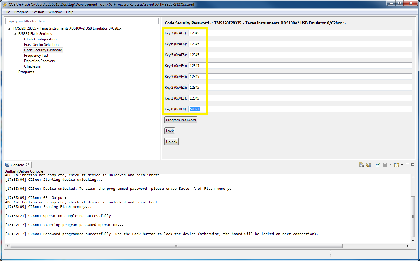
- Program CSM Password - Works correctly
- Lock CSM - Works Correctly
- Unlock CSM - Works Correctly
Using example C code in application code:
- Lock CSM - Works Correctly
- Unlock CSM - Does not work correctly
I have attached a C source file showing our lock and unlock functions. These functions are triggered by the user via our application level communications protocol and I have verified with the debugger that the passwords are correct and that the function is being executed as expected.
However the status of the CSM does not change after executing the unlock function if a password is set. I have verified this by checking CsmRegs.CSMSCR.bit.SECURE bit as well as attempting to attach the debugger.
NOTE: If no password is set, the CSM can be locked and then unlocked successfully.
Any ideas why this is occurring? I have also attached our CMD file in case the issue resides there.
/*******************************************************************************
 * DESCRIPTIION: This function returns the current status of the CSM (0 = Unlocked or 1 = Locked)
 *
 * @returns : csmStatus -> The current status of the CSM (0 = Unlocked or 1 = Locked)
 ******************************************************************************/
uint16_t OnChipFlash_getCSMStatus()
{
    return CsmRegs.CSMSCR.bit.SECURE;
}

/*----------------------------------------------------------------------------
 * Performs and unlock and verification of unlock of the flash.
 * This function is ran from RAM.
 -----------------------------------------------------------------------------*/
#pragma CODE_SECTION(OnChipFlash_unlock, "FAST_CODE") // run from ram
uint16_t OnChipFlash_unlock()
{
    volatile uint16_t temp = 0;
    volatile uint16_t result = STATUS_UNKNOWN;

    // Perform a dummy read of the password locations
    temp = CsmPwl.PSWD0;
    temp = CsmPwl.PSWD1;
    temp = CsmPwl.PSWD2;
    temp = CsmPwl.PSWD3;
    temp = CsmPwl.PSWD4;
    temp = CsmPwl.PSWD5;
    temp = CsmPwl.PSWD6;
    temp = CsmPwl.PSWD7;

    // Load the key registers with the current password
    // if they match the key values, the CSM will unlock
    EALLOW;
    CsmRegs.KEY0 = csmAccessKeys[INDEX_CSM_KEY0];
    CsmRegs.KEY1 = csmAccessKeys[INDEX_CSM_KEY1];
    CsmRegs.KEY2 = csmAccessKeys[INDEX_CSM_KEY2];
    CsmRegs.KEY3 = csmAccessKeys[INDEX_CSM_KEY3];
    CsmRegs.KEY4 = csmAccessKeys[INDEX_CSM_KEY4];
    CsmRegs.KEY5 = csmAccessKeys[INDEX_CSM_KEY5];
    CsmRegs.KEY6 = csmAccessKeys[INDEX_CSM_KEY6];
    CsmRegs.KEY7 = csmAccessKeys[INDEX_CSM_KEY7];
    EDIS;

    if(temp == temp)
    {
        ;    //NOP to remove a warning on dummy variable
    }

    // If the CSM unlocked, return success, otherwise return failure
    if(CsmRegs.CSMSCR.bit.SECURE == 0)
    {
        result = STATUS_SUCCESS;
    }
    else
    {
        result = STATUS_FAIL_CSM_LOCKED;
    }

    return result;
}
/* --COPYRIGHT--,BSD
 * Copyright (c) $(CPYYEAR), Texas Instruments Incorporated
 * All rights reserved.
 *
 * Redistribution and use in source and binary forms, with or without
 * modification, are permitted provided that the following conditions
 * are met:
 *
 * *  Redistributions of source code must retain the above copyright
 *    notice, this list of conditions and the following disclaimer.
 *
 * *  Redistributions in binary form must reproduce the above copyright
 *    notice, this list of conditions and the following disclaimer in the
 *    documentation and/or other materials provided with the distribution.
 *
 * *  Neither the name of Texas Instruments Incorporated nor the names of
 *    its contributors may be used to endorse or promote products derived
 *    from this software without specific prior written permission.
 *
 * THIS SOFTWARE IS PROVIDED BY THE COPYRIGHT HOLDERS AND CONTRIBUTORS "AS IS"
 * AND ANY EXPRESS OR IMPLIED WARRANTIES, INCLUDING, BUT NOT LIMITED TO,
 * THE IMPLIED WARRANTIES OF MERCHANTABILITY AND FITNESS FOR A PARTICULAR
 * PURPOSE ARE DISCLAIMED. IN NO EVENT SHALL THE COPYRIGHT OWNER OR
 * CONTRIBUTORS BE LIABLE FOR ANY DIRECT, INDIRECT, INCIDENTAL, SPECIAL,
 * EXEMPLARY, OR CONSEQUENTIAL DAMAGES (INCLUDING, BUT NOT LIMITED TO,
 * PROCUREMENT OF SUBSTITUTE GOODS OR SERVICES; LOSS OF USE, DATA, OR PROFITS;
 * OR BUSINESS INTERRUPTION) HOWEVER CAUSED AND ON ANY THEORY OF LIABILITY,
 * WHETHER IN CONTRACT, STRICT LIABILITY, OR TORT (INCLUDING NEGLIGENCE OR
 * OTHERWISE) ARISING IN ANY WAY OUT OF THE USE OF THIS SOFTWARE,
 * EVEN IF ADVISED OF THE POSSIBILITY OF SUCH DAMAGE.
 * --/COPYRIGHT--*/
/*
 *  ======== TMS320F28335.cmd ========
 *  Define the memory block start/length for the F28335
 *
 *! Revision History
 *! ================
 *! 26-May-2011 jv  created to support c28 generic platform.
 */

/*
 *  PAGE 0 will be used to organize program sections
 *  PAGE 1 will be used to organize data sections
 *
 *  Notes:
 *        Memory blocks on F28335 are uniform (ie same
 *        physical memory) in both PAGE 0 and PAGE 1.
 *        That is the same memory region should not be
 *        defined for both PAGE 0 and PAGE 1.
 *        Doing so will result in corruption of program
 *        and/or data.
 *
 *        L0/L1/L2 and L3 memory blocks are mirrored - that is
 *        they can be accessed in high memory or low memory.
 *        For simplicity only one instance is used in this
 *        linker file.
 */

MEMORY
{
PAGE 0:    /* Program and Data Memory */
	/*TFI         : origin = 0x338000, length = 0x007F80*/ /* first sector on-chip FLASH */
	APP         : origin = 0x300000, length = 0x038000     /* other sectors on-chip FLASH */
    CSM_RSVD    : origin = 0x33FF80, length = 0x000076, fill = 0x0000     /* Program with all 0x0000 when CSM is in use. */
    BEGIN       : origin = 0x33FFF6, length = 0x000002     /* Used for "boot to Flash" bootloader mode. */
    CSM_PWL     : origin = 0x33FFF8, length = 0x000008     /* CSM password locations in FLASH */
    OTP         : origin = 0x380400, length = 0x000400     /* on-chip OTP */
    ADC_CAL     : origin = 0x380080, length = 0x000009     /* ADC_cal function in Reserved memory */

    IQTABLES    : origin = 0x3FE000, length = 0x000b50     /* IQ Math Tables in Boot ROM */
    IQTABLES2   : origin = 0x3FEB50, length = 0x00008c     /* IQ Math Tables in Boot ROM */
    FPUTABLES   : origin = 0x3FEBDC, length = 0x0006A0     /* FPU Tables in Boot ROM */
    ROM         : origin = 0x3FF27C, length = 0x000D44     /* Boot ROM */
    RESET       : origin = 0x3FFFC0, length = 0x000002     /* part of boot ROM  */
    VECTORS     : origin = 0x3FFFC2, length = 0x00003E     /* part of boot ROM  */

PAGE 1 :   /* Data Memory */
    /*-------------------------------------------------------------------------*/
    /* RAM Ranges                                                              */
    /*-------------------------------------------------------------------------*/
    /*
     * Memory location for bootloader to pass info to the application and
     * vice versa.
     */
    REBOOT_FLAGS  : origin = 0x000000, length = 1

    /*
     * Zero wait state both program and data.
     * Ideal for placement of data structures and code that is time critical.
     */
    M01SARAM    : origin = 0x000001, length = 0x0007FF

    /*
     * Zero wait state for both program and data. This is also secure memory
     * for which the Flash API must run if the CSM is not unlocked.
     * Ideal for placement of data structures and code that is time critical.
     */
    L03SARAM    : origin = 0x008000, length = 0x004000

    /*
     * Zero wait state for data reads and writes.
     * One wait state for program reads and writes.
     * Ideal for placement of data structures.
     */
    L47SARAM    : origin = 0x00C000, length = 0x004000

    /*
     * External RAM chip.
     */
	XRAM        : origin = 0x100000, length = 0x060000

	/*
     * External RAM chip (location of System Snapshots)
     */
	XRAM_SNAPSHOT : origin = 0x160000, length = 0x020000

    /*-------------------------------------------------------------------------*/
    /*
     * This defines the memory ranges associated with the registers for the
     * memmory mapped periperhial control registers. Later data structures can
     * be foribly placed in the appropriate memmory ranged usings the sections
     * below.
     */
    /*-------------------------------------------------------------------------*/
	DEV_EMU     : origin = 0x000880, length = 0x000180     /* device emulation registers */
	FLASH_REGS  : origin = 0x000A80, length = 0x000060     /* FLASH registers */
	CSM         : origin = 0x000AE0, length = 0x000010     /* code security module registers */
    ADC_MIRROR  : origin = 0x000B00, length = 0x000010     /* ADC Results register mirror */
    XINTF       : origin = 0x000B20, length = 0x000020     /* external interface registers */
    CPU_TIMER0  : origin = 0x000C00, length = 0x000008     /* CPU Timer0 registers */
    CPU_TIMER1  : origin = 0x000C08, length = 0x000008     /* CPU Timer0 registers (CPU Timer1 & Timer2 reserved TI use)*/
    CPU_TIMER2  : origin = 0x000C10, length = 0x000008     /* CPU Timer0 registers (CPU Timer1 & Timer2 reserved TI use)*/
    PIE_CTRL    : origin = 0x000CE0, length = 0x000020     /* PIE control registers */
    PIEVECT 	: origin = 0x000D00, length = 0x000100
    DMA         : origin = 0x001000, length = 0x000200     /* DMA registers */
    MCBSPA      : origin = 0x005000, length = 0x000040     /* McBSP-A registers */
    MCBSPB      : origin = 0x005040, length = 0x000040     /* McBSP-B registers */
    ECANA       : origin = 0x006000, length = 0x000040     /* eCAN-A control and status registers */
    ECANA_LAM   : origin = 0x006040, length = 0x000040     /* eCAN-A local acceptance masks */
    ECANA_MOTS  : origin = 0x006080, length = 0x000040     /* eCAN-A message object time stamps */
    ECANA_MOTO  : origin = 0x0060C0, length = 0x000040     /* eCAN-A object time-out registers */
    ECANA_MBOX  : origin = 0x006100, length = 0x000100     /* eCAN-A mailboxes */
    ECANB       : origin = 0x006200, length = 0x000040     /* eCAN-B control and status registers */
    ECANB_LAM   : origin = 0x006240, length = 0x000040     /* eCAN-B local acceptance masks */
    ECANB_MOTS  : origin = 0x006280, length = 0x000040     /* eCAN-B message object time stamps */
    ECANB_MOTO  : origin = 0x0062C0, length = 0x000040     /* eCAN-B object time-out registers */
    ECANB_MBOX  : origin = 0x006300, length = 0x000100     /* eCAN-B mailboxes */
    EPWM1       : origin = 0x006800, length = 0x000022     /* Enhanced PWM 1 registers */
    EPWM2       : origin = 0x006840, length = 0x000022     /* Enhanced PWM 2 registers */
    EPWM3       : origin = 0x006880, length = 0x000022     /* Enhanced PWM 3 registers */
    EPWM4       : origin = 0x0068C0, length = 0x000022     /* Enhanced PWM 4 registers */
    EPWM5       : origin = 0x006900, length = 0x000022     /* Enhanced PWM 5 registers */
    EPWM6       : origin = 0x006940, length = 0x000022     /* Enhanced PWM 6 registers */
    ECAP1       : origin = 0x006A00, length = 0x000020     /* Enhanced Capture 1 registers */
    ECAP2       : origin = 0x006A20, length = 0x000020     /* Enhanced Capture 2 registers */
    ECAP3       : origin = 0x006A40, length = 0x000020     /* Enhanced Capture 3 registers */
    ECAP4       : origin = 0x006A60, length = 0x000020     /* Enhanced Capture 4 registers */
    ECAP5       : origin = 0x006A80, length = 0x000020     /* Enhanced Capture 5 registers */
    ECAP6       : origin = 0x006AA0, length = 0x000020     /* Enhanced Capture 6 registers */
    EQEP1       : origin = 0x006B00, length = 0x000040     /* Enhanced QEP 1 registers */
    EQEP2       : origin = 0x006B40, length = 0x000040     /* Enhanced QEP 2 registers */
    GPIOCTRL    : origin = 0x006F80, length = 0x000040     /* GPIO control registers */
    GPIODAT     : origin = 0x006FC0, length = 0x000020     /* GPIO data registers */
    GPIOINT     : origin = 0x006FE0, length = 0x000020     /* GPIO interrupt/LPM registers */
    SYSTEM      : origin = 0x007010, length = 0x000020     /* System control registers */
    SPIA        : origin = 0x007040, length = 0x000010     /* SPI-A registers */
    SCIA        : origin = 0x007050, length = 0x000010     /* SCI-A registers */
    XINTRUPT    : origin = 0x007070, length = 0x000010     /* external interrupt registers */
    ADC         : origin = 0x007100, length = 0x000020     /* ADC registers */
    SCIB        : origin = 0x007750, length = 0x000010     /* SCI-B registers */
    SCIC        : origin = 0x007770, length = 0x000010     /* SCI-C registers */
    I2CA        : origin = 0x007900, length = 0x000040     /* I2C-A registers */
    CSM_PWL     : origin = 0x33FFF8, length = 0x000008     /* Part of FLASHA.  CSM password locations. */
    PARTID      : origin = 0x380090, length = 0x000001     /* Part ID register location */

    /*
     * application specific. placing via linker command file saves a layer of indirection
     * which can save time during frequent code.
     */
    FPGA_CURRENT_REGS : origin = 0x208008, length = 5      /* fpga current control regs on XINTF bus */
}

/*
 *  Allocate sections to memory blocks.
 *  Note:
 *      codestart   user defined section in DSP28_CodeStartBranch.asm
 *                  used to redirect code execution when booting to flash
 */

/*
 *	http://processors.wiki.ti.com/index.php/Accessing_c_int00
 */
SECTIONS
{
	boot : > 0x300000 PAGE = 0
    {
        -l"C:\ti\xdctools_3_25_04_88\packages\ti\targets\rts2800\lib\boot.a28FP" <boot_cg.o28FP> (.text)	// TODO Modify this to use a local variable of some kind so it does not need to be hardcoded
	}
}

SECTIONS
{
	REBOOT_FLAGS_FILE : > REBOOT_FLAGS

    /* Allocate program areas: */
    .cinit              : > APP         PAGE = 0 /* constants use to initialize global vars and const in ram */
    .pinit              : > APP         PAGE = 0 /* table of constructors to be call at startup              */
    .text               : > APP         PAGE = 0 /* executable code and constants                            */
    codestart           : > BEGIN       PAGE = 0
    csmpasswds          : > CSM_PWL     PAGE = 0
    csm_rsvd            : > CSM_RSVD    PAGE = 0

    /* Allocate uninitalized data sections: */
    .taskStack          : >  L03SARAM | L47SARAM | M01SARAM PAGE = 1
    .stack              : >  L47SARAM | M01SARAM            PAGE = 1 /* the stack                   */
    .ebss               : >  XRAM 							PAGE = 1 /* global and static variables */
    .esysmem            : >  L47SARAM | M01SARAM            PAGE = 1 /* far heap                    */
    .sysmem             : >  L47SARAM | M01SARAM            PAGE = 1 /* heap                        */
    .cio                : >  L47SARAM | M01SARAM            PAGE = 1 /* buffers for System_printf   */

    /* Initalized sections go in Flash */
    .econst             : >  APP        PAGE = 0 /* far constant variabls             */
    .switch             : >  APP        PAGE = 0 /* jump tables for switch structures */
    .args               : >  APP        PAGE = 0

    /* Allocate IQ math areas: */
    IQmath              : >  APP        PAGE = 0, TYPE = NOLOAD
    IQmathTables        : >  IQTABLES   PAGE = 0, TYPE = NOLOAD
    FPUmathTables       : >  FPUTABLES  PAGE = 0, TYPE = NOLOAD

    /* Allocate ADC_cal function (pre-programmed by factory into TI reserved memory) */
    .adc_cal            : load = ADC_CAL,   PAGE = 0, TYPE = NOLOAD

    /*** The PIE Vector table is called PIEVECT by DSP/BIOS ***/
    PieVectTableFile  : > PIEVECT,     PAGE = 1,  TYPE = DSECT

    /*-------------------------------------------------------------------------*/
    /*
     * Periperhial Sections
     * This creates sections where the software define data structures that
     * represent peripherial control registers can be placed. These data
     * structures are placed over the register structures using the
     * #pragma DATA_SECTION(item, "code section"); syntax.
     */
    /*-------------------------------------------------------------------------*/
    DevEmuRegsFile    : > DEV_EMU,     PAGE = 1
    FlashRegsFile     : > FLASH_REGS,  PAGE = 1
    CsmRegsFile       : > CSM,         PAGE = 1
    AdcMirrorFile     : > ADC_MIRROR,  PAGE = 1
    XintfRegsFile     : > XINTF,       PAGE = 1
    CpuTimer0RegsFile : > CPU_TIMER0,  PAGE = 1
    CpuTimer1RegsFile : > CPU_TIMER1,  PAGE = 1
    CpuTimer2RegsFile : > CPU_TIMER2,  PAGE = 1
    PieCtrlRegsFile   : > PIE_CTRL,    PAGE = 1
    DmaRegsFile       : > DMA,         PAGE = 1
    McbspaRegsFile    : > MCBSPA,      PAGE = 1
    McbspbRegsFile    : > MCBSPB,      PAGE = 1
    ECanaRegsFile     : > ECANA,       PAGE = 1
    ECanaLAMRegsFile  : > ECANA_LAM    PAGE = 1
    ECanaMboxesFile   : > ECANA_MBOX   PAGE = 1
    ECanaMOTSRegsFile : > ECANA_MOTS   PAGE = 1
    ECanaMOTORegsFile : > ECANA_MOTO   PAGE = 1
    ECanbRegsFile     : > ECANB,       PAGE = 1
    ECanbLAMRegsFile  : > ECANB_LAM    PAGE = 1
    ECanbMboxesFile   : > ECANB_MBOX   PAGE = 1
    ECanbMOTSRegsFile : > ECANB_MOTS   PAGE = 1
    ECanbMOTORegsFile : > ECANB_MOTO   PAGE = 1
    EPwm1RegsFile     : > EPWM1        PAGE = 1
    EPwm2RegsFile     : > EPWM2        PAGE = 1
    EPwm3RegsFile     : > EPWM3        PAGE = 1
    EPwm4RegsFile     : > EPWM4        PAGE = 1
    EPwm5RegsFile     : > EPWM5        PAGE = 1
    EPwm6RegsFile     : > EPWM6        PAGE = 1
    ECap1RegsFile     : > ECAP1        PAGE = 1
    ECap2RegsFile     : > ECAP2        PAGE = 1
    ECap3RegsFile     : > ECAP3        PAGE = 1
    ECap4RegsFile     : > ECAP4        PAGE = 1
    ECap5RegsFile     : > ECAP5        PAGE = 1
    ECap6RegsFile     : > ECAP6        PAGE = 1
    EQep1RegsFile     : > EQEP1        PAGE = 1
    EQep2RegsFile     : > EQEP2        PAGE = 1
    GpioCtrlRegsFile  : > GPIOCTRL     PAGE = 1
    GpioDataRegsFile  : > GPIODAT      PAGE = 1
    GpioIntRegsFile   : > GPIOINT      PAGE = 1
	SysCtrlRegsFile   : > SYSTEM,      PAGE = 1
	SpiaRegsFile      : > SPIA,        PAGE = 1
	SciaRegsFile      : > SCIA,        PAGE = 1
	XIntruptRegsFile  : > XINTRUPT,    PAGE = 1
	AdcRegsFile       : > ADC,         PAGE = 1
	ScibRegsFile      : > SCIB,        PAGE = 1
	ScicRegsFile      : > SCIC,        PAGE = 1
	I2caRegsFile      : > I2CA,        PAGE = 1
    CsmPwlFile        : > CSM_PWL,     PAGE = 1
    PartIdRegsFile    : > PARTID,      PAGE = 1
    XRamFile          : > XRAM,        PAGE = 1
    XRamSnapshotFile  : >XRAM_SNAPSHOT,PAGE = 1

    /*XRamFile
    {
          DBM.obj(.ebss)
          DBM2GFacade.obj(.ebss)
          DBM2GFacadeScalings.obj(.ebss)
          DBM2GFacadeReadConversionFunction.obj(.ebss)
          DBM2GFacadeWriteConversionFunction.obj(.ebss)
          DBMActual.obj(.ebss)
          DBMHardLimits.obj(.ebss)
          DBMUserLimits.obj(.ebss)
          faultLog.obj(.ebss)
          faultsAndAlarms.obj(.ebss)
          monitors.obj(.ebss)
          powerup.obj(.ebss)
          taskCANInputHandler.obj(.ebss)

    }
    RUN = XRAM, PAGE = 1*/

    FPGA_CURRENT_REGS_FILE : > FPGA_CURRENT_REGS PAGE = 1

    /*-------------------------------------------------------------------------*/
    /*
     * Sections for placing flash api code in memmory.
	 */
    /*-------------------------------------------------------------------------*/
    FLASH_API:
    {
    	/*
    	 * This says to take take both the code and constants from the TI
    	 * provided Flash28335...lib file and place in this section. Since
    	 * this section is placed in L03 the linker will allocate contingent
    	 * space in L03 for this code and constants. It is up to us to copy
    	 * this content from Flash to ram via.
    	 *
    	 * extern Uint16 FLASH_API_LOADSTART;
		 * extern Uint16 FLASH_API_RUNSTART;
	     * extern Uint16 FLASH_API_LOADSIZE;
    	 * copy api from flash to ram
         * memcpy((uint16_t*)&FLASH_API_RUNSTART,
    	 *        (uint16_t*)&FLASH_API_LOADSTART,
    	 *        (unsigned long)&FLASH_API_LOADSIZE);
    	 *
    	 */
        -lFlash28335_API_V210.lib(.econst)
        -lFlash28335_API_V210.lib(.text)
        -lFlash28335_API_V210.lib(.ebss)
	}
						  /*
						   * Store the code in flash.
						   */
						  LOAD = APP,      PAGE = 0

						  /*
						   * Allocate space for all data/code assigned to this section in
						   * L03 ram. We will have to copy from flash to this memory range
						   * in code.
						   */
                          RUN  = L03SARAM, PAGE = 1

                          /*
                           * create a variable FLASH_API_LOADSTART which sits
                           * at the start of the FLASH_API section in flash
                           */
                          LOAD_START(_FLASH_API_LOADSTART),

                          /*
                           * create a var FLASH_API_LOADSIZE which is the size
                           * of the FLASH_API section in flash
                           */
                          LOAD_SIZE(_FLASH_API_LOADSIZE),

                          /*
                           * create a var FLASH_API_RUNSTART which sits
                           * at the allocated location in ram for the FLASH_API code.
                           */
                          RUN_START(_FLASH_API_RUNSTART)

    /*-------------------------------------------------------------------------*/
    /*
     * Sections for placing code in memmory for speed reasons as code runs
     * faster out of ram then flash.
	 */
    /*-------------------------------------------------------------------------*/
    FAST_VARS:
    {
    	/*
    	 * You can allocate individual functions in the section with
    	 * #pragma CODE_SECTION(function, "FAST_CODE") or you can allocate whole
    	 * sections of files as such
    	 * -lFlash28335_API_V210.lib(.econst)
         * -lFlash28335_API_V210.lib(.text)
         * for libraries

         * or
         * bearing.obj(.econst)
         * bearing.obj(.text)
         * for compiled sources.
		 *
    	 * At startup it is up to us to copy this content from Flash to ram via.
    	 * extern Uint16 FAST_CODE_LOADSTART;
		 * extern Uint16 FAST_CODE_RUNSTART;
	     * extern Uint16 FAST_CODE_LOADSIZE;
	     * copy api from flash to ram
         * memcpy((uint16_t*)&FAST_CODE_RUNSTART,
    	 *        (uint16_t*)&FAST_CODE_LOADSTART,
    	 *        (unsigned long)&FAST_CODE_LOADSIZE);
    	 *
    	 * With the variables defined below.
    	 */

        timing.obj(.ebss)
        bearing.obj(.ebss)
        fpga.obj(.ebss)
        //adc.obj(.ebss)
        ADCalculationCCM.obj(.ebss)
        AVCTables.obj(.ebss)
        avc.obj(.ebss)
     }
     RUN  = L03SARAM , PAGE = 1

    /*-------------------------------------------------------------------------*/
    /*
     * Sections for placing code in memmory for speed reasons as code runs
     * faster out of ram then flash.
	 */
    /*-------------------------------------------------------------------------*/
    FAST_CODE:
    {
    	/*
    	 * You can allocate individual functions in the section with
    	 * #pragma CODE_SECTION(function, "FAST_CODE") or you can allocate whole
    	 * sections of files as such
    	 * -lFlash28335_API_V210.lib(.econst)
         * -lFlash28335_API_V210.lib(.text)
         * for libraries

         * or
         * bearing.obj(.econst)
         * bearing.obj(.text)
         * for compiled sources.
		 *
    	 * At startup it is up to us to copy this content from Flash to ram via.
    	 * extern Uint16 FAST_CODE_LOADSTART;
		 * extern Uint16 FAST_CODE_RUNSTART;
	     * extern Uint16 FAST_CODE_LOADSIZE;
	     * copy api from flash to ram
         * memcpy((uint16_t*)&FAST_CODE_RUNSTART,
    	 *        (uint16_t*)&FAST_CODE_LOADSTART,
    	 *        (unsigned long)&FAST_CODE_LOADSIZE);
    	 *
    	 * With the variables defined below.
    	 */

        timing.obj(.econst)
        timing.obj(.text)
        bearing.obj(.econst)
        bearing.obj(.text)
//        fpga.obj(.econst) // Uncommentting this line will cause a warning if there are no const values in fpga.c or .h that need to be moved to flash.
        fpga.obj(.text)
        //adc.obj(.econst)
        //adc.obj(.text)
        //adcBMCC.obj(.econst)
        ////ADCalculationCCM.obj(.text)
        //AVCTables.obj(.econst)
        ////AVCTables.obj(.text)
        ////avc.obj(.text)
        ////monitors.obj(.text)

/*
        DBM2GFacadeReadConversionFunction.obj(.text)
		DBM2GFacade.obj(.text)
		DBM.obj(.text)
		DBM.obj(.econst)
		DBM2GFacadeWriteConversionFunction.obj(.text)
        DBM2GFacadeScalings.obj(.text)
        DBMActual.obj(.text)
        DBMHardLimits.obj(.text)
        DBMHardLimits.obj(.econst)
		RingBuffer.obj(.text)
		taskCANInputHandler.obj(.text)
		taskCANInputHandler.obj(.econst)
*/
     }
						  /*
						   * Store the code in flash.
						   */
						  LOAD = APP,       PAGE = 0

						  /*
						   * Allocate space for all data/code assigned to this section in
						   * L03 ram or M01 ram. We will have to copy from flash to this
						   * memory range in code.
						   */
                          RUN  = L03SARAM, PAGE = 1

                          /*
                           * create a variable FAST_CODE_LOADSTART which sits
                           * at the start of the FAST_CODE section in flash
                           */
                          LOAD_START(_FAST_CODE_LOADSTART),

                          /*
                           * create a var FAST_CODE_LOADSIZE which is the size
                           * of the FAST_CODE section in flash
                           */
                          LOAD_SIZE(_FAST_CODE_LOADSIZE),

                          /*
                           * create a var FAST_CODE_RUNSTART which sits
                           * at the allocated location in ram for the FAST_CODE code.
                           */
                          RUN_START(_FAST_CODE_RUNSTART)
}