Other Parts Discussed in Thread: LAUNCHXL-F28027F
Hello
I use a LAUNCHXL-F28027F and tried to day the" Example_2802xAdcSoc".
I modified it to convert channel 4 with all 16 SOCs triggered by EPMW1A
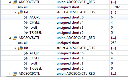
AdcRegs.ADCSOC0CTL.bit.CHSEL = 4; //set SOC0 channel select to ADCINA4
...
AdcRegs.ADCSOC15CTL.bit.CHSEL = 4; //set SOC0 channel select to ADCINA4
and
AdcRegs.ADCSOC0CTL.bit.TRIGSEL = 5;
..
AdcRegs.ADCSOC15CTL.bit.TRIGSEL = 5;
I enabled the GPIOs for the pwm outputs and toggle GPIO1 every call of the adc_isr routine.
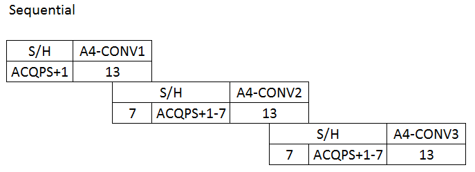
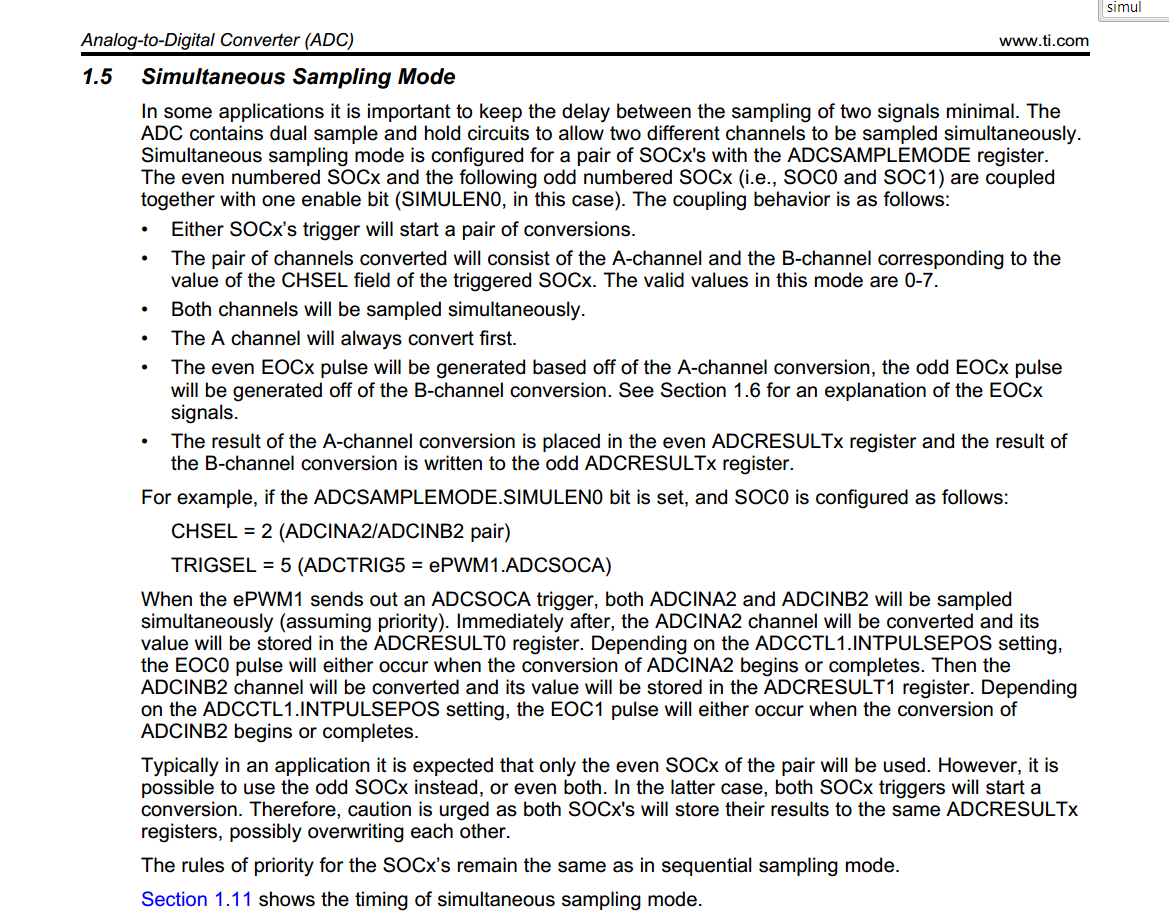
If I set the single sampe mode with
AdcRegs.ADCSAMPLEMODE.bit.SIMULEN0 = 0; // single sample mode
for all SIMULEN0 ... SIMULEN14.
it needs about 4us seconds between the SOC (EPwm1Regs.ETSEL.bit.SOCASEL = ET_CTRU_CMPA; // Select SOC from from CPMA on upcount)
and the pin toggle on GPIO1 (adc_isr => AdcRegs.INTSEL1N2.bit.INT1SEL = 15; //setup EOC15 to trigger ADCINT1 to fire)
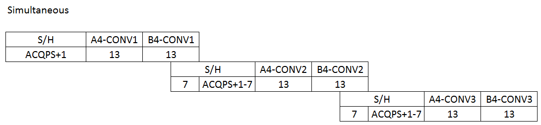
But if I enable the simultaneous sampling mode (SIMULEN0 ... SIMULEN14 = 1) it needs about 7us to toggle GPIO1.
Why? I expect nearly half the time of the single sample mode! What did I missed?
Kind regards
René