HI all
I am trying to implement CAN transmission using CAN interrupts.I was initially successfull in establishing the same and now suddenly the program has stopped working.I had been trying to debug it and find out where it went wrong from last few days.But in vain.
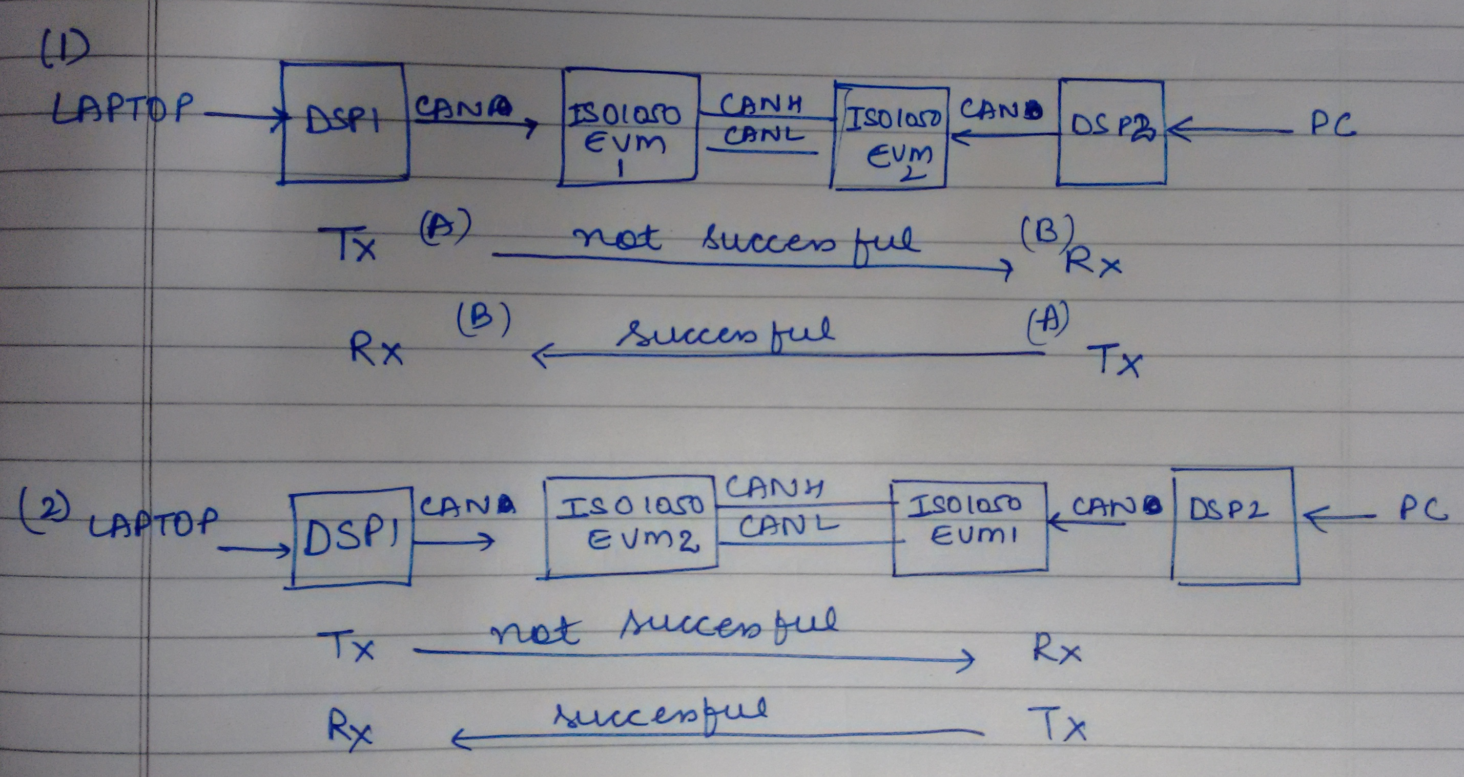
I have checked the hardware,it seems fine.As normal CAN transmission without interrupts work.
I am attaching the code for transmitter side below,I am using F28335:
// TI File $Revision: /main/2 $
// Checkin $Date: July 30, 2009   18:44:23 $
//###########################################################################
//
// FILE:    Example_2833xECanBack2Back.c
//
// TITLE:   DSP2833x eCAN Back-to-back transmission and reception in
//          SELF-TEST mode
//
// ASSUMPTIONS:
//
//    This program requires the DSP2833x header files.
//
//    This progrm uses the peripheral's self test mode.
//    Other then boot mode configuration, no other hardware configuration
//    is required.
//
//    As supplied, this project is configured for "boot to SARAM"
//    operation.  The 2833x Boot Mode table is shown below.
//    For information on configuring the boot mode of an eZdsp,
//    please refer to the documentation included with the eZdsp,
//
//       $Boot_Table:
//
//         GPIO87   GPIO86     GPIO85   GPIO84
//          XA15     XA14       XA13     XA12
//           PU       PU         PU       PU
//        ==========================================
//            1        1          1        1    Jump to Flash
//            1        1          1        0    SCI-A boot
//            1        1          0        1    SPI-A boot
//            1        1          0        0    I2C-A boot
//            1        0          1        1    eCAN-A boot
//            1        0          1        0    McBSP-A boot
//            1        0          0        1    Jump to XINTF x16
//            1        0          0        0    Jump to XINTF x32
//            0        1          1        1    Jump to OTP
//            0        1          1        0    Parallel GPIO I/O boot
//            0        1          0        1    Parallel XINTF boot
//            0        1          0        0    Jump to SARAM	    <- "boot to SARAM"
//            0        0          1        1    Branch to check boot mode
//            0        0          1        0    Boot to flash, bypass ADC cal
//            0        0          0        1    Boot to SARAM, bypass ADC cal
//            0        0          0        0    Boot to SCI-A, bypass ADC cal
//                                              Boot_Table_End$
//
// DESCRIPTION:
//
//    This test transmits data back-to-back at high speed without
//    stopping.
//    The received data is verified. Any error is flagged.
//    MBX0 transmits to MBX16, MBX1 transmits to MBX17 and so on....
//    This program illustrates the use of self-test mode
//
//###########################################################################
// Original Author H.J.
//
// $TI Release: 2833x/2823x Header Files V1.32 $
// $Release Date: June 28, 2010 $
//###########################################################################

#include "DSP28x_Project.h"     // Device Headerfile and Examples Include File

interrupt void adc_isr(void);
interrupt void ecan1_isr(void);
void can_enable_int(void);
// Prototype statements for functions found within this file.


// Global variable for this example

Uint16 loopcount = 0;
Uint16 ConversionCount = 0;
Uint16 Voltage1[32];
Uint16 Voltage2[32];
float Va=0,V1=0,sum =0,Vb=0;
int b=0,c=0,d=0,e=0;

struct ECAN_REGS ECanaShadow;
void main(void)
{

   // eCAN control registers require read/write access using 32-bits.  Thus we
// will create a set of shadow registers for this example.  These shadow
// registers will be used to make sure the access is 32-bits and not 16.

// Step 1. Initialize System Control:
// PLL, WatchDog, enable Peripheral Clocks
// This example function is found in the DSP2833x_SysCtrl.c file.
   InitSysCtrl();

   //EALLOW;
   //SysCtrlRegs.WDCR = 0x00AF;
  // EDIS;

   EALLOW;
      #if (CPU_FRQ_150MHZ)     // Default - 150 MHz SYSCLKOUT
        #define ADC_MODCLK 0x3 // HSPCLK = SYSCLKOUT/2*ADC_MODCLK2 = 150/(2*3)   = 25.0 MHz
      #endif
   EDIS;

   // Define ADCCLK clock frequency ( less than or equal to 25 MHz )
      // Assuming InitSysCtrl() has set SYSCLKOUT to 150 MHz
      EALLOW;
      SysCtrlRegs.HISPCP.all = ADC_MODCLK;
      EDIS;

// Step 2. Initalize GPIO:
// This example function is found in the DSP2833x_Gpio.c file and
// illustrates how to set the GPIO to it's default state.
// InitGpio();  // Skipped for this example

// For this example, configure CAN pins using GPIO regs here
// This function is found in DSP2833x_ECan.c
   InitECanGpio();
   InitECan();


// Step 3. Clear all interrupts and initialize PIE vector table:
// Disable CPU interrupts
   DINT;

// Initialize PIE control registers to their default state.
// The default state is all PIE interrupts disabled and flags
// are cleared.
// This function is found in the DSP2833x_PieCtrl.c file.
   InitPieCtrl();

// Disable CPU interrupts and clear all CPU interrupt flags:
   IER = 0x0000;
   IFR = 0x0000;

// Initialize the PIE vector table with pointers to the shell Interrupt
// Service Routines (ISR).
// This will populate the entire table, even if the interrupt
// is not used in this example.  This is useful for debug purposes.
// The shell ISR routines are found in DSP2833x_DefaultIsr.c.
// This function is found in DSP2833x_PieVect.c.
   InitPieVectTable();


   // Interrupts that are used in this example are re-mapped to
   // ISR functions found within this file.
      EALLOW;  // This is needed to write to EALLOW protected register
      PieVectTable.ADCINT = &adc_isr;
      EDIS;    // This is needed to disable write to EALLOW protected registers


      EALLOW;	// This is needed to write to EALLOW protected registers
      PieVectTable.ECAN1INTA = &ecan1_isr;
      EDIS;

   // Step 4. Initialize all the Device Peripherals:
   // This function is found in DSP2833x_InitPeripherals.c
   // InitPeripherals(); // Not required for this example
      InitAdc();  // For this example, init the ADC
      EnableInterrupts();
      can_enable_int();
      // Step 5. User specific code, enable interrupts:


      // Configure GPIO32 as a GPIO output pin
         EALLOW;
         GpioCtrlRegs.GPAMUX2.bit.GPIO31 = 0;//selecting pin as GPIO
         GpioCtrlRegs.GPADIR.bit.GPIO31 = 1;//setting the pin as output pin
           EDIS;

           PieCtrlRegs.PIECTRL.bit.ENPIE = 1;

           // Enables PIE to drive a pulse into the CPU
            PieCtrlRegs.PIEACK.all = 0xFFFF;

           // Enable ADCINT in PIE
              PieCtrlRegs.PIEIER1.bit.INTx6 = 1;
              IER |= M_INT1; // Enable CPU Interrupt 1
              EINT;          // Enable Global interrupt INTM
              ERTM;          // Enable Global realtime interrupt DBGM

              PieCtrlRegs.PIEIER9.bit.INTx6=1;     // PIE Group 9, INT6
              IER |= M_INT9; // Enable CPU Interrupt 1
              EINT;          // Enable Global interrupt INTM
              ERTM;
              // Configure ADC
                 AdcRegs.ADCMAXCONV.all = 0x0001;       // Setup 2 conv's on SEQ1
                 AdcRegs.ADCCHSELSEQ1.bit.CONV00 = 0x3; // Setup ADCINA3 as 1st SEQ1 conv.
                 AdcRegs.ADCCHSELSEQ1.bit.CONV01 = 0x2; // Setup ADCINA2 as 2nd SEQ1 conv.
                 AdcRegs.ADCTRL2.bit.EPWM_SOCA_SEQ1 = 1;// Enable SOCA from ePWM to start SEQ1
                 AdcRegs.ADCTRL2.bit.INT_ENA_SEQ1 = 1;  // Enable SEQ1 interrupt (every EOS)

              // Assumes ePWM1 clock is already enabled in InitSysCtrl();
                 EPwm1Regs.ETSEL.bit.SOCAEN = 1;        // Enable SOC on A group
                 EPwm1Regs.ETSEL.bit.SOCASEL = 4;       // Select SOC from from CPMA on upcount
                 EPwm1Regs.ETPS.bit.SOCAPRD = 1;        // Generate pulse on 1st event
                 EPwm1Regs.CMPA.half.CMPA = 0x0080;	  // Set compare A value
                 EPwm1Regs.TBPRD = 0xFFFF;              // Set period for ePWM1
                 EPwm1Regs.TBCTL.bit.CTRMODE = 0;		  // count up and start

                 /* Write to the MSGID field  */

                        ECanaMboxes.MBOX1.MSGID.all     = 0x00002005;
                        ECanaMboxes.MBOX1.MSGID.bit.IDE = 1;  // standard Identifier


                        /* Configure Mailbox under test as a Transmit mailbox */

                            ECanaShadow.CANMD.all = ECanaRegs.CANMD.all;
                            ECanaShadow.CANMD.bit.MD1 = 0; //transciever
                            ECanaRegs.CANMD.all = ECanaShadow.CANMD.all;


                            ECanaMboxes.MBOX1.MSGCTRL.all  = 0;

                            ECanaMboxes.MBOX1.MSGCTRL.bit.DLC = 8;


                            /* Enable Mailbox under test */

                            ECanaShadow.CANME.all = ECanaRegs.CANME.all;
                            ECanaShadow.CANME.bit.ME1 = 1;
                            ECanaRegs.CANME.all = ECanaShadow.CANME.all;


    // Begin transmitting
    for(;;)
    {
b=1;


    	    							ECanaMboxes.MBOX1.MDL.all =  Voltage1[ConversionCount];
    	    	           	           ECanaMboxes.MBOX1.MDH.all = 12345678;
    	    	           	        GpioDataRegs.GPADAT.bit.GPIO31 = 1;


    	    	           	     sum += Voltage1[ConversionCount];

    	    	           	        	    	           	         if(ConversionCount == 31)
    	    	           	        	    	           	         {

    	    	           	        	    	           	            V1 = sum/ConversionCount;
    	    	           	        	    	           	            Va = (V1 * 3)/(4096);
    	    	           	        	    	           	            Vb = Va/0.05264;
    	    	           	        	    	           	            sum = 0;

    	    	           	        	    	           	       	    ConversionCount = 0;
    	    	           	        	    	           	         }
    	    	           	        	    	           	         else ConversionCount++;

    	    	           	         ECanaShadow.CANTRS.all = 0;
    	    	    	              ECanaShadow.CANTRS.bit.TRS1 = 1;             // Set TRS for mailbox under test
    	    	    	              ECanaRegs.CANTRS.all = ECanaShadow.CANTRS.all;


    	    	    	              do
    	    	    	               {

    	    	    	               ECanaShadow.CANTA.all = ECanaRegs.CANTA.all;
    	    	    	               } while(ECanaShadow.CANTA.bit.TA1 == 0 );   // Wait for TA5 bit to be set..

    	    	    	              GpioDataRegs.GPADAT.bit.GPIO31 = 0;// clears the GPIO31

    	    	    	              loopcount ++;

b=2;


    	       }
    	        asm(" ESTOP0");  // Stop here

    	}

interrupt void  adc_isr(void)
{
c=1;
  Voltage1[ConversionCount] = AdcRegs.ADCRESULT0 >>4;
  //Voltage2[ConversionCount] = AdcRegs.ADCRESULT1 >>4;


  // Reinitialize for next ADC sequence
  AdcRegs.ADCTRL2.bit.RST_SEQ1 = 1;         // Reset SEQ1
  AdcRegs.ADCST.bit.INT_SEQ1_CLR = 1;       // Clear INT SEQ1 bit
  PieCtrlRegs.PIEACK.all = PIEACK_GROUP1;   // Acknowledge interrupt to PIE
c=2;
  return;
}

void can_enable_int()
{
	d=1;
  /* Configure CAN interrupts */
 ECanaShadow.CANMIL.all = ECanaRegs.CANMIL.all;
 ECanaShadow.CANMIL.all = 0xFFFFFFFF; // Interrupts asserted on eCAN0INT and eCAN1INT
 ECanaRegs.CANMIL.all = ECanaShadow.CANMIL.all;

 /* Disable register-write protection, since CANGIM and CANMIM registers are EALLOW protected */
 EALLOW;

 ECanaShadow.CANMIM.all = ECanaRegs.CANMIM.all;

 ECanaShadow.CANMIM.all = 0xFFFFFFFF; // Enable interrupts for all mailboxes
 ECanaRegs.CANMIM.all = ECanaShadow.CANMIM.all;

 ECanaShadow.CANGIM.all = ECanaRegs.CANGIM.all;
 ECanaShadow.CANGIM.all = 0;
 ECanaShadow.CANGIM.bit.GIL = 1;   // to insert intr on CANGIF1
 ECanaShadow.CANGIM.bit.AAIM = 1;  // Enable Abort Interrupt
 ECanaShadow.CANGIM.bit.WDIM = 1;  // Enable Watchdog Timer Interrupt
 ECanaShadow.CANGIM.bit.WUIM = 1;  // Enable
 ECanaShadow.CANGIM.bit.BOIM = 1;  // Enable
 ECanaShadow.CANGIM.bit.EPIM = 1;  // Enable
 ECanaShadow.CANGIM.bit.WLIM = 1;  // Enable
 ECanaShadow.CANGIM.bit.I0EN = 1;  // Enable eCAN1INT or eCAN0INT
 ECanaShadow.CANGIM.bit.I1EN = 1;
 ECanaRegs.CANGIM.all = ECanaShadow.CANGIM.all;
 /* ---------- eCANA Peripheral Mailboxes Enable - End ------------ */

  /* Enable register-write protection */
 EDIS;
d=2;
 }

/*---------------------- DSP28xx_PieCtrl.c - End -------------------------*/


/*---------------------- DSP28xx_DefaultISR.c - Start -------------------------*/

interrupt void ecan1_isr(void)  // eCAN-A
{
e=1;
switch(ECanaRegs.CANGIF1.bit.MIV1)
 {

case 1 : // Mailbox 2 - Command Transmitting Control Parameters
{

   	    ECanaShadow.CANTA.all = 0;

   	    ECanaShadow.CANTA.bit.TA1 = 1;               // Clear TA5

   	    ECanaRegs.CANTA.all = ECanaShadow.CANTA.all;
   	 PieCtrlRegs.PIEACK.all = PIEACK_GROUP9;   // Acknowledge interrupt to PIE


}
 default :

break;

e=2;
}
}


//===========================================================================
// No more.
//===========================================================================
When I run this now,MBOX1 MDL/MDH registers donot update the value from ADC voltage.WHen i halt the program I find it stuck at the do while loop waiting for TA to set.
Now when i remove this loop transmision takes place CANTA1 sets to 1 but at the reciever side even though transmission and reception is correct,but CANRMP register does not set.
Kindly give in your inputs and help sort this issue.
Thanks & Regards
Sneha