This thread has been locked.

If you have a related question, please click the "Ask a related question" button in the top right corner. The newly created question will be automatically linked to this question.

emif1_16bit_sdram_dma_cpu01 example issue on F28377d

Hi,

I tested "emif1_16bit_sdram_dma_cpu01" example on the same Micron SDRAM as mentioned in the example. I also tested another brand SDRAM (programmed timing registers based on SDRAM data_sheet). I have the same issue with these two SDRAMs.

On each row, every 0x40 location has correlation. For example, on row 0, location 0x80000000, 0x80000040, 0x80000080 and 0x8000000c0 have correlation. If writing to one location of them, others will also change to the same value. Does anyone know what may cause this problem? Thanks in advance.
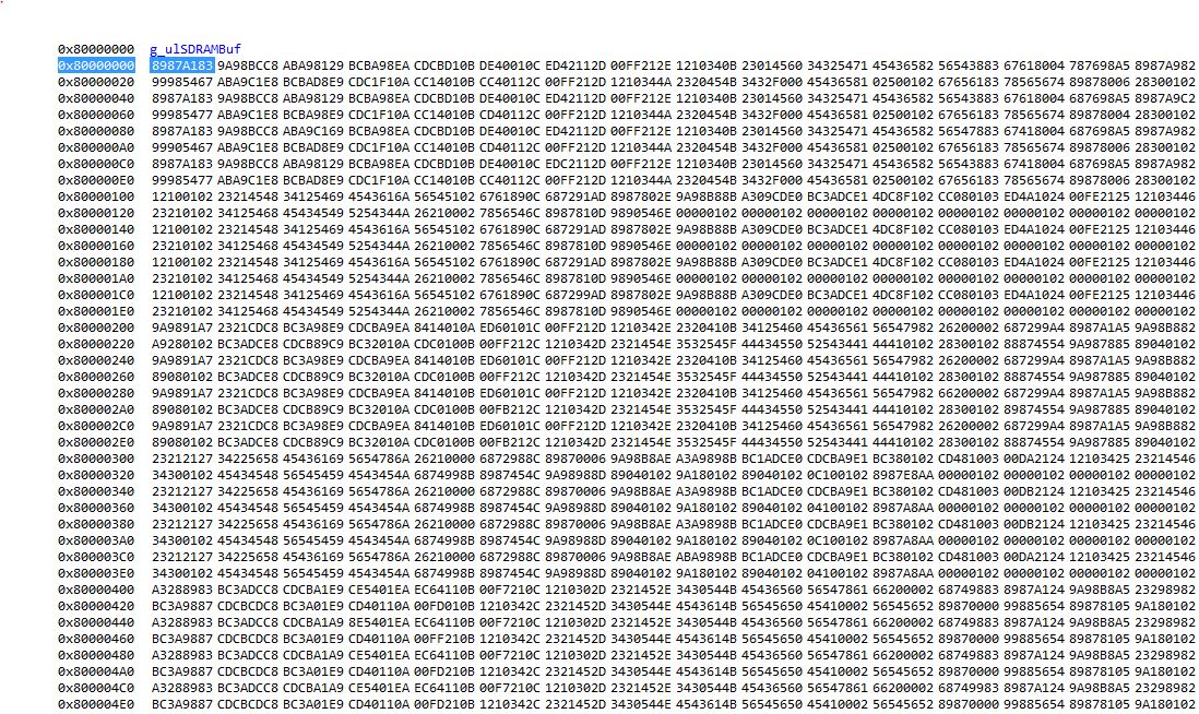
Xiaowei

  • Hi Xiaowei,

    Could you check if you see same issue for next column address?

    Regards,

    Vivek Singh

  • Hi Vivek,

    Do you mean to check next row? The issue happens on every row.

    On each row, address 0x8XXXXXXX, (0x8XXXXXXX+0x40),(0x8XXXXXXX+0x80) and address (0x8XXXXXXX+0xc0) have correlations.

    Xiaowei

  • Hi Xiaowei,

    Sorry, yes I meant next Row address.

    I understand that row 0 address 0x0 and address 0x40 have same value (correlation) but does row 1 address 0x0 also has same data as row 0 address 0x0/0x40 or you are able to update that with different data value which will again have correlation with row 1 address 0x40/0x80 and so on.

    Example code works fine on our validation setup. Is there any change made in this example while porting to your application?

    Can you verify that all the GPIO pinmux setting for EMIF is done correctly by looking at the value of these registers in CCS memory watch window.

    Regards,

    Vivek Singh

  • Hi Xiaowei,

    I re-looked at the memory snapshot you sent earlier and got answer to my Ist question. It seems like address line A6/A7 are stuck to one specific value and not changing.

    Please confirm the pinmux configuration for these pins by  looking at the value of GPIO mux registers in CCS memory watch window.

    Regards,

    Vivek Singh

  • Hi Vivek,

    Thanks for your time. I have checked the values of A6(GPIO46) and A7(GPIO47) using both of GpioDataRegs  and oscilloscope. I found an interesting thing.

    When running that EMIF example code, Gpio46 and Gpio47 showed value '1' from CCS register window(GpioDataRegs), but scope measured '0' on docking station and control card.

    Then, I run blinky_cpu01 example on GPIO47, the physical pin on control card always '0'.

    So I am thinking the control card may be have a defect on GPIO46 and 47. Do you have any thought about this?  Thanks.

    Xiaowei

  • Hi Xiaowei,

    GPIO46/GPIO47 are muxed with USB pins and there are two headers (J4 and J5) available on on controlCARD to control the connection of these pins to USB connector or to . Can you check the jumper setting on these headers and make sure they are set to connect pin 2 and 3 of headers.

    Regards,

    Vivek Singh