


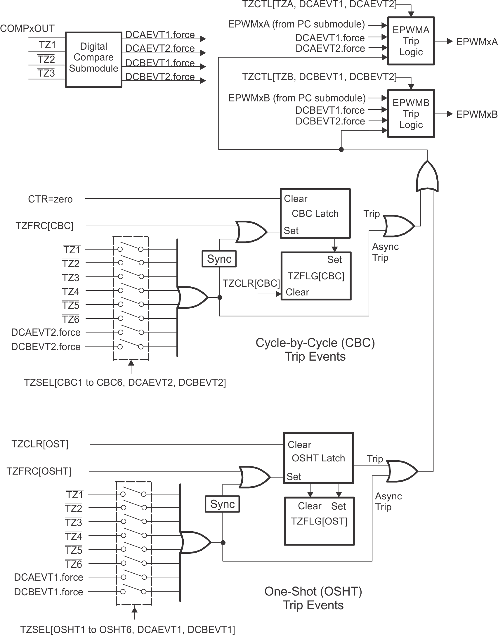
I'm using the TMS320F32031. I have setup ePWM1 with EPWM1A set at 0 and clear at CMPA. I have setup EPWM1B to clear at 0 and clear at CMPA. This works fine. I have also setup the DC submodule, using the comparator, to feed into the trip zone submodule (CBC trip, DCAEVT2, DCBEVT2). This also appears to be working fine. My problem is physical output of EPWM1A and EPWM1B when probing with an oscilloscope. I believe I can see the CBC trip, trying to occur, but it's not actually occurring. EPWM1A, which is set to force low, appears to "float" low when the CBC trip occurs. EPWM1B, which is set to force high, also appears to "float" when the CBC trip occurs, but the signal does not ever go high. When no CBC trip occurs, the signals look perfect. Both signals behave as commanded when the counter reaches 0 and CMPA. Below is a copy of my setup. I originally wanted to use the DB submodule of the peripheral to control the outputs, but I thought that was interfering with the CBC sub module. I tried using a DCxEVT2 sync signal and async signal, filtered and unfiltered. I also tried using DCBHCOMPSEL vs. DCBLCOMPSEL. What am I doing incorrectly? I have pasted portions of my code below. Note n = pwm = 1, master = 1, invert = 0, period = 60, phase = 2.
// Time Base SubModule Registers
(*ePWM[n]).TBCTL.bit.PRDLD = TB_IMMEDIATE; // set Immediate load
(*ePWM[n]).TBPRD = period-1; // PWM frequency = 1 / period
(*ePWM[n]).TBPHS.half.TBPHS = 0;
//(*ePWM[n]).TBCTR = 0;
(*ePWM[n]).TBCTL.bit.CTRMODE = TB_COUNT_UP;
(*ePWM[n]).TBCTL.bit.HSPCLKDIV = TB_DIV1;
(*ePWM[n]).TBCTL.bit.CLKDIV = TB_DIV1;
if(mode == 1) {// config as a Master
(*ePWM[n]).TBCTL.bit.PHSEN = TB_DISABLE;
(*ePWM[n]).TBCTL.bit.SYNCOSEL = TB_CTR_ZERO; // sync "down-stream"
}
else if(mode == 0) { // config as a Slave (Note: Phase+2 value used to compensate for logic delay)
(*ePWM[n]).TBCTL.bit.PHSEN = TB_ENABLE;
(*ePWM[n]).TBCTL.bit.SYNCOSEL = TB_SYNC_IN;
if ((0 <= phase)&&(phase <= 2)) (*ePWM[n]).TBPHS.half.TBPHS = (2-phase);
else if (phase > 2) (*ePWM[n]).TBPHS.half.TBPHS = (period-phase+2);
}
// Counter Compare Submodule Registers
(*ePWM[n]).CMPA.half.CMPA = 0; // set duty 0% initially
(*ePWM[n]).CMPCTL.bit.SHDWAMODE = CC_SHADOW;
(*ePWM[n]).CMPCTL.bit.LOADAMODE = CC_CTR_PRD;
(*ePWM[n]).CMPB = 0; // set duty 0% initially
(*ePWM[n]).CMPCTL.bit.SHDWBMODE = CC_SHADOW;
(*ePWM[n]).CMPCTL.bit.LOADBMODE = CC_CTR_PRD;
// Action Qualifier SubModule Registers
if (invert) {
(*ePWM[n]).AQCTLA.bit.ZRO = AQ_CLEAR;
(*ePWM[n]).AQCTLA.bit.CAU = AQ_SET;
(*ePWM[n]).AQCTLB.bit.ZRO = AQ_SET;
(*ePWM[n]).AQCTLB.bit.CAU = AQ_CLEAR;
}
else {
(*ePWM[n]).AQCTLA.bit.ZRO = AQ_SET;
(*ePWM[n]).AQCTLA.bit.CAU = AQ_CLEAR;
(*ePWM[n]).AQCTLB.bit.ZRO = AQ_CLEAR;
(*ePWM[n]).AQCTLB.bit.CAU = AQ_SET;
}
ePWM[pwm]->TBCTL.bit.FREE_SOFT = 3;
//SETUP DIGITAL COMPARE FOR CURRENT
if (ps->parameters.bits.feedbackPin == 2) {
ePWM[pwm]->DCTRIPSEL.bit.DCAHCOMPSEL = 8; //COMP 1 OUT
ePWM[pwm]->DCTRIPSEL.bit.DCBHCOMPSEL = 8; //COMP 1 OUT
}
else if (ps->parameters.bits.feedbackPin == 4) {
ePWM[pwm]->DCTRIPSEL.bit.DCAHCOMPSEL = 9; //COMP 2 OUT
ePWM[pwm]->DCTRIPSEL.bit.DCBHCOMPSEL = 9; //COMP 2 OUT
}
ePWM[pwm]->DCACTL.bit.EVT2FRCSYNCSEL = 1; //async signal
ePWM[pwm]->DCACTL.bit.EVT2SRCSEL = 0; //filtered signal
ePWM[pwm]->DCBCTL.bit.EVT2FRCSYNCSEL = 1; //async signal
ePWM[pwm]->DCBCTL.bit.EVT2SRCSEL = 0; //filtered signal
ePWM[pwm]->DCFCTL.bit.PULSESEL = 1; //time base counter equal to 0
ePWM[pwm]->DCFCTL.bit.BLANKINV = 0; //blanking window not inverted
ePWM[pwm]->DCFCTL.bit.SRCSEL = 1; //DCAEVT2 is source signal (equivalent to DCBEVT2)
ePWM[pwm]->DCCAPCTL.bit.CAPE = 0; //enable the time-base counter capture
ePWM[pwm]->DCFOFFSET = 0;
ePWM[pwm]->DCFWINDOW = RISING_EDGE_DELAY + 1; //dead band time + time for load cap to discharge (1 * 16.7ns should be plenty)!!
ePWM[pwm]->DCFCTL.bit.BLANKE = 0; //blanking window is enabled
//SETUP TRIP ZONE FOR CURRENT CBC TRIP
ePWM[pwm]->TZSEL.bit.DCAEVT2 = 1; //CBC trip from DCAEVT2
ePWM[pwm]->TZSEL.bit.DCBEVT2 = 1; //CBC trip from DCBEVT2
ePWM[pwm]->TZDCSEL.bit.DCBEVT2 = 2; //DCBL = don't care, DCBH = high
ePWM[pwm]->TZDCSEL.bit.DCAEVT2 = 2; //DCAL = don't care, DCAH = high
if (invert) {
ePWM[pwm]->TZCTL.bit.DCBEVT2 = 2; //force B low (low side off)
ePWM[pwm]->TZCTL.bit.DCAEVT2 = 1; //force A high (high side on)
}
else {
ePWM[pwm]->TZCTL.bit.DCBEVT2 = 1; //force B high (low side on)
ePWM[pwm]->TZCTL.bit.DCAEVT2 = 2; //force A low (high side off)
}

