


Hello,
I am experiencing a perplexing problem with the TMS320F28335. I am using it to control an LLC resonant converter, where my sensors are monitoring DC values. I am running the system in open loop, so said sensors are only monitoring and not controlling the system. At seemingly random, the DSP will calculate a suddenly large value for a single computation cycle while no such fluctuation occurs at the corresponding input pin.
Measurement setup:
Isolated scope-corder with 100MS/s isolated channels
Measuring voltage at the ADC input pin with CH1
Using an ePWM port at 200kHz and measured through 10KHz low-pass hardware filter to create real time digital-to-analog (D2A) output - CH2
Software protection shuts the system down if the ADC result passes an internal threshold
Observing the first scope capture below, you can see that when the spike is observed on CH2 (D2A), CH1 (ADC pin) shows unusual fluctuation at all. CH2's output becomes notably less noisy after the the spike because hardware protection is triggered at that moment, indicating the value from the ADC result buffer is being represented by the D2A output (as opposed to an issue with ePWM module/code). I would have suspected the acquisition window was not wide enough, but I would expect that to generate a low value rather than an extremely large one, since the sensing capacitor would not be insufficiently charged in that case. Indeed, increasing the ADC acquisition window did not have any noticeable effect. I have monitored the execution time of the ADC as well, and the sequence is completed well before the next iteration.
To make matters more interesting, there is another F28335 on the control board controlling a previous stage of the system, which is NOT experiencing this issue, that has identical hardware configuration, System clock configuration, High-speed clock configuration, and ADC configuration (aside from different different number of pins and the SOC is generated from the timer0 ISR rather than the ePWM module). There is also a parallel project in our lab with a near identical control board that is experiencing this issue on BOTH DSPs on three separate boards. We are mistakenly using a 1.8V core voltage while running at 150MHz rather than the proper 1.9V, but many previous projects in our lab have done so without experiencing a similar issue. Furthermore, both projects are using DSPs with different batch numbers.
I have been on the phone with a TI representative who attempted to find a related forum in addition to my own searching, but with no luck. Any assistance would be immensely appreciated!!!
If possible, I would also very much appreciate a phone conversation with your engineers or opening a private email thread with them for additional debugging of this problem.
Scope Captures:
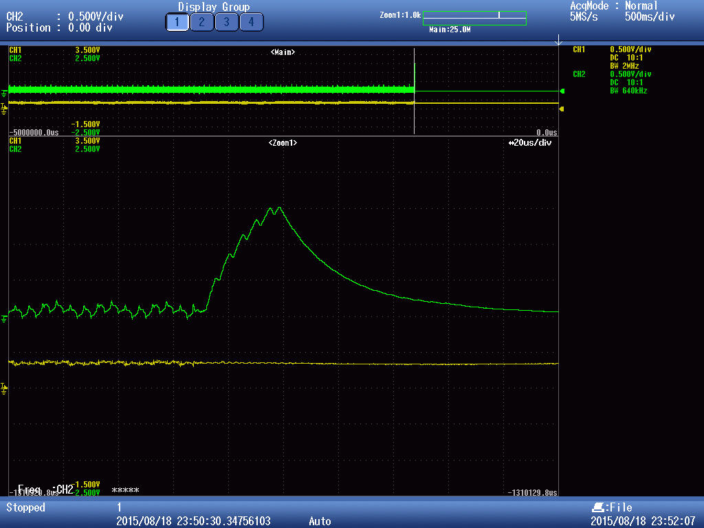
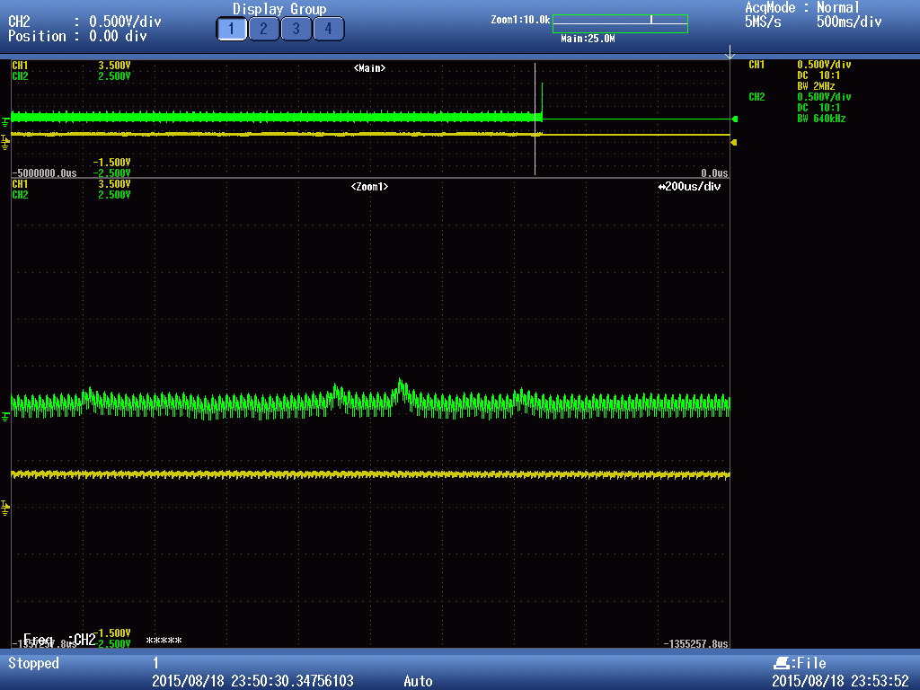
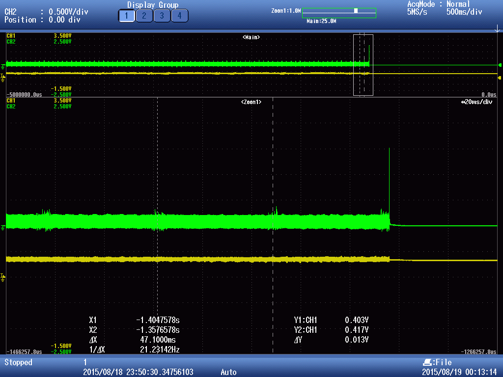
The errors are not always large, and, on a smaller scale, clusters of the errors appear to be periodic, but at a much lower frequency than any switching in my system (see 2 captures below: 1st close-up, 2nd frequency):
Hardware Configuration:
DSP Part #: TMS320F28335PGFA
DSP Batch #: CA - 44A4GCW G4
Core voltage: 1.8V
External oscillator: 30MHz

Software Configuration Settings:
//=========================================================================================================================
// SYSTEM CLOCK and timer0 Configuration
#define CPU_FRQ_150MHZ 1 // This definition is used in several of the initialization functions indicating 150MHz clock
#define CPU_RATE 6.667L // for a 150MHz CPU clock speed (SYSCLKOUT)
#define SYSCLK_DIVSEL 2 // Oscillator frequency multiplier: 1-10, 0 = bypass (PFC Oscillator = 30MHz)
#define SYSCLK_DIV 10 // Oscillator frequency divider: 0, 1 = OSCCLK/4, 2 = OSCCLK/2, 3 = OSCCLK/1
// CPUTIMER INERUPT TIMER VALUE
#define Tmr0Period 30e-6 // Period of high-speed loop calculation in seconds = 33.33333kHz
//=========================================================================================================================
// HIGH SPEED CLOCK
SysCtrlRegs.HISPCP.bit.HSPCLK = 1; // HISPCP only has one 3-bit field, 0: HSPCLK = SYSCLKOUT, 1-7: HSPCLK = SYSCLKOUT/(2*HISPCP[HSPCLK])
//=========================================================================================================================
// ADC Module Configuration
void ADC_Config(void)
{
// STEP1: Call InitADC function
InitAdc();
EALLOW; // ADC Registers are EALLOW protected
// STEP2: ADC CLOCK
// From System_Config: HSPCLK = SYSCLKOUT/2 = 75MHz
// See TMS320x2833x, Analogue-to-Digital Converter (ADC) Module, pp.34-35, pp.37-38.
AdcRegs.ADCTRL3.bit.ADCCLKPS = 3; // Core Clock Divider = 4 bit value >> 0: F_clk = HSPCLK, 1-15: F_clk = HSPCLK/(2*ADCCLKPS[3:0])
AdcRegs.ADCTRL1.bit.CPS = 1; // 1: ADCCLK = F_clk/2
// STEP3: ADC Control 1 Register (ADCTRL1)
// See TMS320x2833x, Analogue-to-Digital Converter (ADC) Module, pp.34-35.
AdcRegs.ADCTRL1.bit.SEQ_CASC = 1; // 1 = Cascaded Mode: SEQ
AdcRegs.ADCTRL1.bit.SEQ_OVRD = 0; // 0 = Sequencer Override disabled - wraparound on MAX_CONVn,
AdcRegs.ADCTRL1.bit.CONT_RUN = 0; // 0 = Start-Stop mode - Stop on EOS, reset from software,
AdcRegs.ADCTRL1.bit.ACQ_PS = 10; // 4-bit field: Aquisition Time Window = (ADCTRL1[11:8] + 1) * ADCCLK Period
AdcRegs.ADCTRL1.bit.SUSMOD = 3; // 3 = stop immediately
// STEP4: ADC Control 2 Register (ADCTRL2)
// See TMS320x2833x, Analogue-to-Digital Converter (ADC) Module, pp.35-36.
AdcRegs.ADCTRL2.bit.EPWM_SOCB_SEQ2 = 1; // 1 = ePWMx SOCB trigger for SEQ2 ENABLED
AdcRegs.ADCTRL2.bit.INT_MOD_SEQ2 = 0; // 0 = INT_SEQ2 set every end of SEQ2,
AdcRegs.ADCTRL2.bit.INT_ENA_SEQ2 = 0; // 0 = Interrupt request by INT_SEQ2 DISABLED,
AdcRegs.ADCTRL2.bit.EXT_SOC_SEQ1 = 0; // 0 = no effect,
AdcRegs.ADCTRL2.bit.EPWM_SOCA_SEQ1 = 1; // 1 = ePWMx SOCA trigger for SEQ1 ENABLED
AdcRegs.ADCTRL2.bit.INT_MOD_SEQ1 = 0; // 0 = INT_SEQ1 set every end of SEQ1,
AdcRegs.ADCTRL2.bit.INT_ENA_SEQ1 = 1; // 1 = Interrupt request by INT_SEQ1 ENABLED
AdcRegs.ADCTRL2.bit.EPWM_SOCB_SEQ = 0; // 0 = No action,
// STEP5: ADC Control 3 Register (ADCTRL3)
// See TMS320x2833x, Analogue-to-Digital Converter (ADC) Module, pp.37-38.
AdcRegs.ADCTRL3.bit.SMODE_SEL = 0; // 0 = Sequential Sampling selected,
// STEP6: ADC Maximum Conversion Channels Register (ADCMAXCONV)
// See TMS320x2833x, Analogue-to-Digital Converter (ADC) Module, pp.38-39.
AdcRegs.ADCMAXCONV.bit.MAX_CONV1 = ADC_CONV; // 4-bit value (0 to15) = 1 to 16 Conversions
AdcRegs.ADCMAXCONV.bit.MAX_CONV2 = 0; // 3-bit value (0 to 7) = 1 to 8 Conversions - ignored in Cascaded sequencer mode
// STEP7.1: ADC Input Channel Select Sequencing Control 1 Registers (ADCCHSELSEQ1)
// See TMS320x2833x, Analogue-to-Digital Converter (ADC) Module, pp.44-45.
AdcRegs.ADCCHSELSEQ1.all = 0x3210; // Select Sequencer A lower: ADCINA0, ADCINA1, ADCINA2, ADCINA3
// STEP7.2: ADC Input Channel Select Sequencing Control 2 Registers (ADCCHSELSEQ2)
// See TMS320x2833x, Analogue-to-Digital Converter (ADC) Module, pp.44-45.
AdcRegs.ADCCHSELSEQ2.all = 0x7654; // Select Sequencer A Upper: ADCINA4, ADCINA5, ADCINA6, ADCINA7
// STEP7.3: ADC Input Channel Select Sequencing Control 3 Registers (ADCCHSELSEQ3)
// See TMS320x2833x, Analogue-to-Digital Converter (ADC) Module, pp.44-45.
AdcRegs.ADCCHSELSEQ3.all = 0xBA98; // Select Sequencer B lower: ADCINB0, ADCINB1, ADCINB2, ADCINB3
// STEP7.4: ADC Input Channel Select Sequencing Control 4 Registers (ADCCHSELSEQ4)
// See TMS320x2833x, Analogue-to-Digital Converter (ADC) Module, pp.44-45.
AdcRegs.ADCCHSELSEQ4.all = 0xFEDC; // Select Sequencer B Upper: ADCINB4, ADCINB5, ADCINB6, ADCINB7
// STEP8: ADC Status and Flag Register (ADCST)
// See TMS320x2833x, Analogue-to-Digital Converter (ADC) Module, p.41 & pp. 35-36.
AdcRegs.ADCST.bit.INT_SEQ1_CLR = 1; // 1 = Clears SEQ1 interrupt flag bit, INT_SEQ1
AdcRegs.ADCST.bit.INT_SEQ2_CLR = 1; // 1 = Clears SEQ2 interrupt flag bit, INT_SEQ2
AdcRegs.ADCTRL2.bit.RST_SEQ1 = 1; // 1 = Imediately resset Sequencer 1 to state CONV00 - abort active conversion
AdcRegs.ADCTRL2.bit.RST_SEQ2 = 1; // 1 = Imediately resset Sequencer 2 to pretriggered state - i.e. waiting at CONV08 - abort active conversion
EDIS;
}
void InitAdc(void)
{
extern void DSP28x_usDelay(Uint32 Count);
EALLOW;
SysCtrlRegs.PCLKCR0.bit.ADCENCLK = 1; //Ensure ADC clock is enabled
AdcRegs.ADCREFSEL.bit.REF_SEL = 0; //Select internal BG reference
ADC_cal(); //Copies ADC calibration values from TI OTP to ADCREFSEL & ADCOFFTRIM
EDIS;
AdcRegs.ADCTRL3.all = 0x00E0; // Power up bandgap/reference/ADC circuits
DELAY_US(ADC_usDELAY); // Delay before converting ADC channels
}
//=========================================================================================================================
// How SOC is triggered at the start of timer0 ISR
DCDC_ADC.Poll(&DCDC_ADC); // Please see function below
AdcRegs.ADCTRL2.bit.RST_SEQ1 = 1; // When using software SOC, the sequencers must be reset by software as well
AdcRegs.ADCTRL2.bit.RST_SEQ2 = 1;
AdcRegs.ADCTRL2.bit.SOC_SEQ1 = 1; // Trigger SOC to start conversion of measurements for next computation cycle
IER &= 0xC007; // Disable all CPU Interrupts except Real-time OS, Data log, PIE group 1 & current PIE group 3,
IER |= 0x0006; // Ensure PIE group 2 (EPWM1 TZ) is enable (has higher priority)
PieCtrlRegs.PIEACK.all = 0xFFFF; // ACK all PIE interrupts & llow PIE module to send new interrupts from all groups
asm(" RPT #5 || NOP"); // Wait x cycles: this will flush pipeline
EINT; // Global interrupt mask ENABLE
DCDC_ADC.Calc(&DCDC_ADC); // Please see function below
//=========================================================================================================================
// ADC Results polling and conversion functions
void ADCValue_Poll (ADCVALUE *v)
{ int i;
// Read the adc results into the raw data array
for(i=0;i <= ADC_CONV;i++) {v->ADCValue.all[i] = *(&AdcMirror.ADCRESULT0+i);}
GpioDataRegs.GPACLEAR.bit.GPIO13 = 1;
}
void ADCValue_Calc (ADCVALUE *v)
{ int i;
// Convert raw ADC values to real world values as RW = (Raw*Gain)+Offset
for(i=0;i <= ADC_CONV;i++) {v->RWValue.all[i] = (v->ADCValue.all[i] * v->Gain.all[i]) + v->OffSet.all[i];}
GpioDataRegs.GPACLEAR.bit.GPIO14 = 1;
}


