


Hello,
we have two code like in figure one for sci and other for adc
how can initialize different module available in C2000 Family ???
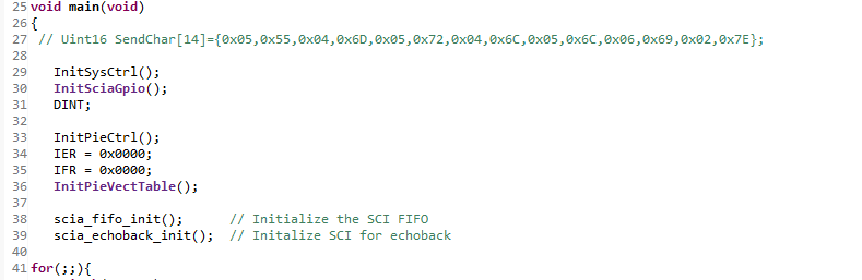
CODE FOR SCI
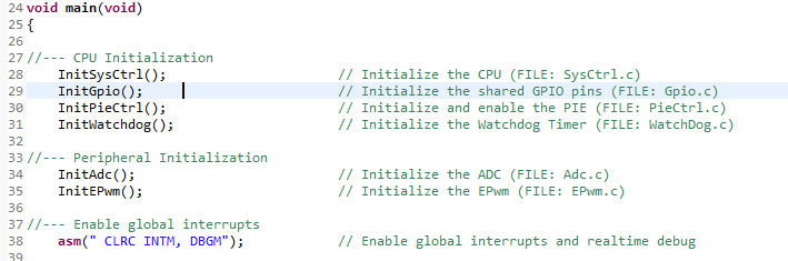
CODE FOR ADC
Hello,
we have two code like in figure one for sci and other for adc
how can initialize different module available in C2000 Family ???
CODE FOR SCI
CODE FOR ADC

