This thread has been locked.

If you have a related question, please click the "Ask a related question" button in the top right corner. The newly created question will be automatically linked to this question.

Problem with external reference for ADC (TMS320F280x)

Other Parts Discussed in Thread: TMS320F2808

Hello!

We are using a TMS320F2808 and trying to measure a given signal (~1.2V) with different references. Whenever we calculate the measured voltage we see that we always use 3.0V as reference.

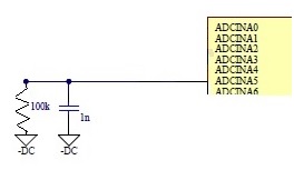
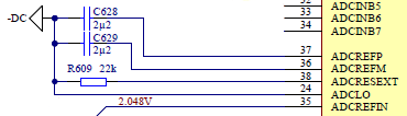
Our connection is as follows:

And code:    
DELAY_US(10000L); AdcRegs.ADCTRL1.bit.RESET = 1; DELAY_US(ADC_usDELAY); asm(" NOP "); asm(" NOP "); AdcRegs.ADCREFSEL.bit.REF_SEL = 0x1; DELAY_US(ADC_usDELAY); // Acquisition window size. This bit field controls the width of SOC pulse, which, in turn, // determines for what time duration the sampling switch is closed. AdcRegs.ADCTRL1.bit.ACQ_PS = 0x0; // Core clock prescaler. The prescaler is applied to divided device peripheral clock, HSPCLK (High Speed Prescaler Clock). AdcRegs.ADCTRL1.bit.CPS = 0x1; // Continuous run AdcRegs.ADCTRL1.bit.CONT_RUN = 0x1; // Setup sequencer AdcRegs.ADCCHSELSEQ1.bit.CONV00 = 0x8; DELAY_US(ADC_usDELAY); // Start ADC AdcRegs.ADCTRL3.all = ADC_POWER_UP; DELAY_US(ADC_usDELAY); // Start conversion AdcRegs.ADCTRL2.bit.SOC_SEQ1 = 0x1;

Where ADC_usDELAY = 10ms and we enable the ADC module clock in another module.

If i measure 1.13V on ADCINB0 (according to datasheet 0x8 in AdcRegs.ADCCHSELSEQ1.bit.CONV00 gives me the converted result from ADCINB0 in ADCRESULT0) I expect the value 1.13 / 2.048 * 4096 = 2260 in the result register. Though I get the value 1542, which corresponds to a reference of 3.0V (internal bandgap reference).

Is there something wrong with the software or is the hardware connection wrong?

I tried to search but haven't seen any similar problem.

Thanks in advance!

  • Hi Golgor,

    Everything is working exactly as it should.  The F2808 ADC full scale voltage is always 3.0V regardless of what reference mode is selected.  The purpose of external reference mode is so that a more accurate reference can be used to reduce the gain error.  Multiple options are provided in common reference voltages for convenience, but the full scale voltage does not ratiometrically scale with the reference voltage.

    Regards,

    Joe

  • Thanks for the answer,

    Though, how do I make use of a more stable reference? Is this done internally and nothing I can see? i.e. it uses the choosen reference to balance the 3.0V bandgap "behind the scenes"?
  • The ADC user guide details how to configure the device for internal vs. external reference mode.  We specify different gain error limits in the datasheet (ADC Electrical Characteristics) depending on internal vs. external reference with external reference being better.  Of course you have to account for any error introduced by your external reference.

    In the device the reference voltage and ADC input voltage are scaled to matching ranges depending on the mode selected.  The ADC result registers will always give you something around 0 for an input of 0V and something around 4095 for an input voltage of 3V regardless of the reference mode.  I say "something around" since you have to account for offset, gain, and linearity error as well as noise.

    If I have missed your question, please clarify.

    Regards,

    Joe

  • Hello Joe,

    I'm aware of the ADC user guide. The problem we are struggling with is that we need a high precision conversion and recent examples of the DSP we use changed in their behavior. There is no good explanation on how the external reference is used and what it really does. Me and several other engineers, after reading the ADC Guide, was led to believe the external reference would affect the ADCRESULT.

    "By default, an internally generated bandgap voltage reference is selected to supply the ADC logic. Based on customer application requirements, the ADC logic may be supplied by an external voltage reference."

    That's basically everything that it says about external references. The rest of the text is just describing how to connect the hardware etc.

    Also I have been reading in "TMS320280x and TMS3202801x ADC Calibration" (SPRAAD8A) about ADC calibration and this guide doesn't even mention the external reference and if external references in any way influences the calibration.

    I will look into the SPRAAD8A and try to get calibration code running and see if we can improve our measurements.

  • Golgor,

    I apologize for any confusion.  I realize now that unlike most C2000 devices, the F280x family has the same gain error spec for internal and external reference mode.  Typically we can say that better performance will be achieved using an external reference and the data sheet usually reflects that in the gain error spec, but not in this case.  In fact from a spec perspective there is no benefit to using an external reference.  It might be true that from a practical perspective you may get better performance with external reference, but we will not be able to guarantee performance better than that specified in the DS.

    Usually we are able to separate the gain error into two sources, one from the converter itself and the other from the internal bandgap voltage.  In those cases we will specify the gain error for external reference mode as the  error due only to the converter and leave it to the customer to consider what additional error should be factored from their external reference design.  In this case, most likely due to production test limitations, we are not able to spec better performance with external reference.

    At this point your best bet probably is with using the calibration technique you referenced in the post.


    Regards,

    Joe

  • Golgor, I should make another recommendation. I know there are many reasons behind device selection, but from the perspective of ADC accuracy, there are a couple other device options that may suit you better. F2833x has a similar ADC architecture and throughput as F280x but half the gain error (incidentally this is another device with the same spec for internal and external reference range). We also have a newer device family F2807x (search F28075) which only has external reference mode but gain error is spec'd at +/-5LSB and offset error +/-4LSB.
  • Thanks for the answer Joe,

    The F2808 is used in a product that is about the be phased out in a couple of years and I seriously doubt there will be resources for changing DSP. Though, it was good to hear that there is no guaranteed difference between the external and internal reference. We noticed it but almost thought it must be typo, because it didn't fit into the idea we had about how the ADC works.

    I will look into the ADC Calibration document and try to find a solution. Hardware-wise it is possible to use two ADC-channels for correcting the ADC measurements.

    We are just curious, what does the external reference do in this device, do you know?

    Thanks for your answers!

    Robert

  • Hi TI

    Below is a part of the circuit, including the TMS320F2808, that Golgor and I are working on. Depending on which ADCINA pin we connect the resistor and capacitor to, we measure between 17 mV and 27 mV across the resistor. Why is the voltage across the resistor different from 0 V? What causes this leakage current through the resistor and can you elaborate on this leakage current's characteristics?

    Vcc = -DC 

    If we set the ADCOFFTRIM to an offset value, will the automatic gain error correction (GEC) calculation based on an external reference be redone so that we get an error correction like this y = GEC*x+ADCOFFTRIM?

  • Hi TI,

    Not having read much of the document I want to try and raise a few thoughts that I believe that you might be able to answer rather easily - and I guess that rather soon would be much appreciated:

    Is there any way to make an offset trim without using the regular ADC inputs (but instead to use VSSA2) and what drawbacks would you expect considering the possibility that the offset might be negative?

    Does the leakage current on the ADC input mean that the generator impedance of the signal source must be low enough as to avoid or reduce impact from this leakage current?

    BR

    Andy
  • Golgor said:

    The F2808 is used in a product that is about the be phased out in a couple of years and I seriously doubt there will be resources for changing DSP.

    Understood, hopefully F280x will work for this application as well.

    Golgor said:

    We are just curious, what does the external reference do in this device, do you know?

    Using external reference has the same function as using the internal bandgap, namely to provide a reference voltage which the ADC input is compared against to determine the digital code.  Sometime the bandgap can contribute a significant amount of error to the reference voltage, in particular temperature drift.  In the case of F280x we see the error due to the buffer after the mux and/or in the converter itself >> than that of the band gap, therefore selecting the external reference option doesn't offer an improvement.  Note, the below picture is conceptual and does not necessarily reflect the actual implementation/architecture.

    user4531652 said:


      Is there any way to make an offset trim without using the regular ADC inputs (but instead to use VSSA2) and what drawbacks would you expect considering the possibility that the offset might be negative?

    Some other C2000 devices have an internal connection to REFLO or VSSA allowing them to be sampled without sacrificing an ADC input, but I'm afraid that is not the case for F280x.


    user4531652 said:

    Does the leakage current on the ADC input mean that the generator impedance of the signal source must be low enough as to avoid or reduce impact from this leakage current?

    Yes, but in addition to leakage, there will be active current as the internal S/H cap charges during sampling.  You may have to increase the sample and hold time to let the cap fully charge.  Note the below input model is not from F280x documentation but the principle is the same.

    Regards,

    Joe

  • Hi TI,

    Many thanks for the rapid answer and the explanations.

    I browsed through some of the documents referred to and came to some conclusions:

    There is an analog gain adjustment to accommodate for different external VREF:s and as said in SPRAAD8A (quoted below) one would also draw the conclusion that the offset adjustment is analog. This would mean that a negative offset won’t stop us from measuring down to 0V (ADCLO) and that given adequate offset correction, the ADC would in fact enable measurement of voltage levels slightly lower than 0V (ADCLO). This is good news and the procedure for offset error correction described in the Reference Guide (1.9) could be used to ensure that the full input range (down to 0V) can be measured.

    “The value in this register changes the analog characteristics of the ADC, allowing full offset compensation while maintaining the native range of the ADC.

    Referring to SPRAAD8A, I think I can draw the conclusion that with the above mentioned procedure, the worst case offset error can be reduced, although not completely as there are factors that can be generally compensated for (such as e.g. temperature drift).

    Is it by the way correctly understood that the temperature variation has a positive coefficient of 50ppm/C (as described in SPRAAD8A - 8 Gain and Offset Temperature Drift)?

    When it comes to gain calibration (described SPRAAD8A) I draw the conclusion that the gain correction is digital and therefore has to be calculated after the ADC conversion, at least I can’t find any register from where this could be controlled. Is this correctly understood (I only browsed through the documents)?

    Thank you for your kind assistance,

    Andy

  • Hi TI,

    If we set the ADCOFFTRIM to an offset value, will the automatic gain error correction (GEC) calculation based on an external reference be redone so that we get an error correction like this y = GEC*x+ADCOFFTRIM?

  • I note that although the inaccuracy in the buffer stage is much worse than that of the internal reference, the reason to choose an external reference might be that one can improve temperature drift.

    I also wonder if you could explain why it would be safe choosing 15LSB for an offset value whereas the maximum offset is 60LSB as I understand it.
  • user4531652 said:

    There is an analog gain adjustment to accommodate for different external VREF:s and as said in SPRAAD8A (quoted below) one would also draw the conclusion that the offset adjustment is analog. This would mean that a negative offset won’t stop us from measuring down to 0V (ADCLO) and that given adequate offset correction, the ADC would in fact enable measurement of voltage levels slightly lower than 0V (ADCLO). This is good news and the procedure for offset error correction described in the Reference Guide (1.9) could be used to ensure that the full input range (down to 0V) can be measured.

    “The value in this register changes the analog characteristics of the ADC, allowing full offset compensation while maintaining the native range of the ADC.

    Correct, the offset trim is implemented in the analog domain and you can measure and calibrate for negative offset.

    user4531652 said:

    Referring to SPRAAD8A, I think I can draw the conclusion that with the above mentioned procedure, the worst case offset error can be reduced, although not completely as there are factors that can be generally compensated for (such as e.g. temperature drift).

    Is it by the way correctly understood that the temperature variation has a positive coefficient of 50ppm/C (as described in SPRAAD8A - 8 Gain and Offset Temperature Drift)?

    The app note certainly implies the temp coefficient it always positive and generally speaking that is true, however it is not guaranteed by test.  In fact, based on a very gross analysis of production data, it appears it can be negative. 

    user4531652 said:

    When it comes to gain calibration (described SPRAAD8A) I draw the conclusion that the gain correction is digital and therefore has to be calculated after the ADC conversion, at least I can’t find any register from where this could be controlled. Is this correctly understood (I only browsed through the documents)?

    You are correct, the gain error calibration described in that app note is really software compensation of the ADC conversion results, in other words in the digital domain as you say, but I should also point out it will introduce additional latency to when the conversion results are available if that is a care about.

    Fredrik Olin said:

    If we set the ADCOFFTRIM to an offset value, will the automatic gain error correction (GEC) calculation based on an external reference be redone so that we get an error correction like this y = GEC*x+ADCOFFTRIM?

    Yes, if you are sampling ADCLO to calibrate the offset error, this should be done before calibrating the gain error, since gain and offset error cannot be separated when sampling a single voltage not near ADCLO (i.e. during the gain calibration).  For example if you force 2.5V and the conversion result is 10LSB from ideal, you cannot tell how much is offset and how much is gain without first calibrating out the offset error.  If I may, I would also advise (as a one time experiment during delevopment) examining maybe 100 conversions of ADCLO to see if there is any ringing on the signal from the initial closing of the S/H cap.  This has been observed in some situations and can lead to a false OFFSET trim.  If the conversions are stable, then there is no problem, but if you see ringing, you may have to take an average of the conversions after the ringing has settled.

    Also I said "if you are sampling ADCLO" because I have also seen gain/offset calibration done by forcing two non-zero voltages (i.e. 0.6V and 2.4V) and using those two points to linearly extrapolate the gain and offset (gain is just the slope, offset is the y-intercept).  In this case, both are effectively calculated at the same time.

    Fredrik Olin said:
    I note that although the inaccuracy in the buffer stage is much worse than that of the internal reference, the reason to choose an external reference might be that one can improve temperature drift.

    Sure using external reference is perfectly fine.  The datasheet does not guarantee better performance, but certainly it is logical to believe you might get better performance. 

    Fredrik Olin said:
    I also wonder if you could explain why it would be safe choosing 15LSB for an offset value whereas the maximum offset is 60LSB as I understand it.

    Good point, there is no reason you can't bump the trim register by 60 or more.  The register itself supports -256 to +255.
    Regards,
    Joe