According to the technical reference manual(spruhm8e), there are 2 IO options for SCIBoot mode as shown below:
Is this chosen of options determined by the user? If is, how to configure?
This thread has been locked.
If you have a related question, please click the "Ask a related question" button in the top right corner. The newly created question will be automatically linked to this question.
Hi,
Is this chosen of options determined by the user?
Yes, it's determined by user.
If is, how to configure?
This is done by configuring the Zx-BOOTCTRL location in USER OTP. This location is part of security setting in USER OTP and can be programmed independently using CCS flash plug-in or by flash API. Please note that since this location is in OTP and ECC enabled, it can be programmed only once so user has to be very careful while programming this. If incorrect value get programmed then value can not be changed and user may have to replace the part.
Please refer "Table 3-4. BOOTCTRL Register Bit Definition for CPU1" and "Table 3-6. Get Mode Decoding on CPU1" in TRM for definition of this register location.
Regards,
Vivek Singh
Hi, Vivek
My understanding is that the Zx-BOOTCTRL configuration only changes the boot mode pins which are GPIO84 and GPIO72 as default setting. In other words, OPT_BOOTPIN0 picks the boot mode pin 0, and OPT_BOOTPIN1 picks the boot mode pin 1.
My question is how to configure the SCI BOOT pins as there are two options(option 1 with GPIO84 and GPIO85, option2 with GPIO28 and GPIO29). I noticed that there are also two SCI BOOT mode In Table 3-6. Get Mode Decoding on CPU1 named SCI BOOT0 and SCI BOOT1. Is SCIBoot IO Option 1 corresponding to SCI BOOT 0 and SCIBoot IO Option 2 corresponding to SCI BOOT 1?
Thanks!
Hi,
Is SCIBoot IO Option 1 corresponding to SCI BOOT 0 and SCIBoot IO Option 2 corresponding to SCI BOOT 1?
Yes, that's correct. We'll try to update the document to have same name at both the places to avoid this confusion.
Regards,
Vivek Singh
Vesgine,
1) SCI BOOTPIN0 option: SCITX (GPIO84) & SCIRX (GPIO85)
2) Follow the below steps to configure SCI boot in CPU2
a) CPU2 boot rom on startup initializes CPU2 sub system, performs RAM initialization as per RESC, installs PIE interrupt handler to serve IPC commands from CPU1 and goes into IDLE mode.
b) CPU1 application code should be configure GPIOs as SCI pins
c) CPU1 application code should set IPCBOOTMODE = 1 (SCI boot mode)
d) CPU1 application code should set IPCSENDCOM = 19 (This IPC command commands CPU2 to execute bootloader as requested by
C1TOC2BOOTMODE register)
Regards,
Manoj
Hi, Manoj
According to CPU2 Flow chart as shown below, if ZxBOOTCTRL.OTP_KEY==0x5A and ZxBOOTCTRL.OTP_BMODE == FLASH_BOOT, then CPU2 will enter FLASH BOOT mode but not WAIT BOOT mode. In this case, SCI boot is not implemented. As ZxBOOTCTRL register is programmed only once, this means CPU2 will always branch to FLASH BOOT or WAIT BOOT mode, and switching between this two boot modes is not allowed.
For normal operation, CPU2 boots from FLASH. When CPU2 needs to be reprogrammed by FLASH programming tool(like C2Prog), CPU2 should boot from SCI.
So how to implement this requirement?
Hi,
I have noticed that each CPU has its own ZxBOOTCTRL registers. But the question I mentioned above is focusing on CPU2. Let's make it clearly. "According to CPU2 Flow chart, if ZxBOOTCTRL.OTP_KEY of CPU2 ==0x5A and ZxBOOTCTRL.OTP_BMODE of CPU2 == FLASH_BOOT, then CPU2 will enter FLASH BOOT mode but not WAIT BOOT mode. In this case, SCI boot is not implemented. As ZxBOOTCTRL register of CPU2 is programmed only once, this means CPU2 will always branch to FLASH BOOT or WAIT BOOT mode, and switching between this two boot modes is not allowed."
Hi,
Question 1:
For new devices, the factory value of Zx-BOOTCTRL registers are 0xFFFFFFFF. According to the CPU2 flow chart, CPU2 will enter WAIT BOOT mode(because Zx-BOOTCTRL.OTP_KEY != 0x5A). If the CPU1 application doesn't send any boot command to CPU2 by IPC, does that mean CPU2 will never startup?
Question 2:
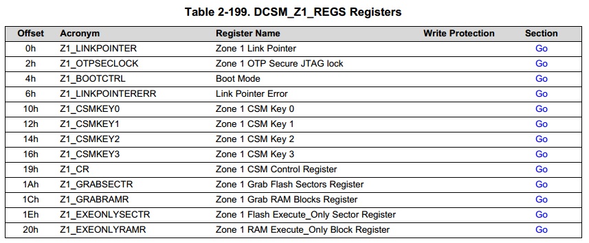
There are two kinds of registers namely DCSM_Z1_OTP and DCSM_Z1_REGS as shown below.
Is Z1_BOOTCTRL register memory-mapped of Z1OPT_BOOTCTRL register?
What's the relationship between Z1OPT_LINKPOINTx and Z1_LINKPOINTER?
Hi,
For new devices, the factory value of Zx-BOOTCTRL registers are 0xFFFFFFFF. According to the CPU2 flow chart, CPU2 will enter WAIT BOOT mode(because Zx-BOOTCTRL.OTP_KEY != 0x5A). If the CPU1 application doesn't send any boot command to CPU2 by IPC, does that mean CPU2 will never startup?
That's correct.
Is Z1_BOOTCTRL register memory-mapped of Z1OPT_BOOTCTRL register?
Yes, that's right. Z1OPT_BOOTCTRL is address location in USER OTP which user can program but to access this value, user need to read Z1_BOOTCTRL location. Please note that USER OTP contains other settings for device security hence once device is secure (after user programs the password value) USER OTP locations can not be read (returns 0x0).
What's the relationship between Z1OPT_LINKPOINTx and Z1_LINKPOINTER?
There are three link pointers in USER OTP which user need to program with same value. Three link pointer are provided because these locations do not have ECC feature hence voting logic is used to catch any error. Final link pointer value get calculated in hardware using voting logic and this final value is updated in Z1_LINKPOINTER register which can be read by user code.
Regards,
Vivek Singh