This thread has been locked.

If you have a related question, please click the "Ask a related question" button in the top right corner. The newly created question will be automatically linked to this question.

Concerto ADC accuracy of conversion result depends on slope rate


I am using TI Concerto Card with F28M35H52C1 RFPT in our product.

The C28 core is using internal 12-bit ADC, as well as controls  external 16-bit ADCs and DACs

So, I can select input of any (external or internal ADC) and output it to DAC for diagnostic.

Recently I found strange problem: the internal ADC works just fine up to certain slope ( delta V / delta t) rate of input signal change.

If this change rate is less than 0.5V/ms, conversion is correct.

If slope increases, there is distortion: it starts missing each second sample, I believe.

At slope > 2V / ms it becomes unusable.

I am using recommended settings from examples:

#define C28_ADCCLK_DIVISOR ACLKDIV4 // ADC module clock divisor

#define C28_ADC_ACQPS       0x06 // Acquisition Prescale, Sample Hold Window for SOCx = C28_ADC_ACQPS + 1 clock cycles

Adc1Regs.ADCCTL2.bit.ADCNONOVERLAP = 1; // 0: Overlap of sample and conversion is allowed.
// 1: Enable non-overlap mode i.e. conversion and future sampling events don't overlap
Adc1Regs.ADCCTL2.bit.CLKDIV2EN = 0; // 0: ADC clock = ACIB clock; 1:ADC clock = ACIB clock/2

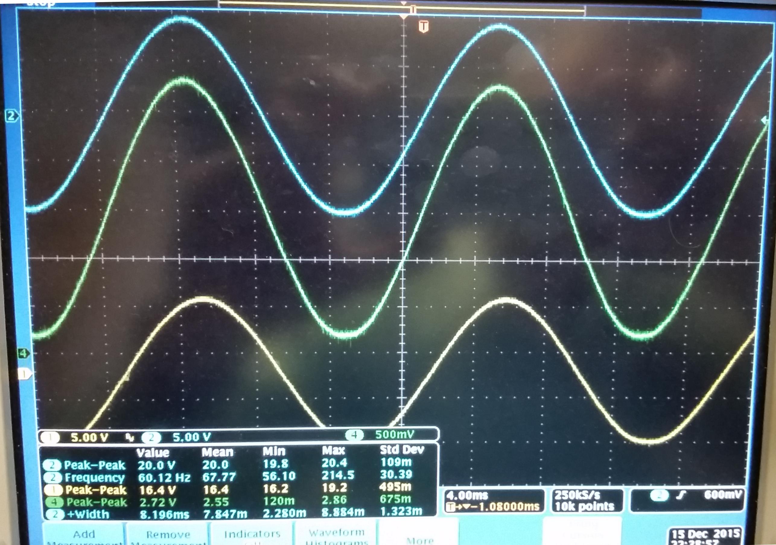
On the pictures below:

The blue trace is bipolar input from signal generator (it gets scaled down and offsetted in conditioning circuit). The green trace is input signal after conditioning: centered at 1.6V. The  yellow trace is what C28 acquires and outputs to the external DAC for diagnostic. The diagnostic signal gets converted back to bipolar signal.

My sample rate is 5 KHz, that's why yellow DAC output trace is delayed.

Any recommendations how to set ADC "more" correctly so it converts all signals?

Small slope:150 Hz frequency, 1.1V  p-p input ADC signal (green) - no distortion

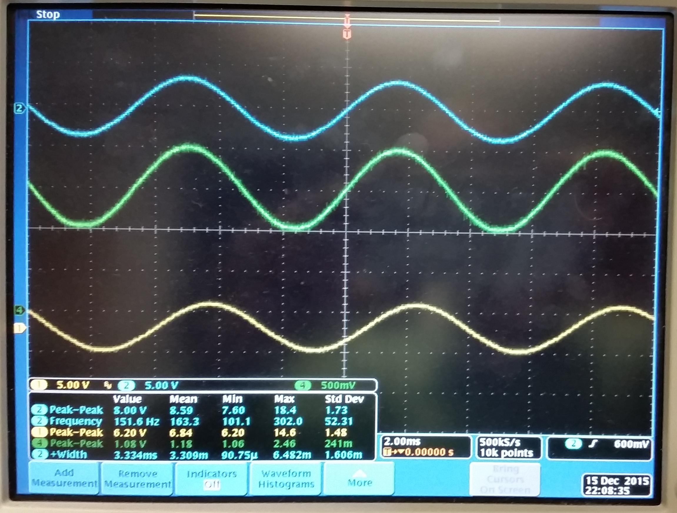
medium slope: 150 Hz frequency, 2.04V  p-p input ADC signal (green)

large slope, 150 Hz frequency, 2.2V  p-p input ADC signal (green)

Here is the proof that it is a slope, not the amplitude of the signal: 60 Hz, 2.7V p-p on ADC input is OK

  • Hi Igor,

    The ADC on this device should work fine with input frequencies into the high 100's of KHz, so lets look at a few things:

    Are you sure the problem is with the ADC samples? Could the problem be with the external DAC, or the SW that is controlling it? - Have you tried sampling a similar signal with the external 16-bit ADC, truncating the results to 12-bits, and then passing it through the same software that you are using to generate the debug waveform on the DAC? Alternately, you could load a simulated fast sine waveform into memory, and then generate that waveform with the DAC. Finally you could capture the Concerto ADC results directly in a buffer, then plot them to confirm that the issue is actually in the ADC sampled data.

    What does the impedance of the signal conditioning circuitry look like to the ADC input? Does it have a LP filter with a high series R? We provide a model of the ADC input in the device DS. You can use spice to simulate the charging of the internal S+H capacitor through your signal conditioning circuitry and the ADC input switch. If the S+H window is long enough, then the S+H capacitor should charge to within 1/2LSB or better during the allocated S+H time. If the window is too short, you can change the ACQPS setting to allow more time. Alternately, you could just increase the ACQPS setting to maximum to see if this helps (and if so, you will want to go back and do the simulations to make sure this makes sense).
  • Hi, Devin,

    What bothers me is the fact that ADC result is depending of the slope of input. I know it looks weird, and trying to get to the root. I did play with 

    RE: "Could the problem be with the external DAC, or the SW that is controlling it? - Have you tried sampling a similar signal with the external 16-bit ADC, truncating the results to 12-bits, and then passing it through the same software that you are using to generate the debug waveform on the DAC?"

    We are selling our product for couple of years, and development started 4 years ago. The firmware is pretty refined. The external DAC and ADC work fine, or we would already have some complains. Yes, I have tried putting same signal to external ADC and read it back from the same DAC. We normally dealt with slower changing signals on internal ADC input, but recently we need to acquire faster changing signal and discovered this problem.

    I put sine simultaneously to both internal and external ADC, and internal has distortions. So, I am pretty confident that it is internal ADC setup.

    RE: "What does the impedance of the signal conditioning circuitry look like to the ADC input?"

    We use the standard Concerto card from TI. thus, it has standard TI circuitry. I am aware that some channels on TI card have no anti aliasing filters, but this is observed on any channel. 

    I forgot to mention that C28 runs at 150 MHz and M3 at 75 MHz.

    It seems as if there is(are) "sticking" bit(s).  Could it be bus problem? 

    I use suggested sequence:

    a) set up reading ADC result on interrupt:

    PieVectTable.ADCINT1 = &IntADC1ISR; // start ADC1 conversion
    PieVectTable.ADCINT2 = &IntADC2ISR; // start ADC2 conversion
    PieVectTable.ADCINT3 = &IntADC3ISR; // read ADC1 conversion result
    PieVectTable.ADCINT4 = &IntADC4ISR; // read ADC2 conversion result

    b) Init ADCs

    #define ADC_usDELAY 1000L

    //---------------------------------------------------------------------------
    // InitAdc1:
    //---------------------------------------------------------------------------
    // This function initializes ADC1 to a known state.
    void InitAdc1(void)
    {
    extern void DSP28x_usDelay(Uint32 Count);

    // To powerup the ADC1 the ADC1ENCLK bit should be set first to enable
    // clocks, followed by powering up the bandgap, reference circuitry, and
    // ADC1 core.
    // Before the first conversion is performed a 5ms delay must be observed
    // after power up to give all analog circuits time to power up and settle

    // Please note that for the delay function below to operate correctly the
    // CPU_RATE define statement in the F28M35x_Examples.h file must
    // contain the correct CPU clock period in nanoseconds.
    EALLOW;
    Adc1Regs.ADCCTL1.bit.ADCBGPWD = 1; // Power ADC1 BG
    Adc1Regs.ADCCTL1.bit.ADCREFPWD = 1; // Power reference
    Adc1Regs.ADCCTL1.bit.ADCPWDN = 1; // Power ADC1
    Adc1Regs.ADCCTL1.bit.ADCENABLE = 1; // Enable ADC1
    Adc1Regs.ADCCTL1.bit.ADCREFSEL = 0; // Select interal BG
    EDIS;

    DELAY_US(ADC_usDELAY); // Delay before converting ADC1 channels
    }

    c) Then init ADC configuration

    // ADC Trigger Config
    AnalogSysctrlRegs.TRIG1SEL.all = 0x00; // Assigning ADC Trigger 1 to Nothing

    // ADC 1 Device
    Adc1Regs.ADCCTL2.bit.ADCNONOVERLAP = 1; // 0: Overlap of sample and conversion is allowed.
    // 1: Enable non-overlap mode i.e. conversion and future sampling events don't overlap
    Adc1Regs.ADCCTL2.bit.CLKDIV2EN = 0; // 0: ADC clock = ACIB clock; 1:ADC clock = ACIB clock/2
    /* Advisory ADC: ADC Result Conversion When Sampling Ends on 14th Cycle of Previous Conversion, ACQPS = 6 or 7
    Revision(s) Affected 0, A, B
    Details
    Each on-chip ADC takes 13 ADC clock cycles to complete a conversion after the
    sampling phase has ended. The result is then presented to the bus controller on the 14th
    cycle post-sampling and latched on the 15th cycle into the ADC result registers. If the
    next conversion's sampling phase terminates on this 14th cycle, the results latched by
    the bus controller into the result register are not assured to be valid across all operating
    conditions.
    Workaround(s) Some workarounds are as follows:
    • Due to the nature of the sampling and conversion phases of the ADC, there are only
    two values of ACQPS (which controls the sampling window) that would result in the
    above condition occurring—ACQPS = 6 or 7. One solution is to avoid using these
    values in ACQPS.
    • When the ADCNONOVERLAP feature (bit 1 in ADCTRL2 register) is used, the above
    condition will never be met; so the user is free to use any value of ACQPS desired.
    • Depending on the frequency of ADC sampling used in the system, the user can
    determine if their system will hit the above condition if the system requires the use of
    ACQPS = 6 or 7. For instance, if the converter is continuously converting with
    ACQPS = 6, the above condition will never be met because the end of the sampling
    phase will always fall on the 13th cycle of the current conversion in progress.
    */
    // Interrupt Configuration
    Adc1Regs.ADCCTL1.bit.INTPULSEPOS = 1; // INTerrupt Pulse Generation control - INT pulse generation occurs 1 cycle prior to ADC result latching into its result register

    Adc1Regs.INTSEL1N2.bit.INT1E = 0x01; // Enabled ADCINT1
    Adc1Regs.INTSEL1N2.bit.INT1CONT = 0x00; // Disable ADCINT1 Continuous mode
    Adc1Regs.INTSEL1N2.bit.INT1SEL = 0x00; // setup ADC1 EOC0 to trigger ADCINT1 to fire

    Adc1Regs.INTSEL3N4.bit.INT3E = 0x01; // Enabled ADCINT1
    Adc1Regs.INTSEL3N4.bit.INT3CONT = 0x00; // Disable ADCINT1 Continuous mode
    Adc1Regs.INTSEL3N4.bit.INT3SEL = 0x07; // setup ADC1 EOC7 to trigger ADCINT3 to fire

    Adc1Regs.ADCSOC0CTL.bit.TRIGSEL = 0x05; // Set SOC0 start trigger to ADC Trigger 1 of the adc
    Adc1Regs.ADCINTSOCSEL1.bit.SOC1 = 0x01; // ADCINT1 will initiate start of frame
    Adc1Regs.ADCINTSOCSEL1.bit.SOC2 = 0x01; // ADCINT1 will initiate start of frame
    Adc1Regs.ADCINTSOCSEL1.bit.SOC3 = 0x01; // ADCINT1 will initiate start of frame
    Adc1Regs.ADCINTSOCSEL1.bit.SOC4 = 0x01; // ADCINT1 will initiate start of frame
    Adc1Regs.ADCINTSOCSEL1.bit.SOC5 = 0x01; // ADCINT1 will initiate start of frame
    Adc1Regs.ADCINTSOCSEL1.bit.SOC6 = 0x01; // ADCINT1 will initiate start of frame
    Adc1Regs.ADCINTSOCSEL1.bit.SOC7 = 0x01; // ADCINT1 will initiate start of frame


    // SOC Channel configuration
    Adc1Regs.ADCSOC0CTL.bit.CHSEL = 0x00; // set SOC0 channel select to ADC1A0:ADCIN-A0
    Adc1Regs.ADCSOC1CTL.bit.CHSEL = 0x08; // set SOC6 channel select to ADC1B0:ADCIN-A1
    Adc1Regs.ADCSOC2CTL.bit.CHSEL = 0x02; // set SOC1 channel select to ADC1A2:ADCIN-A2
    Adc1Regs.ADCSOC3CTL.bit.CHSEL = 0x03; // set SOC2 channel select to ADC1A3:ADCIN-A3
    Adc1Regs.ADCSOC4CTL.bit.CHSEL = 0x04; // set SOC3 channel select to ADC1A4:ADCIN-A4
    Adc1Regs.ADCSOC5CTL.bit.CHSEL = 0x0C; // set SOC7 channel select to ADC1B4:ADCIN-A5
    Adc1Regs.ADCSOC6CTL.bit.CHSEL = 0x06; // set SOC4 channel select to ADC1A6:ADCIN-A6
    Adc1Regs.ADCSOC7CTL.bit.CHSEL = 0x07; // set SOC5 channel select to ADC1A7:ADCIN-A7
    // ADC1A2
    // SOC Acq PS config
    Adc1Regs.ADCSOC0CTL.bit.ACQPS = C28_ADC_ACQPS; // set SOC0 S/H Window
    Adc1Regs.ADCSOC1CTL.bit.ACQPS = C28_ADC_ACQPS; // set SOC1 S/H Window
    Adc1Regs.ADCSOC2CTL.bit.ACQPS = C28_ADC_ACQPS; // set SOC2 S/H Window
    Adc1Regs.ADCSOC3CTL.bit.ACQPS = C28_ADC_ACQPS; // set SOC3 S/H Window
    Adc1Regs.ADCSOC4CTL.bit.ACQPS = C28_ADC_ACQPS; // set SOC4 S/H Window
    Adc1Regs.ADCSOC5CTL.bit.ACQPS = C28_ADC_ACQPS; // set SOC5 S/H Window
    Adc1Regs.ADCSOC6CTL.bit.ACQPS = C28_ADC_ACQPS; // set SOC6 S/H Window
    Adc1Regs.ADCSOC7CTL.bit.ACQPS = C28_ADC_ACQPS; // set SOC7 S/H Window

    // Set the priority to All High in order to preserve sequence
    Adc1Regs.SOCPRICTL.bit.SOCPRIORITY = 0x10; // all SOCs are in high priority, arbitrated by SOC number (lowest)

    d) then interrupts do this:

    // First ADC Interrupt that will spawn off SOC1-7 on ADC1
    interrupt void IntADC1ISR(void) //CALLED in ElectoDamp
    {
       Adc1IntFlag = TRUE;
       // To receive more interrupts from this PIE group, acknowledge this interrupt
       Adc1Regs.ADCINTFLGCLR.bit.ADCINT1 = 1; //Clear ADCINT1 flag reinitialize
       PieCtrlRegs.PIEACK.bit.ACK1 = 1;
    }

    read register, subtract offset, convert to  Int16

    // Reads the ADC 1 SOC 0-7 Results
    interrupt void IntADC3ISR(void)
    {
    // ADC Mirror is used because the data coming out of here is right-justified and faster.
    volatile Int16 *ADCBuffPtr;

    ADCBuffPtr = (volatile Int16 *)&ADC_ISR_buff[16];

    #define IntADC_offset  1830
    *ADCBuffPtr = ((Adc1Result.ADCRESULT0 - IntADC_offset)<< 4); //index 16
    ADCBuffPtr++;
    *ADCBuffPtr = ((Adc1Result.ADCRESULT1 - IntADC_offset)<< 4); //index 17
    ADCBuffPtr++;
    *ADCBuffPtr = ((Adc1Result.ADCRESULT2 - IntADC_offset)<< 4); //index 18
    ADCBuffPtr++;
    *ADCBuffPtr = ((Adc1Result.ADCRESULT3 - IntADC_offset)<< 4); //index 19
    ADCBuffPtr++;
    *ADCBuffPtr = ((Adc1Result.ADCRESULT4 - IntADC_offset)<< 4); //index 20 Pressure Iso2 gives spikes
    ADCBuffPtr++;
    *ADCBuffPtr = ((Adc1Result.ADCRESULT5 - IntADC_offset)<< 4); //index 21
    ADCBuffPtr++;
    *ADCBuffPtr = ((Adc1Result.ADCRESULT6 - IntADC_offset)<< 4); //index 22
    ADCBuffPtr++;
    *ADCBuffPtr = ((Adc1Result.ADCRESULT7 - IntADC_offset)<< 4); //index 23

    Adc3IntFlag = TRUE; // result is ready

    // To receive more interrupts from this PIE group, acknowledge this interrupt
    Adc1Regs.ADCINTFLGCLR.bit.ADCINT3 = 1; //Clear ADCINT3 flag reinitialize
    PieCtrlRegs.PIEACK.bit.ACK10 = 1;
    }

  • Igor,

    Can you confirm that the initialization code is handling the two ACIB advisories:

    1. Analog Subsystem: Analog Subsystem Function InitAnalogSystemClock() is Incomplete
    2. Analog Subsystem: Potential Race Condition after Executing Analog Subsystem Functions AnalogClockEnable() or AnalogClockDisable()

    I don't see any symptoms that would point to these exactly, but it would eliminate known issues that might complicate the debug process.

    Can you elaborate on the "sticking bits" that you observe?  Which bus are you referring to?

    -Tommy

  • Hi, Tommy,

    I am in process of debugging it.

    I use exactly same ADC code in two different applications.

    In application "A" the ADC works fine, no issues.

    In application "B" I observe this behavior.

    In order to see timing I use three GPIO pins under C28 control, I added pin set / pin reset at the beginning and end of each interrupt

    The difference between "A" and "B":

    in "A" I initialize conversion from  timer interrupt, happens each 100 ms. Timer interrupt deals with external ADCs/DACs and processing data. The timer interrupt and "retrieving data" interrupts IntADC3ISR(), IntADC4ISR() have same priority, so retrieving happens after timer interrupt finishes.

    in "B" I initialize conversion from  the main loop. The timer interrupt happens faster, each 5 ms, and only deals with external ADCs / DACs, processing happen in the main loop. The timer interrupt and "retrieving data" interrupts IntADC3ISR(), IntADC4ISR() have same priority, so retrieving happens almost as soon as it ready. I see on scpoe monitoring diagnostic pins that conversion time changes correctly when I change ADCSOCxCTL.bit.ACQPS, but it does not affect strange behaviour.

    I compared ADC registers settings (under Registers->ADC1 in register view) in both cases and they do not have obvious difference.

    Maybe you point out what other registers I should compare?

    Question 1: is my access (READ) to register ADCxRESULT is blocked by hardware while ADC writes to it? If yes, is my access waiting or reading "something" which might not be correct? 

    Question 2: is it possible to put ADC in automatic continuous mode so it converts chosen configuration and continuously updates its ADCxRESULT registers? It would happen faster than I need, but I can read them at my pace, unless I might read "at the wrong time" while ADC writes to it. 

    I use recommended workaround (except, of cause, forever loop ESTOP0):

    void InitSysCtrl(void)

    {

         // *IMPORTANT*

        // The Device_cal function MUST be called

        // for the ADC and oscillators to function according

        // to specification. The clocks to the ADC MUST be enabled before calling

        // this function. See the device data manual and/or the ADC Reference

        // Manual for more information.


        *(unsigned int*)0x4E58 = 7; // Workaround for InitAnalogSystemClock() Advisory

      (**InitAnalogSystemClock)(C28_ADCCLK_DIVISOR); // default value = ACLKDIV4 = 3

    //  if( (**InitAnalogSystemClock)(ACLKDIV4) != 0xA005 ) {

    // If return value is not 0xA005, then analog subsystem did not initialize correctly

    //       asm ("      ESTOP0");

    //        for(;;) ;

    //    }

         EALLOW;

        // Initialize the Analog Sub-System and set the clock divider to divide by 4

        while((**AnalogClockEnable)(AnalogConfig1,ADC1_ENABLE));    // Enable ADC 1

        while((**AnalogClockEnable)(AnalogConfig2,ADC2_ENABLE));    // Enable ADC 2


        //FIX: Advisory Analog Subsystem: Potential Race Condition after Executing Analog Subsystem Functions AnalogClockEnable() or AnalogClockDisable()

        (**ReadAnalogClockStatus)(AnalogConfig2);                   // Wait for AnalogClockEnable function to finish

         // Reset both ADC in case the last reset was a debugger reset (which doesn't

        // reset the ADCs

        Adc1Regs.ADCCTL1.bit.RESET = 1;

        Adc2Regs.ADCCTL1.bit.RESET = 1;

        // Wait to ensure ADCs are out of reset before Device_Cal)() is called

        __asm(" nop");

        __asm(" nop");

         // Calibrate the device for temperature

        (**Device_Cal)();

         while((**AnalogClockDisable)(AnalogConfig1,ADC1_ENABLE));   // Disable ADC1

        while((**AnalogClockDisable)(AnalogConfig2,ADC2_ENABLE));   // Disable ADC2

        (**ReadAnalogClockStatus)(AnalogConfig2);                   // Wait for AnalogClockDisable function to finish

        EDIS;

         // Initialize the peripheral clocks

        InitPeripheralClocks();

    }

     Igor

  • Question 1: is my access (READ) to register ADCxRESULT is blocked by hardware while ADC writes to it? If yes, is my access waiting or reading "something" which might not be correct? 

    You won't ever read incorrect data, only old data, and the reading won't be corrupted by doing a CPU read at the same time the ADC HW is performing a write. 

    Question 2: is it possible to put ADC in automatic continuous mode so it converts chosen configuration and continuously updates its ADCxRESULT registers? It would happen faster than I need, but I can read them at my pace, unless I might read "at the wrong time" while ADC writes to it. 

    You can do this by setting all SOCs to trigger off of the ADCINT flag triggered by the last SOC in the chain (no need to actually allow the interrupt to propagate through the PIE to the CPU).  However, if you read these asynchronously, your samples will not be equally spaced in time.

  • Igor,

    My impression was that you had the exact same code base sampling two signals, where:

    1. Signal 1 has a slower rise/fall time and is correctly represented by the ADC results, and
    2. Signal 2 has a faster rise/fall and is not correctly represented by the ADC results

    Is my new understanding correct that you have two different software configurations for the two signal scenarios?  Have you tried using Signal 1 with Application B and Signal 2 with Application A?

    Can you toggle a GPIO pin when you software trigger the ADC conversions in application B?  I wonder if the triggers are synchronized as expected.

    All ADC reads/writes and events/triggers are serially processed over the ACIB so you would encounter bus stalls if there are simultaneous ADC requests/events.  The TRM has timing diagrams for various bus activities.

    -Tommy

  • Hi, Tommy,

    Finally, I solved the mystery.

    It is not hardware, it is our firmware. We have some functions written in assembler for speed, and I finally found that one of averaging ADC post-processing functions uses "spike detection and ignoring" with the hardcoded threshold was set too low, 256 counts per loop. After increasing this to 1024 sine went through fine. I made it as passing parameter, so I can command what threshold level to use, and this has solved the issue

    Thanks for your help!

    Igor

  • Igor,

    Thanks for reporting back with your findings. I'm glad that you were able to resolve the problem.

    -Tommy