This thread has been locked.

If you have a related question, please click the "Ask a related question" button in the top right corner. The newly created question will be automatically linked to this question.

Beginner problems with the F28377S Launchpad - Where to change the clock frequency?

Other Parts Discussed in Thread: CONTROLSUITE

Hey all,

it's me again :D

I am currently playing with the F28377S launchpad, and I am quite amazed so far. However, I am struggling with adapting my ideas into the code. In particular, I use controlsuite and its example "epwm_deadband". And I can adjust the duty cycles of my PWM channels according to what I want. However, I cannot manage to change the PWM frequency according to my calculations. The Technical Reference Manual says for Up-Down-Count mode:

T_PWM = 2*TPRD*TBCLK

I assume a processor clock frequency of 200MHz, and I would like to have a 16kHz PWM. Thus, the value for TPRD should be

TPRD = T_PWM/(2*TBCLK)=f_CLK/(2*f_PWM)=200MHz/(2*16kHz)=6250

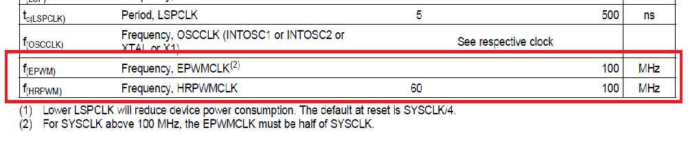
I am measuring the pins on ePWM2A and ePWM2B, which have the PRD assigned to 6250 with a duty cycle of 50% (i.e. PRD/2). On the oscilloscope, I do measure a duty cycle of 50%, exactly as wished. However, the frequency of my PWM signal is 4kHz instead of 16kHz - which is a factor of 4 smaller meaning that my microcontroller is running at 50MHz instead of 200MHz.

According to my best knowledge, the code as posted below should result in a PWM frequency of 16kHz when PRD is set to 6250, which means that the clock frequency is scaled down somewhere else.

But I cannot figure out where I have the option to scale my clock frequency. Could you maybe assist me with that?

Thank you.

The code:

//###########################################################################
// FILE:    epwm_deadband_c28.c
// TITLE:   Check PWM Dead-Band
//
//! \addtogroup cpu01_example_list
//! <h1> EPWM dead band control (epwm_deadband)</h1>
//!
//! During the test, monitor ePWM1, ePWM2, and/or ePWM3 outputs
//! on a scope.
//!
//! - ePWM1A is on GPIO0
//! - ePWM1B is on GPIO1
//! - ePWM2A is on GPIO2
//! - ePWM2B is on GPIO3
//! - ePWM3A is on GPIO4
//! - ePWM3B is on GPIO5
//!
//! This example configures ePWM1, ePWM2 and ePWM3 for:
//! - Count up/down
//! - Deadband
//!
//! 3 Examples are included:
//! - ePWM1: Active low PWMs
//! - ePWM2: Active low complementary PWMs
//! - ePWM3: Active high complementary PWMs
//!
//! Each ePWM is configured to interrupt on the 3rd zero event.
//! When this happens the deadband is modified such that
//! 0 <= DB <= DB_MAX.  That is, the deadband will move up and
//! down between 0 and the maximum value.
//!
//! View the EPWM1A/B, EPWM2A/B and EPWM3A/B waveforms
//! via an oscilloscope
//
//
//###########################################################################
// $TI Release: F2837xS Support Library v180 $
// $Release Date: Fri Nov  6 16:27:58 CST 2015 $
// $Copyright: Copyright (C) 2014-2015 Texas Instruments Incorporated -
//             http://www.ti.com/ ALL RIGHTS RESERVED $
//###########################################################################

#include "F28x_Project.h"     // Device Headerfile and Examples Include File
#include <math.h>

// Prototype statements for functions found within this file.
void InitEPwm2Example(void);
void InitEPwm6Example(void);
__interrupt void epwm2_isr(void); volatile int i; int amplitude; int steps; int offset; double Pi; void main(void) { i=0; amplitude = 1425; steps = 16000/50; offset = 1875; Pi = 3.1416; // Step 1. Initialize System Control: // PLL, WatchDog, enable Peripheral Clocks // This example function is found in the F2837xS_SysCtrl.c file. InitSysCtrl(); // Step 2. Initialize GPIO: // This example function is found in the F2837xS_Gpio.c file and // illustrates how to set the GPIO to its default state. // InitGpio(); //allocate PWM1, PWM2 and PWM3 to CPU1 // CpuSysRegs.CPUSEL0.bit.EPWM1 = 0; // CpuSysRegs.CPUSEL0.bit.EPWM2 = 0; // CpuSysRegs.CPUSEL0.bit.EPWM3 = 0; // enable PWM1, PWM2 and PWM3 CpuSysRegs.PCLKCR2.bit.EPWM2=1; // For this case just init GPIO pins for ePWM1, ePWM2, ePWM3 // These functions are in the F2837xS_EPwm.c file InitEPwm2Gpio(); InitEPwm6Gpio(); // Step 3. Clear all interrupts and initialize PIE vector table: // Disable CPU interrupts DINT; // Initialize the PIE control registers to their default state. // The default state is all PIE interrupts disabled and flags // are cleared. // This function is found in the F2837xS_PieCtrl.c file. InitPieCtrl(); // Disable CPU interrupts and clear all CPU interrupt flags: IER = 0x0000; IFR = 0x0000; // Initialize the PIE vector table with pointers to the shell Interrupt // Service Routines (ISR). // This will populate the entire table, even if the interrupt // is not used in this example. This is useful for debug purposes. // The shell ISR routines are found in F2837xS_DefaultIsr.c. // This function is found in F2837xS_PieVect.c. InitPieVectTable(); // Interrupts that are used in this example are re-mapped to // ISR functions found within this file. EALLOW; // This is needed to write to EALLOW protected registers PieVectTable.EPWM2_INT = &epwm2_isr; EDIS; // This is needed to disable write to EALLOW protected registers // Step 4. Initialize the Device Peripherals: // For this example, only initialize the ePWM EALLOW; CpuSysRegs.PCLKCR0.bit.TBCLKSYNC =0; EDIS; InitEPwm2Example(); InitEPwm6Example(); EALLOW; CpuSysRegs.PCLKCR0.bit.TBCLKSYNC =1; EDIS; // Enable CPU INT3 which is connected to EPWM1-3 INT: IER |= M_INT3; // Enable EPWM INTn in the PIE: Group 3 interrupt 1-3 PieCtrlRegs.PIEIER3.bit.INTx1 = 1; PieCtrlRegs.PIEIER3.bit.INTx2 = 1; PieCtrlRegs.PIEIER3.bit.INTx3 = 1; // Enable global Interrupts and higher priority real-time debug events: EINT; // Enable Global interrupt INTM ERTM; // Enable Global realtime interrupt DBGM // Step 6. IDLE loop. Just sit and loop forever (optional): for(;;) { asm (" NOP"); } } __interrupt void epwm2_isr(void) { i++; if(i==399) { i=0; } EPwm2Regs.CMPA.bit.CMPA = 6250/2; EPwm6Regs.CMPA.bit.CMPA=amplitude*sin(i*2*Pi/steps)+offset; // Clear INT flag for this timer EPwm2Regs.ETCLR.bit.INT = 1; // Acknowledge this interrupt to receive more interrupts from group 3 PieCtrlRegs.PIEACK.all = PIEACK_GROUP3; } void InitEPwm2Example() { EPwm2Regs.TBPRD = 6250; // Set timer period EPwm2Regs.TBPHS.bit.TBPHS = 0x0000; // Phase is 0 EPwm2Regs.TBCTR = 0x0000; // Clear counter // Setup TBCLK EPwm2Regs.TBCTL.bit.CTRMODE = TB_COUNT_UPDOWN; // Count up and down EPwm2Regs.TBCTL.bit.PHSEN = TB_DISABLE; // Disable phase loading EPwm2Regs.TBCTL.bit.HSPCLKDIV = TB_DIV1; // Clock ratio to SYSCLKOUT EPwm2Regs.TBCTL.bit.CLKDIV = TB_DIV1; // Slow just to observe on the // scope // Setup compare EPwm2Regs.CMPA.bit.CMPA = 6250/2; // Set actions EPwm2Regs.AQCTLA.bit.CAU = AQ_SET; // Set PWM2A on Zero EPwm2Regs.AQCTLA.bit.CAD = AQ_CLEAR; EPwm2Regs.AQCTLB.bit.CAU = AQ_CLEAR; // Set PWM2A on Zero EPwm2Regs.AQCTLB.bit.CAD = AQ_SET; // Active Low complementary PWMs - setup the deadband EPwm2Regs.DBCTL.bit.OUT_MODE = DB_FULL_ENABLE; EPwm2Regs.DBCTL.bit.POLSEL = DB_ACTV_LOC; EPwm2Regs.DBCTL.bit.IN_MODE = DBA_ALL; EPwm2Regs.DBRED.bit.DBRED = 0; EPwm2Regs.DBFED.bit.DBFED = 0; // Interrupt where we will modify the deadband EPwm2Regs.ETSEL.bit.INTSEL = ET_CTR_PRDZERO; // Select INT on Zero event EPwm2Regs.ETSEL.bit.INTEN = 1; // Enable INT EPwm2Regs.ETPS.bit.INTPRD = ET_1ST; // Generate INT on 1st event } void InitEPwm6Example() { EPwm6Regs.TBPRD = 6250; // Set timer period EPwm6Regs.TBPHS.bit.TBPHS = 0x0000; // Phase is 0 EPwm6Regs.TBCTR = 0x0000; // Clear counter // Setup TBCLK EPwm6Regs.TBCTL.bit.CTRMODE = TB_COUNT_UPDOWN; // Count up EPwm6Regs.TBCTL.bit.PHSEN = TB_DISABLE; // Disable phase loading EPwm6Regs.TBCTL.bit.HSPCLKDIV = TB_DIV1; // Clock ratio to SYSCLKOUT EPwm6Regs.TBCTL.bit.CLKDIV = TB_DIV1; // Slow so we can observe on // the scope // Setup compare // EPwm6Regs.CMPA.bit.CMPA = 3000; // Set actions EPwm6Regs.AQCTLA.bit.CAU = AQ_SET; // Set PWM3A on Zero EPwm6Regs.AQCTLA.bit.CAD = AQ_CLEAR; EPwm6Regs.AQCTLB.bit.CAU = AQ_CLEAR; // Set PWM3A on Zero EPwm6Regs.AQCTLB.bit.CAD = AQ_SET; // Active high complementary PWMs - Setup the deadband EPwm6Regs.DBCTL.bit.OUT_MODE = DB_FULL_ENABLE; EPwm6Regs.DBCTL.bit.POLSEL = DB_ACTV_HIC; EPwm6Regs.DBCTL.bit.IN_MODE = DBA_ALL; EPwm6Regs.DBRED.bit.DBRED = 50; EPwm6Regs.DBFED.bit.DBFED = 50; // EPwm6_DB_Direction = DB_UP; }

  • Hi Zander,

    Check this file: F2837xS_SysCtrl.c

    Regards,
    Gautam
  • Hey,

    thank you very much for your quick answer. I did go through the file F2837xS_SysCtrl.c but it is more confusing than explaining to me :)

    In that particular file, the function InitSysCtrl(void) is as posted below where the PLL is defined. I did the debugging by setting a breakpoint. And as it seems, this is what I get:

    "

     InitSysPll(XTAL_OSC,IMULT_20,FMULT_0,PLLCLK_BY_2); 		//PLLSYSCLK = (XTAL_OSC) * (IMULT + FMULT) / (PLLSYSCLKDIV)

    "

    If I do the calculation according to

    XTAL_OSC*(IMULT+FMULT)/PLLsysCLKdiv, I will get:

    1*(20+0)/1 = 20

    What does this tell me?

    void InitSysCtrl(void)
    {
        // Disable the watchdog
        DisableDog();
    
    #ifdef _FLASH
    // Copy time critical code and Flash setup code to RAM
    // This includes the following functions:  InitFlash();
    // The  RamfuncsLoadStart, RamfuncsLoadSize, and RamfuncsRunStart
    // symbols are created by the linker. Refer to the device .cmd file.
        memcpy(&RamfuncsRunStart, &RamfuncsLoadStart, (size_t)&RamfuncsLoadSize);
    
    // Call Flash Initialization to setup flash waitstates
    // This function must reside in RAM
        InitFlash_Bank0();
    #endif
    
        // *IMPORTANT*
        // The Device_cal function, which copies the ADC & oscillator calibration values
        // from TI reserved OTP into the appropriate trim registers, occurs automatically
        // in the Boot ROM. If the boot ROM code is bypassed during the debug process, the
        // following function MUST be called for the ADC and oscillators to function according
        // to specification. The clocks to the ADC MUST be enabled before calling this
        // function.
        // See the device data manual and/or the ADC Reference
        // Manual for more information.
    
        EALLOW;
    
        //enable pull-ups on unbonded IOs as soon as possible to reduce power consumption.
        GPIO_EnableUnbondedIOPullups();
    
    	CpuSysRegs.PCLKCR13.bit.ADC_A = 1;
    	CpuSysRegs.PCLKCR13.bit.ADC_B = 1;
    	CpuSysRegs.PCLKCR13.bit.ADC_C = 1;
    	CpuSysRegs.PCLKCR13.bit.ADC_D = 1;
    
        //check if device is trimmed
        if(*((Uint16 *)0x5D1B6) == 0x0000){
            //device is not trimmed, apply static calibration values
            AnalogSubsysRegs.ANAREFTRIMA.all = 31709;
            AnalogSubsysRegs.ANAREFTRIMB.all = 31709;
            AnalogSubsysRegs.ANAREFTRIMC.all = 31709;
            AnalogSubsysRegs.ANAREFTRIMD.all = 31709;
        }
    
    	CpuSysRegs.PCLKCR13.bit.ADC_A = 0;
    	CpuSysRegs.PCLKCR13.bit.ADC_B = 0;
    	CpuSysRegs.PCLKCR13.bit.ADC_C = 0;
    	CpuSysRegs.PCLKCR13.bit.ADC_D = 0;
        EDIS;
    
        // Initialize the PLL control: PLLCR and CLKINDIV
        // F28_PLLCR and F28_CLKINDIV are defined in F2837xS_Examples.h
        // Note: The internal oscillator CANNOT be used as the PLL source if the
        // PLLSYSCLK is configured to frequencies above 194 MHz.
    #ifdef _LAUNCHXL_F28377S
        InitSysPll(XTAL_OSC,IMULT_40,FMULT_0,PLLCLK_BY_2); 		//PLLSYSCLK = (XTAL_OSC) * (IMULT + FMULT) / (PLLSYSCLKDIV)
    #else
        InitSysPll(XTAL_OSC,IMULT_20,FMULT_0,PLLCLK_BY_2); 		//PLLSYSCLK = (XTAL_OSC) * (IMULT + FMULT) / (PLLSYSCLKDIV)
    #endif
    
        //Turn on all peripherals
    	InitPeripheralClocks();
    
    }
    

  • Good evening gentlemen,

    I've spent several hours trying to understand and debug the code in the F2837xS_SysCtrl.c file. I've set a breakpoint in this if-else-cause:

    #ifdef _LAUNCHXL_F28377S
        InitSysPll(XTAL_OSC,IMULT_40,FMULT_0,PLLCLK_BY_2); 		//PLLSYSCLK = (XTAL_OSC) * (IMULT + FMULT) / (PLLSYSCLKDIV)
    #else
        InitSysPll(XTAL_OSC,IMULT_20,FMULT_0,PLLCLK_BY_2); 		//PLLSYSCLK = (XTAL_OSC) * (IMULT + FMULT) / (PLLSYSCLKDIV)
    #endif

    Apparently, it is always the second option that applies. Am I right that this is the line of code that I need to change in order to change the clock frequency of my F28377S? Or am I at the wrong part of the code here?

    Looking forward to hearing from you.

    BR,

    Alexander

  • Hello again,

    I am very unhappy and disappointed about the experience with the F28377S evaluation board. While I do believe that it is a powerful microcontroller unit and very attractive for digital control applications, it is not easy to follow and modify the example codes. In particular, I do not understand why my PWM frequency does not match with my calculations according to the datasheet, which means, there is a setting somewhere that I am unable to find. I am still working on the epwm_deadband example from controlsuite, which I slightly modified. In the F2837xS_SysCtrl.c file, I define my PLL to be 200MHz (INT_OSC2*IMULT_40/PLLCLK_by_2) which gives me a PLLRAWCLK of 400MHz and thus a CPU frequency of 200MHz. According to the up-down count mode in the ePWM channel, I should expect a 16kHz PWM signal if I set PRD=6250:

    f_pwm = f_osc/(2*TBPRD) = 200MHz/(2*6250)=16kHz

    But effectively, I get a PWM of 7kHz, which is way below the target, and I do not understand why. I would appreciate if one of you would be willing to help me. By now, I actually believe that the error is not the CPU frequency anymore, but rather a scaling somewhere related to the PWM channel. The code from the epwm_deadband.c file as well as the F2837xS.c file are posted below as well as a screenshot of the oscilloscope picture:

    epwm_deadband.c:

    //###########################################################################
    // FILE:    epwm_deadband_c28.c
    // TITLE:   Check PWM Dead-Band
    //
    //! \addtogroup cpu01_example_list
    //! <h1> EPWM dead band control (epwm_deadband)</h1>
    //!
    //! During the test, monitor ePWM1, ePWM2, and/or ePWM3 outputs
    //! on a scope.
    //!
    //! - ePWM1A is on GPIO0
    //! - ePWM1B is on GPIO1
    //! - ePWM2A is on GPIO2
    //! - ePWM2B is on GPIO3
    //! - ePWM3A is on GPIO4
    //! - ePWM3B is on GPIO5
    //!
    //! This example configures ePWM1, ePWM2 and ePWM3 for:
    //! - Count up/down
    //! - Deadband
    //!
    //! 3 Examples are included:
    //! - ePWM1: Active low PWMs
    //! - ePWM2: Active low complementary PWMs
    //! - ePWM3: Active high complementary PWMs
    //!
    //! Each ePWM is configured to interrupt on the 3rd zero event.
    //! When this happens the deadband is modified such that
    //! 0 <= DB <= DB_MAX.  That is, the deadband will move up and
    //! down between 0 and the maximum value.
    //!
    //! View the EPWM1A/B, EPWM2A/B and EPWM3A/B waveforms
    //! via an oscilloscope
    //
    //
    //###########################################################################
    // $TI Release: F2837xS Support Library v180 $
    // $Release Date: Fri Nov  6 16:27:58 CST 2015 $
    // $Copyright: Copyright (C) 2014-2015 Texas Instruments Incorporated -
    //             http://www.ti.com/ ALL RIGHTS RESERVED $
    //###########################################################################
    
    #include "F28x_Project.h"     // Device Headerfile and Examples Include File
    #include <math.h>
    
    // Prototype statements for functions found within this file.
    void InitEPwm2Example(void);
    __interrupt void epwm2_isr(void);
    
    
    void main(void)
    {
    
    // Step 1. Initialize System Control:
    // PLL, WatchDog, enable Peripheral Clocks
    // This example function is found in the F2837xS_SysCtrl.c file.
        InitSysCtrl();
    
    // Step 2. Initialize GPIO:
    // This example function is found in the F2837xS_Gpio.c file and
    // illustrates how to set the GPIO to its default state.
    //    InitGpio();
    
    //allocate PWM1, PWM2 and PWM3 to CPU1
    //    CpuSysRegs.CPUSEL0.bit.EPWM1 = 0;
    //    CpuSysRegs.CPUSEL0.bit.EPWM2 = 0;
    //    CpuSysRegs.CPUSEL0.bit.EPWM3 = 0;
    
    // enable PWM1, PWM2 and PWM3
        CpuSysRegs.PCLKCR2.bit.EPWM2=1;
    
    // For this case just init GPIO pins for ePWM1, ePWM2, ePWM3
    // These functions are in the F2837xS_EPwm.c file
    	InitEPwm2Gpio();
    
    // Step 3. Clear all interrupts and initialize PIE vector table:
    // Disable CPU interrupts
        DINT;
    
    // Initialize the PIE control registers to their default state.
    // The default state is all PIE interrupts disabled and flags
    // are cleared.
    // This function is found in the F2837xS_PieCtrl.c file.
        InitPieCtrl();
    
    // Disable CPU interrupts and clear all CPU interrupt flags:
        IER = 0x0000;
        IFR = 0x0000;
    
    // Initialize the PIE vector table with pointers to the shell Interrupt
    // Service Routines (ISR).
    // This will populate the entire table, even if the interrupt
    // is not used in this example.  This is useful for debug purposes.
    // The shell ISR routines are found in F2837xS_DefaultIsr.c.
    // This function is found in F2837xS_PieVect.c.
        InitPieVectTable();
    
    // Interrupts that are used in this example are re-mapped to
    // ISR functions found within this file.
    	EALLOW; // This is needed to write to EALLOW protected registers
    	PieVectTable.EPWM2_INT = &epwm2_isr;
    	EDIS;   // This is needed to disable write to EALLOW protected registers
    
    // Step 4. Initialize the Device Peripherals:
    // For this example, only initialize the ePWM
    
    	EALLOW;
    	CpuSysRegs.PCLKCR0.bit.TBCLKSYNC =0;
    
    	EDIS;
    
    	InitEPwm2Example();
    
    	EALLOW;
    	CpuSysRegs.PCLKCR0.bit.TBCLKSYNC =1;
    
    	EDIS;
    
    
    // Enable CPU INT3 which is connected to EPWM1-3 INT:
    	IER |= M_INT3;
    
    // Enable EPWM INTn in the PIE: Group 3 interrupt 1-3
    	PieCtrlRegs.PIEIER3.bit.INTx1 = 1;
    	PieCtrlRegs.PIEIER3.bit.INTx2 = 1;
    	PieCtrlRegs.PIEIER3.bit.INTx3 = 1;
    
    
    // Enable global Interrupts and higher priority real-time debug events:
        EINT;  // Enable Global interrupt INTM
        ERTM;  // Enable Global realtime interrupt DBGM
    
    // Step 6. IDLE loop. Just sit and loop forever (optional):
        for(;;)
        {
            asm ("          NOP");
    
        }
    }
    
    __interrupt void epwm2_isr(void)
    {
        // Clear INT flag for this timer
        EPwm2Regs.ETCLR.bit.INT = 1;
    
        // Acknowledge this interrupt to receive more interrupts from group 3
        PieCtrlRegs.PIEACK.all = PIEACK_GROUP3;
    }
    
    
    void InitEPwm2Example()
    {
    
        EPwm2Regs.TBPRD = 6250;                       // Set timer period
        EPwm2Regs.TBPHS.bit.TBPHS = 0x0000;           // Phase is 0
        EPwm2Regs.TBCTR = 0x0000;                     // Clear counter
    
        // Setup TBCLK
        EPwm2Regs.TBCTL.bit.CTRMODE = TB_COUNT_UPDOWN; // Count up
        EPwm2Regs.TBCTL.bit.PHSEN = TB_DISABLE;        // Disable phase loading
        EPwm2Regs.TBCTL.bit.HSPCLKDIV = TB_DIV1;       // Clock ratio to SYSCLKOUT
        EPwm2Regs.TBCTL.bit.CLKDIV = TB_DIV1;          // Slow just to observe on the
                                                       // scope
    
        // Setup compare
        EPwm2Regs.CMPA.bit.CMPA = 6250/2;
    
        // Set actions
        EPwm2Regs.AQCTLA.bit.CAU = AQ_SET;            // Set PWM2A on Zero
        EPwm2Regs.AQCTLA.bit.CAD = AQ_CLEAR;
    
        EPwm2Regs.AQCTLB.bit.CAU = AQ_CLEAR;          // Set PWM2A on Zero
        EPwm2Regs.AQCTLB.bit.CAD = AQ_SET;
    
        // Active Low complementary PWMs - setup the deadband
        EPwm2Regs.DBCTL.bit.OUT_MODE = DB_FULL_ENABLE;
        EPwm2Regs.DBCTL.bit.POLSEL = DB_ACTV_LOC;
        EPwm2Regs.DBCTL.bit.IN_MODE = DBA_ALL;
        EPwm2Regs.DBRED.bit.DBRED = 0;
        EPwm2Regs.DBFED.bit.DBFED = 0;
    
        // Interrupt where we will modify the deadband
        EPwm2Regs.ETSEL.bit.INTSEL = ET_CTR_ZERO;     // Select INT on Zero event
        EPwm2Regs.ETSEL.bit.INTEN = 1;                // Enable INT
        EPwm2Regs.ETPS.bit.INTPRD = ET_1ST;           // Generate INT on 1st event
    
    }
    

    F2837xS_SysCtrl.c:

    //###########################################################################
    //
    // FILE:   F2837xS_SysCtrl.c
    //
    // TITLE:  F2837xS Device System Control Initialization & Support Functions.
    //
    // DESCRIPTION:
    //
    //         Example initialization of system resources.
    //
    //###########################################################################
    // $TI Release: F2837xS Support Library v180 $
    // $Release Date: Fri Nov  6 16:27:58 CST 2015 $
    // $Copyright: Copyright (C) 2014-2015 Texas Instruments Incorporated -
    //             http://www.ti.com/ ALL RIGHTS RESERVED $
    //###########################################################################
    
    #include "F2837xS_device.h"     // Headerfile Include File
    #include "F2837xS_Examples.h"   // Examples Include File
    
    // Functions that will be run from RAM need to be assigned to
    // a different section.  This section will then be mapped to a load and
    // run address using the linker cmd file.
    //
    //  *IMPORTANT*
    //  IF RUNNING FROM FLASH, PLEASE COPY OVER THE SECTION "ramfuncs"  FROM FLASH
    //  TO RAM PRIOR TO CALLING InitSysCtrl(). THIS PREVENTS THE MCU FROM THROWING
    //  AN EXCEPTION WHEN A CALL TO DELAY_US() IS MADE. 
    //
    #pragma CODE_SECTION(InitFlash_Bank0, "ramfuncs");
    #pragma CODE_SECTION(InitFlash_Bank1, "ramfuncs");
    #pragma CODE_SECTION(FlashOff_Bank0, "ramfuncs");
    #pragma CODE_SECTION(FlashOff_Bank1, "ramfuncs");
    
    void InitSysCtrl(void)
    {
        // Disable the watchdog
        DisableDog();
    
    #ifdef _FLASH
    // Copy time critical code and Flash setup code to RAM
    // This includes the following functions:  InitFlash();
    // The  RamfuncsLoadStart, RamfuncsLoadSize, and RamfuncsRunStart
    // symbols are created by the linker. Refer to the device .cmd file.
        memcpy(&RamfuncsRunStart, &RamfuncsLoadStart, (size_t)&RamfuncsLoadSize);
    
    // Call Flash Initialization to setup flash waitstates
    // This function must reside in RAM
        InitFlash_Bank0();
    #endif
    
        // *IMPORTANT*
        // The Device_cal function, which copies the ADC & oscillator calibration values
        // from TI reserved OTP into the appropriate trim registers, occurs automatically
        // in the Boot ROM. If the boot ROM code is bypassed during the debug process, the
        // following function MUST be called for the ADC and oscillators to function according
        // to specification. The clocks to the ADC MUST be enabled before calling this
        // function.
        // See the device data manual and/or the ADC Reference
        // Manual for more information.
    
        EALLOW;
    
        //enable pull-ups on unbonded IOs as soon as possible to reduce power consumption.
        GPIO_EnableUnbondedIOPullups();
    
    	CpuSysRegs.PCLKCR13.bit.ADC_A = 1;
    	CpuSysRegs.PCLKCR13.bit.ADC_B = 1;
    	CpuSysRegs.PCLKCR13.bit.ADC_C = 1;
    	CpuSysRegs.PCLKCR13.bit.ADC_D = 1;
    
        //check if device is trimmed
        if(*((Uint16 *)0x5D1B6) == 0x0000){
            //device is not trimmed, apply static calibration values
            AnalogSubsysRegs.ANAREFTRIMA.all = 31709;
            AnalogSubsysRegs.ANAREFTRIMB.all = 31709;
            AnalogSubsysRegs.ANAREFTRIMC.all = 31709;
            AnalogSubsysRegs.ANAREFTRIMD.all = 31709;
        }
    
    	CpuSysRegs.PCLKCR13.bit.ADC_A = 0;
    	CpuSysRegs.PCLKCR13.bit.ADC_B = 0;
    	CpuSysRegs.PCLKCR13.bit.ADC_C = 0;
    	CpuSysRegs.PCLKCR13.bit.ADC_D = 0;
        EDIS;
    
        // Initialize the PLL control: PLLCR and CLKINDIV
        // F28_PLLCR and F28_CLKINDIV are defined in F2837xS_Examples.h
        // Note: The internal oscillator CANNOT be used as the PLL source if the
        // PLLSYSCLK is configured to frequencies above 194 MHz.
    #ifdef _LAUNCHXL_F28377S
        InitSysPll(XTAL_OSC,IMULT_40,FMULT_0,PLLCLK_BY_2); 		//PLLSYSCLK = (XTAL_OSC) * (IMULT + FMULT) / (PLLSYSCLKDIV)
    #else
    //    InitSysPll(XTAL_OSC,IMULT_20,FMULT_0,PLLCLK_BY_2); 		//PLLSYSCLK = (XTAL_OSC) * (IMULT + FMULT) / (PLLSYSCLKDIV)
          InitSysPll(INT_OSC2,IMULT_40,FMULT_0,PLLCLK_BY_2); 		//PLLSYSCLK = (XTAL_OSC) * (IMULT + FMULT) / (PLLSYSCLKDIV)
    #endif
    
        //Turn on all peripherals
    	InitPeripheralClocks();
    
    }
    
    //---------------------------------------------------------------------------
    // InitPeripheralClocks
    //---------------------------------------------------------------------------
    // This function initializes the clocks for the peripherals. 
    //
    // Note: In order to reduce power consumption, turn off the clocks to any 
    // peripheral that is not specified for your part-number or is not used in the 
    // application
    void InitPeripheralClocks()
    {
    	EALLOW;
    
    	CpuSysRegs.PCLKCR0.bit.CLA1 = 1;
    	CpuSysRegs.PCLKCR0.bit.DMA = 1;
    	CpuSysRegs.PCLKCR0.bit.CPUTIMER0 = 1;
    	CpuSysRegs.PCLKCR0.bit.CPUTIMER1 = 1;
    	CpuSysRegs.PCLKCR0.bit.CPUTIMER2 = 1;
    	CpuSysRegs.PCLKCR0.bit.HRPWM = 1;
    	CpuSysRegs.PCLKCR0.bit.TBCLKSYNC = 1;
    
    	CpuSysRegs.PCLKCR1.bit.EMIF1 = 1;
    	CpuSysRegs.PCLKCR1.bit.EMIF2 = 1;
    
    	CpuSysRegs.PCLKCR2.bit.EPWM1 = 1;
    	CpuSysRegs.PCLKCR2.bit.EPWM2 = 1;
    	CpuSysRegs.PCLKCR2.bit.EPWM3 = 1;
    	CpuSysRegs.PCLKCR2.bit.EPWM4 = 1;
    	CpuSysRegs.PCLKCR2.bit.EPWM5 = 1;
    	CpuSysRegs.PCLKCR2.bit.EPWM6 = 1;
    	CpuSysRegs.PCLKCR2.bit.EPWM7 = 1;
    	CpuSysRegs.PCLKCR2.bit.EPWM8 = 1;
    	CpuSysRegs.PCLKCR2.bit.EPWM9 = 1;
    	CpuSysRegs.PCLKCR2.bit.EPWM10 = 1;
    	CpuSysRegs.PCLKCR2.bit.EPWM11 = 1;
    	CpuSysRegs.PCLKCR2.bit.EPWM12 = 1;
    
    	CpuSysRegs.PCLKCR3.bit.ECAP1 = 1;
    	CpuSysRegs.PCLKCR3.bit.ECAP2 = 1;
    	CpuSysRegs.PCLKCR3.bit.ECAP3 = 1;
    	CpuSysRegs.PCLKCR3.bit.ECAP4 = 1;
    	CpuSysRegs.PCLKCR3.bit.ECAP5 = 1;
    	CpuSysRegs.PCLKCR3.bit.ECAP6 = 1;
    
    	CpuSysRegs.PCLKCR4.bit.EQEP1 = 1;
    	CpuSysRegs.PCLKCR4.bit.EQEP2 = 1;
    	CpuSysRegs.PCLKCR4.bit.EQEP3 = 1;
    
    	CpuSysRegs.PCLKCR6.bit.SD1 = 1;
    	CpuSysRegs.PCLKCR6.bit.SD2 = 1;
    
    	CpuSysRegs.PCLKCR7.bit.SCI_A = 1;
    	CpuSysRegs.PCLKCR7.bit.SCI_B = 1;
    	CpuSysRegs.PCLKCR7.bit.SCI_C = 1;
    	CpuSysRegs.PCLKCR7.bit.SCI_D = 1;
    
    	CpuSysRegs.PCLKCR8.bit.SPI_A = 1;
    	CpuSysRegs.PCLKCR8.bit.SPI_B = 1;
    	CpuSysRegs.PCLKCR8.bit.SPI_C = 1;
    
    	CpuSysRegs.PCLKCR9.bit.I2C_A = 1;
    	CpuSysRegs.PCLKCR9.bit.I2C_B = 1;
    
    	CpuSysRegs.PCLKCR10.bit.CAN_A = 1;
    	CpuSysRegs.PCLKCR10.bit.CAN_B = 1;
    
    	CpuSysRegs.PCLKCR11.bit.McBSP_A = 1;
    	CpuSysRegs.PCLKCR11.bit.McBSP_B = 1;
    	CpuSysRegs.PCLKCR11.bit.USB_A = 1;
    
    	CpuSysRegs.PCLKCR12.bit.uPP_A = 1;
    
    	CpuSysRegs.PCLKCR13.bit.ADC_A = 1;
    	CpuSysRegs.PCLKCR13.bit.ADC_B = 1;
    	CpuSysRegs.PCLKCR13.bit.ADC_C = 1;
    	CpuSysRegs.PCLKCR13.bit.ADC_D = 1;
    
    	CpuSysRegs.PCLKCR14.bit.CMPSS1 = 1;
    	CpuSysRegs.PCLKCR14.bit.CMPSS2 = 1;
    	CpuSysRegs.PCLKCR14.bit.CMPSS3 = 1;
    	CpuSysRegs.PCLKCR14.bit.CMPSS4 = 1;
    	CpuSysRegs.PCLKCR14.bit.CMPSS5 = 1;
    	CpuSysRegs.PCLKCR14.bit.CMPSS6 = 1;
    	CpuSysRegs.PCLKCR14.bit.CMPSS7 = 1;
    	CpuSysRegs.PCLKCR14.bit.CMPSS8 = 1;
    
    	CpuSysRegs.PCLKCR16.bit.DAC_A = 1;
    	CpuSysRegs.PCLKCR16.bit.DAC_B = 1;
    	CpuSysRegs.PCLKCR16.bit.DAC_C = 1;
    	
    	EDIS;
    }
    
    void DisablePeripheralClocks()
    {
    	EALLOW;
    
    	CpuSysRegs.PCLKCR0.all = 0;
    	CpuSysRegs.PCLKCR1.all = 0;
    	CpuSysRegs.PCLKCR2.all = 0;
    	CpuSysRegs.PCLKCR3.all = 0;
    	CpuSysRegs.PCLKCR4.all = 0;
    	CpuSysRegs.PCLKCR6.all = 0;
    	CpuSysRegs.PCLKCR7.all = 0;
    	CpuSysRegs.PCLKCR8.all = 0;
    	CpuSysRegs.PCLKCR9.all = 0;
    	CpuSysRegs.PCLKCR10.all = 0;
    	CpuSysRegs.PCLKCR11.all = 0;
    	CpuSysRegs.PCLKCR12.all = 0;
    	CpuSysRegs.PCLKCR13.all = 0;
    	CpuSysRegs.PCLKCR14.all = 0;
    	CpuSysRegs.PCLKCR16.all = 0;
    	
    	EDIS;
    }
    
    //---------------------------------------------------------------------------
    // Example: InitFlash_Bank0
    //---------------------------------------------------------------------------
    // This function initializes the Flash Control registers for Bank0
    
    void InitFlash_Bank0(void)
    {
        EALLOW;
    
        // set VREADST to the proper value for the
        // flash banks to power up properly
        // This sets the bank power up delay
        Flash0CtrlRegs.FBAC.bit.VREADST = 0x14;
    
        //At reset bank and pump are in sleep
        //A Flash access will power up the bank and pump automatically
        //After a Flash access, bank and pump go to low power mode (configurable in FBFALLBACK/FPAC1 registers)-
        //if there is no further access to flash
        //Power up Flash bank and pump and this also sets the fall back mode of flash and pump as active
        Flash0CtrlRegs.FPAC1.bit.PMPPWR = 0x1;
        Flash0CtrlRegs.FBFALLBACK.bit.BNKPWR0 = 0x3;
    
        //Disable Cache and prefetch mechanism before changing wait states
        Flash0CtrlRegs.FRD_INTF_CTRL.bit.DATA_CACHE_EN = 0;
        Flash0CtrlRegs.FRD_INTF_CTRL.bit.PREFETCH_EN = 0;
    
        //Set waitstates according to frequency
        //                CAUTION
        //Minimum waitstates required for the flash operating
        //at a given CPU rate must be characterized by TI.
        //Refer to the datasheet for the latest information.
        #if CPU_FRQ_200MHZ
        Flash0CtrlRegs.FRDCNTL.bit.RWAIT = 0x3;
        #endif
    
        #if CPU_FRQ_150MHZ
        Flash0CtrlRegs.FRDCNTL.bit.RWAIT = 0x2;
        #endif
    
        #if CPU_FRQ_120MHZ
        Flash0CtrlRegs.FRDCNTL.bit.RWAIT = 0x2;
        #endif
    
        //Enable Cache and prefetch mechanism to improve performance
        //of code executed from Flash.
        Flash0CtrlRegs.FRD_INTF_CTRL.bit.DATA_CACHE_EN = 1;
        Flash0CtrlRegs.FRD_INTF_CTRL.bit.PREFETCH_EN = 1;
    
        //At reset, ECC is enabled
        //If it is disabled by application software and if application again wants to enable ECC
        Flash0EccRegs.ECC_ENABLE.bit.ENABLE = 0xA;
    
        EDIS;
    
        //Force a pipeline flush to ensure that the write to
        //the last register configured occurs before returning.
    
        __asm(" RPT #7 || NOP");
    
    }
    
    //---------------------------------------------------------------------------
    // Example: InitFlash_Bank1
    //---------------------------------------------------------------------------
    // This function initializes the Flash Control registers for Bank1
    
    void InitFlash_Bank1(void)
    {
        EALLOW;
    
        // set VREADST to the proper value for the
        // flash banks to power up properly
        // This sets the bank power up delay
        Flash1CtrlRegs.FBAC.bit.VREADST = 0x14;
    
        //At reset bank and pump are in sleep
        //A Flash access will power up the bank and pump automatically
        //After a Flash access, bank and pump go to low power mode (configurable in FBFALLBACK/FPAC1 registers)-
        //if there is no further access to flash
        //Power up Flash bank and pump and this also sets the fall back mode of flash and pump as active
        Flash1CtrlRegs.FPAC1.bit.PMPPWR = 0x1;
        Flash1CtrlRegs.FBFALLBACK.bit.BNKPWR0 = 0x3;
    
        //Disable Cache and prefetch mechanism before changing wait states
        Flash1CtrlRegs.FRD_INTF_CTRL.bit.DATA_CACHE_EN = 0;
        Flash1CtrlRegs.FRD_INTF_CTRL.bit.PREFETCH_EN = 0;
    
        //Set waitstates according to frequency
        //                CAUTION
        //Minimum waitstates required for the flash operating
        //at a given CPU rate must be characterized by TI.
        //Refer to the datasheet for the latest information.
        #if CPU_FRQ_200MHZ
        Flash1CtrlRegs.FRDCNTL.bit.RWAIT = 0x3;
        #endif
    
        #if CPU_FRQ_150MHZ
        Flash1CtrlRegs.FRDCNTL.bit.RWAIT = 0x2;
        #endif
    
        #if CPU_FRQ_120MHZ
        Flash1CtrlRegs.FRDCNTL.bit.RWAIT = 0x2;
        #endif
    
        //Enable Cache and prefetch mechanism to improve performance
        //of code executed from Flash.
        Flash1CtrlRegs.FRD_INTF_CTRL.bit.DATA_CACHE_EN = 1;
        Flash1CtrlRegs.FRD_INTF_CTRL.bit.PREFETCH_EN = 1;
    
        //At reset, ECC is enabled
        //If it is disabled by application software and if application again wants to enable ECC
        Flash1EccRegs.ECC_ENABLE.bit.ENABLE = 0xA;
    
        EDIS;
    
        //Force a pipeline flush to ensure that the write to
        //the last register configured occurs before returning.
    
        __asm(" RPT #7 || NOP");
    
    }
    
    //---------------------------------------------------------------------------
    // Example: FlashOff_Bank0():
    //---------------------------------------------------------------------------
    // This function powers down the flash
    
    //                   CAUTION
    // This function MUST be executed out of RAM. Executing it
    // out of OTP/Flash will yield unpredictable results.
    // Also you must seize the flash pump for the correct flash wrapper
    // in order to power it down.
    
    void FlashOff_Bank0(void)
    {
    	EALLOW;
    
    	// set VREADST to the proper value for the
    	// flash banks to power up properly
    	Flash0CtrlRegs.FBAC.bit.VREADST = 0x14;
    
    	// power down bank
    	Flash0CtrlRegs.FBFALLBACK.bit.BNKPWR0 = 0;
    	// power down pump
    	Flash0CtrlRegs.FPAC1.bit.PMPPWR = 0;
    
    	EDIS;
    }
    
    //---------------------------------------------------------------------------
    // Example: FlashOff_Bank1():
    //---------------------------------------------------------------------------
    // This function powers down the flash
    
    //                   CAUTION
    // This function MUST be executed out of RAM. Executing it
    // out of OTP/Flash will yield unpredictable results.
    // Also you must seize the flash pump for the correct flash wrapper
    // in order to power it down.
    
    void FlashOff_Bank1(void)
    {
    	EALLOW;
    
    	// set VREADST to the proper value for the
    	// flash banks to power up properly
    	Flash1CtrlRegs.FBAC.bit.VREADST = 0x14;
    
    	// power down bank
    	Flash1CtrlRegs.FBFALLBACK.bit.BNKPWR0 = 0;
    	// power down pump
    	Flash1CtrlRegs.FPAC1.bit.PMPPWR = 0;
    
    	EDIS;
    }
    
    //---------------------------------------------------------------------------
    // Example: SeizeFlashPump_Bank0():
    //---------------------------------------------------------------------------
    // Wait until the flash pump for bank0 is available, then take control of it 
    // using the flash pump Semaphore.
    
    void SeizeFlashPump_Bank0()
    {
    	EALLOW;
    
        while (FlashPumpSemaphoreRegs.PUMPREQUEST.bit.PUMP_OWNERSHIP != 0x2)
        {
            FlashPumpSemaphoreRegs.PUMPREQUEST.all = IPC_PUMP_KEY | 0x2;
        }
    
    	EDIS;
    }
    
    //---------------------------------------------------------------------------
    // Example: SeizeFlashPump_Bank1():
    //---------------------------------------------------------------------------
    // Wait until the flash pump for bank1 is available, then take control of it 
    // using the flash pump Semaphore.
    
    void SeizeFlashPump_Bank1()
    {
    	EALLOW;
    
        while (FlashPumpSemaphoreRegs.PUMPREQUEST.bit.PUMP_OWNERSHIP != 0x1)
        {
            FlashPumpSemaphoreRegs.PUMPREQUEST.all = IPC_PUMP_KEY | 0x1;
        }
    
    	EDIS;
    }
    
    //---------------------------------------------------------------------------
    // Example: ReleaseFlashPump():
    //---------------------------------------------------------------------------
    //Release control of the flash pump using the flash pump semaphore
    
    void ReleaseFlashPump()
    {
    	EALLOW;
    	FlashPumpSemaphoreRegs.PUMPREQUEST.all = IPC_PUMP_KEY | 0x0;
    	EDIS;
    }
    
    //---------------------------------------------------------------------------
    // Example: ServiceDog:
    //---------------------------------------------------------------------------
    // This function resets the watchdog timer.
    // Enable this function for using ServiceDog in the application
    
    void ServiceDog(void)
    {
        EALLOW;
        WdRegs.WDKEY.bit.WDKEY = 0x0055;
        WdRegs.WDKEY.bit.WDKEY = 0x00AA;
        EDIS;
    }
    
    //---------------------------------------------------------------------------
    // Example: DisableDog:
    //---------------------------------------------------------------------------
    // This function disables the watchdog timer.
    
    void DisableDog(void)
    {
    	volatile Uint16 temp;
        EALLOW;
        //Grab the clock config so we don't clobber it
        temp = WdRegs.WDCR.all & 0x0007;
        WdRegs.WDCR.all = 0x0068 | temp;
        EDIS;
    }
    
    //---------------------------------------------------------------------------
    // Example: InitPll:
    //---------------------------------------------------------------------------
    // This function initializes the PLL registers.
    //
    // Note: The internal oscillator CANNOT be used as the PLL source if the
    // PLLSYSCLK is configured to frequencies above 194 MHz.
    
    void InitSysPll(Uint16 clock_source, Uint16 imult, Uint16 fmult, Uint16 divsel)
    {
        if((clock_source == ClkCfgRegs.CLKSRCCTL1.bit.OSCCLKSRCSEL)    &&
          (imult         == ClkCfgRegs.SYSPLLMULT.bit.IMULT)           &&
          (fmult         == ClkCfgRegs.SYSPLLMULT.bit.FMULT)           &&
          (divsel        == ClkCfgRegs.SYSCLKDIVSEL.bit.PLLSYSCLKDIV))
        {
            //everything is set as required, so just return
            return;
        }
    
        if(clock_source != ClkCfgRegs.CLKSRCCTL1.bit.OSCCLKSRCSEL)
        {
            switch (clock_source)
            {
                case INT_OSC1:
                    SysIntOsc1Sel();
                    break;
    
                case INT_OSC2:
                    SysIntOsc2Sel();
                    break;
    
                case XTAL_OSC:
                    SysXtalOscSel();
                    break;
            }
        }
    
        EALLOW;
         // first modify the PLL multipliers
        if(imult != ClkCfgRegs.SYSPLLMULT.bit.IMULT || fmult != ClkCfgRegs.SYSPLLMULT.bit.FMULT)
        {
            // Bypass PLL and set dividers to /1
            ClkCfgRegs.SYSPLLCTL1.bit.PLLCLKEN = 0;
            ClkCfgRegs.SYSCLKDIVSEL.bit.PLLSYSCLKDIV = 0;
    
            // Program PLL multipliers
            Uint32 temp_syspllmult = ClkCfgRegs.SYSPLLMULT.all;
            ClkCfgRegs.SYSPLLMULT.all = ((temp_syspllmult & ~(0x37FU)) | 
                                         ((fmult << 8U) | imult));
                                         
            ClkCfgRegs.SYSPLLCTL1.bit.PLLEN = 1;            // Enable SYSPLL
    
            // Wait for the SYSPLL lock
            while(ClkCfgRegs.SYSPLLSTS.bit.LOCKS != 1)
            {
                // Uncomment to service the watchdog
                // ServiceDog();
            }
    
            // Write a multiplier again to ensure proper PLL initialization
            // This will force the PLL to lock a second time
            ClkCfgRegs.SYSPLLMULT.bit.IMULT = imult;        // Setting integer multiplier
    
            // Wait for the SYSPLL re-lock
            while(ClkCfgRegs.SYSPLLSTS.bit.LOCKS != 1)
            {
                // Uncomment to service the watchdog
                // ServiceDog();
            }
        }
    
        // Set divider to produce slower output frequency to limit current increase
        if(divsel != PLLCLK_BY_126)
        {
             ClkCfgRegs.SYSCLKDIVSEL.bit.PLLSYSCLKDIV = divsel + 1;
        }else
        {
             ClkCfgRegs.SYSCLKDIVSEL.bit.PLLSYSCLKDIV = divsel;
        }
    
        // Enable PLLSYSCLK is fed from system PLL clock
        ClkCfgRegs.SYSPLLCTL1.bit.PLLCLKEN = 1;
    
        // Small 100 cycle delay
        asm(" RPT #100 || NOP");
    
        // Set the divider to user value
        ClkCfgRegs.SYSCLKDIVSEL.bit.PLLSYSCLKDIV = divsel;
        EDIS;
    }
    
    
    //---------------------------------------------------------------------------
    // Example: InitPll2:
    //---------------------------------------------------------------------------
    // This function initializes the PLL2 registers.
    //
    // Note: The internal oscillator CANNOT be used as the PLL source if the
    // PLLSYSCLK is configured to frequencies above 194 MHz.
    
    void InitAuxPll(Uint16 clock_source, Uint16 imult, Uint16 fmult, Uint16 divsel)
    {
    	Uint16 temp_divsel;
    
    	if((clock_source == ClkCfgRegs.CLKSRCCTL2.bit.AUXOSCCLKSRCSEL)   &&
    	  (imult		 == ClkCfgRegs.AUXPLLMULT.bit.IMULT) 	      &&
    	  (fmult 	     == ClkCfgRegs.AUXPLLMULT.bit.FMULT)          &&
    	  (divsel        == ClkCfgRegs.AUXCLKDIVSEL.bit.AUXPLLDIV))
        {
    	    //everything is set as required, so just return
    	    return;
    	}
    
    	switch (clock_source)
    	{
    
    		case INT_OSC2:
    			AuxIntOsc2Sel();
    			break;
    
    		case XTAL_OSC:
    			AuxXtalOscSel();
    			break;
    
    		case AUXCLKIN:
    			AuxAuxClkSel();
    			break;
    
    	}
    
       // Change the SYSPLL Integer Multiplier (or) SYSPLL Fractional Multiplier
       if(ClkCfgRegs.AUXPLLMULT.bit.IMULT != imult || ClkCfgRegs.AUXPLLMULT.bit.FMULT !=fmult)
       {
    	   EALLOW;
    	   ClkCfgRegs.AUXCLKDIVSEL.bit.AUXPLLDIV = AUXPLLRAWCLK_BY_8;
    //	   ClkCfgRegs.AUXCLKDIVSEL.bit.AUXPLLDIV = AUXPLLRAWCLK_BY_1;
           
           //Set integer and fractional multiplier     
           Uint32 temp_auxpllmult = ClkCfgRegs.AUXPLLMULT.all;
           ClkCfgRegs.AUXPLLMULT.all = ((temp_auxpllmult & ~(0x37FU)) | 
                                        ((fmult << 8U) | imult));
                                        
    	   ClkCfgRegs.AUXPLLCTL1.bit.PLLEN = 1;			//Enable AUXPLL
    	   EDIS;
    
    	   //Wait for the AUXPLL lock
    	   while(ClkCfgRegs.AUXPLLSTS.bit.LOCKS != 1)
    	   {
    	        // Uncomment to service the watchdog
    	        // ServiceDog();
    	   }
           
           // Write a multiplier again to ensure proper PLL initialization
           // This will force the PLL to lock a second time
           EALLOW;
           ClkCfgRegs.AUXPLLMULT.bit.IMULT = imult;        // Setting integer multiplier       
           EDIS;
           
           //Wait for the AUXPLL lock
    	   while(ClkCfgRegs.AUXPLLSTS.bit.LOCKS != 1)
    	   {
    	        // Uncomment to service the watchdog
    	        // ServiceDog();
    	   }
       }
    
    	 //increase the freq. of operation in steps to avoid any VDD fluctuations
    	 temp_divsel = AUXPLLRAWCLK_BY_8;
    //	 temp_divsel = AUXPLLRAWCLK_BY_1;
    	 while(ClkCfgRegs.AUXCLKDIVSEL.bit.AUXPLLDIV != divsel)
    	 {
    		 EALLOW;
    		 ClkCfgRegs.AUXCLKDIVSEL.bit.AUXPLLDIV = temp_divsel - 1;
    		 EDIS;
    
    		 temp_divsel = temp_divsel - 1;
    		 if(ClkCfgRegs.AUXCLKDIVSEL.bit.AUXPLLDIV != divsel)
    		 {
    			 DELAY_US(15L);
    		 }
    	 }
    
       EALLOW;
       ClkCfgRegs.AUXPLLCTL1.bit.PLLCLKEN = 1;			//Enable AUXPLLCLK is fed from AUX PLL
       EDIS;
    }
    
    //---------------------------------------------------------------------------
    // Example: CsmUnlock:
    //---------------------------------------------------------------------------
    // This function unlocks the CSM. User must replace 0xFFFF's with current
    // password for the DSP. Returns 1 if unlock is successful.
    
    #define STATUS_FAIL          0
    #define STATUS_SUCCESS       1
    
    Uint16 CsmUnlock()
    {
        volatile Uint16 temp;
    
        // Load the key registers with the current password. The 0xFFFF's are dummy
        // passwords.  User should replace them with the correct password for the DSP.
    
        EALLOW;
    //    CsmRegs.KEY0 = 0xFFFF;
    //    CsmRegs.KEY1 = 0xFFFF;
    //    CsmRegs.KEY2 = 0xFFFF;
    //    CsmRegs.KEY3 = 0xFFFF;
    //    CsmRegs.KEY4 = 0xFFFF;
    //    CsmRegs.KEY5 = 0xFFFF;
    //    CsmRegs.KEY6 = 0xFFFF;
    //    CsmRegs.KEY7 = 0xFFFF;
    
        DcsmZ1Regs.Z1_CSMKEY0 = 0xFFFFFFFF;
        DcsmZ1Regs.Z1_CSMKEY1 = 0xFFFFFFFF;
        DcsmZ1Regs.Z1_CSMKEY2 = 0xFFFFFFFF;
        DcsmZ1Regs.Z1_CSMKEY3  = 0xFFFFFFFF;
    
        DcsmZ2Regs.Z2_CSMKEY0 = 0xFFFFFFFF;
        DcsmZ2Regs.Z2_CSMKEY1 = 0xFFFFFFFF;
        DcsmZ2Regs.Z2_CSMKEY2 = 0xFFFFFFFF;
        DcsmZ2Regs.Z2_CSMKEY3  = 0xFFFFFFFF;
        EDIS;
    
        // Perform a dummy read of the password locations
        // if they match the key values, the CSM will unlock
    
    //    temp = CsmPwl.PSWD0;
    //    temp = CsmPwl.PSWD1;
    //    temp = CsmPwl.PSWD2;
    //    temp = CsmPwl.PSWD3;
    //    temp = CsmPwl.PSWD4;
    //    temp = CsmPwl.PSWD5;
    //    temp = CsmPwl.PSWD6;
    //    temp = CsmPwl.PSWD7;
    
        // If the CSM unlocked, return success, otherwise return
        // failure.
    //    if (CsmRegs.CSMSCR.bit.SECURE == 0) return STATUS_SUCCESS;
    //    else return STATUS_FAIL;
    
        return 0;
    
    }
    
    //---------------------------------------------------------------------------
    // Example: SysIntOsc1Sel:
    //---------------------------------------------------------------------------
    // This function switches to Internal Oscillator 1 and turns off all other clock
    // sources to minimize power consumption
    
    void SysIntOsc1Sel (void) {
        EALLOW;
        ClkCfgRegs.CLKSRCCTL1.bit.OSCCLKSRCSEL = 2; // Clk Src = INTOSC1
        EDIS;
    }
    
    //---------------------------------------------------------------------------
    // Example: SysIntOsc2Sel:
    //---------------------------------------------------------------------------
    // This function switches to Internal oscillator 2 from External Oscillator
    // and turns off all other clock sources to minimize power consumption
    // NOTE: If there is no external clock connection, when switching from
    //       INTOSC1 to INTOSC2, EXTOSC and XLCKIN must be turned OFF prior
    //       to switching to internal oscillator 1
    
    void SysIntOsc2Sel (void) {
    
        EALLOW;
        ClkCfgRegs.CLKSRCCTL1.bit.INTOSC2OFF=0;     // Turn on INTOSC2
        ClkCfgRegs.CLKSRCCTL1.bit.OSCCLKSRCSEL = 0; // Clk Src = INTOSC2
        EDIS;
    
    }
    
    //---------------------------------------------------------------------------
    // Example: SysXtalOscSel:
    //---------------------------------------------------------------------------
    // This function switches to External CRYSTAL oscillator and turns off all other clock
    // sources to minimize power consumption. This option may not be available on all
    // device packages
    
    void SysXtalOscSel (void)  {
    
        EALLOW;
        ClkCfgRegs.CLKSRCCTL1.bit.XTALOFF=0;        // Turn on XTALOSC
        ClkCfgRegs.CLKSRCCTL1.bit.OSCCLKSRCSEL = 1; // Clk Src = XTAL
        EDIS;
    
    }
    
    //---------------------------------------------------------------------------
    // Example: AuxIntOsc2Sel:
    //---------------------------------------------------------------------------
    // This function switches to Internal oscillator 2 from External Oscillator
    // and turns off all other clock sources to minimize power consumption
    // NOTE: If there is no external clock connection, when switching from
    //       INTOSC1 to INTOSC2, EXTOSC and XLCKIN must be turned OFF prior
    //       to switching to internal oscillator 1
    
    void AuxIntOsc2Sel (void) {
    
        EALLOW;
        ClkCfgRegs.CLKSRCCTL1.bit.INTOSC2OFF=0;     // Turn on INTOSC2
        ClkCfgRegs.CLKSRCCTL2.bit.AUXOSCCLKSRCSEL = 0; // Clk Src = INTOSC2
        EDIS;
    
    }
    
    //---------------------------------------------------------------------------
    // Example: AuxXtalOscSel:
    //---------------------------------------------------------------------------
    // This function switches to External CRYSTAL oscillator and turns off all other clock
    // sources to minimize power consumption. This option may not be available on all
    // device packages
    
    void AuxXtalOscSel (void)  {
    
        EALLOW;
        ClkCfgRegs.CLKSRCCTL1.bit.XTALOFF=0;        // Turn on XTALOSC
        ClkCfgRegs.CLKSRCCTL2.bit.AUXOSCCLKSRCSEL = 1; // Clk Src = XTAL
        EDIS;
    
    }
    
    //---------------------------------------------------------------------------
    // Example: AuxAUXCLKOscSel:
    //---------------------------------------------------------------------------
    // This function switches to External CRYSTAL oscillator and turns off all other clock
    // sources to minimize power consumption. This option may not be available on all
    // device packages
    
    void AuxAuxClkSel (void)  {
    
        EALLOW;
        ClkCfgRegs.CLKSRCCTL2.bit.AUXOSCCLKSRCSEL = 2; // Clk Src = XTAL
        EDIS;
    
    }
    
    
    //Enter IDLE mode
    void IDLE()
    {
    	EALLOW;
    	CpuSysRegs.LPMCR.bit.LPM = LPM_IDLE;
    	EDIS;
    	asm(" IDLE");
    }
    
    //Enter STANDBY mode
    void STANDBY()
    {
    	EALLOW;
    	CpuSysRegs.LPMCR.bit.LPM = LPM_STANDBY;
    	EDIS;
    	asm(" IDLE");
    }
    
    //Enter HALT mode
    void HALT()
    {
        EALLOW;
        CpuSysRegs.LPMCR.bit.LPM = LPM_HALT;
        ClkCfgRegs.SYSPLLCTL1.bit.PLLCLKEN = 0;
        ClkCfgRegs.SYSPLLCTL1.bit.PLLEN = 0;
        EDIS;
        asm(" IDLE");
    }
    
    //Enter HIB mode
    void HIB()
    {
        EALLOW;
        CpuSysRegs.LPMCR.bit.LPM = LPM_HIB;
        EDIS;
        DisablePeripheralClocks();
        EALLOW;
        ClkCfgRegs.SYSPLLCTL1.bit.PLLCLKEN = 0;
        ClkCfgRegs.SYSPLLCTL1.bit.PLLEN = 0;
        EDIS;
        asm(" IDLE");   
    }
    

    A picture of the measured PWM:

  • Hi Alexander,

    On this device the maximum operating frq for ePWM module is 100 MHz. So even though CPU is running at 200MHz, the ePWM frq is 100 MHz and that is why you see 1/2 the value.

    This information is captured in datasheet as well as TRM.

    In TRM see the "Figure 2-5. Clocking System" which should the clock divider for PWM. This clock divider is controlled by "EPWMCLKDIV" field of

    PERCLKDIVSEL register (detail given in Figure 2-151. PERCLKDIVSEL Register).

    In datasheet "Table 5-12. Internal Clock Frequencies" has this information captured.

     Hope this clarifies the issue.

    Regards,

    Vivek Singh

  • There is an additional EPWM clock divider, which, by default is is SYSCLK/2. ClkCfgRegs.PerCLKDIVSEL.EPWMCLKDIV. You can verify your SYSCLK by enabling XCLKOUT.

    I am not sure of the top of my head if the on board oscillator of the Launchpad is a 10MHz or 20MHz. you will want to verify that as well by checking out the Launchpad schematics.

    Refer to the Clocking section of the System Control Chapter of the F2837xS TRM for more information on the clocking schemes of this device.

    -Mark
  • Hello Vivek and Mark,

    I sincerely thank you for your quick reply and your help. It is working perfectly fine now and this particular issue is solved. In fact, two things caused the issue:

    1. the external oscillator on the Launchpad connected to the XTAL pins of the microcontroller is running at 10MHz (and not wrongly assumed to be 15MHz) whereas the example in the TRM uses 15MHz. Unfortunately, I relied on the example in the TRM rather than checking out the Launchpad schematics. 

    2. I finally figured out on how to change the EPWMCLKDIV to the proper value. 

    With these two things, I now get the PWM to be consistent with the formula from the TRM.

    You guys really saved my weekend.

    All the best,

    Alex

  • Hi Alex,

    Good to know that you got this working. Have a good weekend.

    Regards,

    Vivek Singh