This thread has been locked.

If you have a related question, please click the "Ask a related question" button in the top right corner. The newly created question will be automatically linked to this question.

Illegal_ISR on TMX320F28377D CPU2

Other Parts Discussed in Thread: TMS320F28377D

Dear TI community,

I have been facing an issue in my code and I have run out of ideas so far. I am wondering if I am missing a detail regarding the dual core structure of the TMX320F28377D. Control card R1.1.

I have two projects almost identical running on each CPU mostly it differs on the linker. CPU1 runs with no issues but on CPU2, on the first time I run the code, I get into an Illegal_ISR.

If I do a CPU Reset and Restart then the code run stable. I cannot understand or identify what changes from the first run to the second after the reset.

Here is a screenshot. The address 0x01701C is RAM assign to data so clearly the code is jumping to weird address.
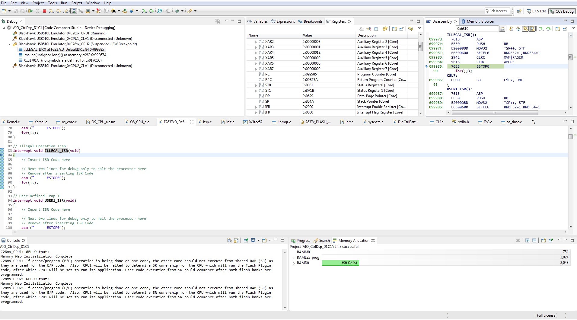
If I debug step by step I can move forward in the code. But when I hit 'Play' then I get to the Illegal_ISR. Any idea is welcomed!

Thanks,

Matias

  • Hi Matias,

    Are you using GSx RAM for code execution? If yes then please make sure it's master ownership (MSEL_GSx bit configuration in GSxMSEL register) is changed to CPU2 by CPU1 code before CPU2 start executing from that RAM.

    Regards,

    Vivek Singh

  • Hi Vivek,

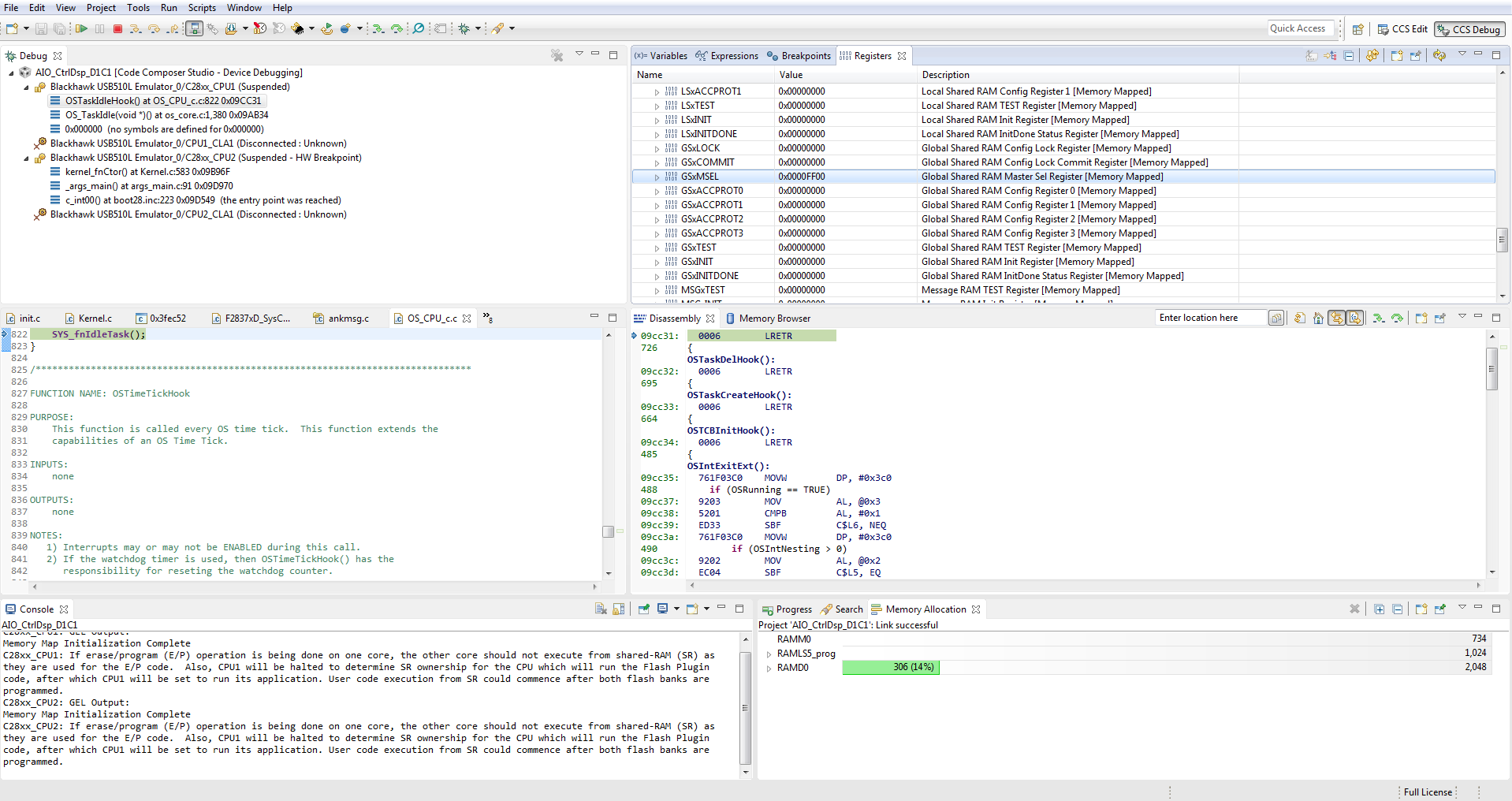
    Thanks for the reply. GSRAM0 to 7 are for CPU1 and GSRAM8 to 15 are for CPU2. For this GSxMSEL is set to 0xFF00.

    Ramfunc for initFlash() are run from RAMD0.

    Matias

  • Based on other threads, basically I have checked the memory for permission. Code for InitFlash is correctly running from RAM.

    I load both CPUs and allow CPU1 to fully start before starting CPU2. It is just that the first time, CPU2 wont start and get to this illegal_ISR().

    Should I code a handshake between CPUs?

    Thanks again,

    Matias

  • Hi Matias,

    Should I code a handshake between CPUs?

    Yes, that is always recommended to make sure CPU2 does not start before CPU1 is done with device initialization.

    Before starting CPU2, can you check the value of MSEL bit fields for GSxRAMs which CPU2 is going to use, via CPU1 memory watch window.

    Regards,

    Vivek Singh

  • Hi Vivek,

    Nice hearing from you again. I can confirm that the GSxRAM register is correctly populated.

    Matias

  • Matias,

    In this snapshot CPU2 is halted inside main which means it has already jumped into main. It'll be good to check the status of this just by running the CPU1 code (CPU2 is halted at reset vector). If you see the values correct in that case as well then you need to step through CPU2 code to see when it goes into Illegal_ISR.

    Regards,

    Vivek Singh 

  • Hi vivek,

    You are right and it is what I did. The GSxMSEL register was verified before running CPU2.

    Matias
  • Ok. Can you step through the CPU2 code to know which part of the code is causing the Illegal_ISR and from which memory location that code is running.

    Regards,

    Vivek Singh

  • Hi Vivek, thanks for taking the time to follow up. At the beginning I thought the error was not consistent but it turns out it is. 

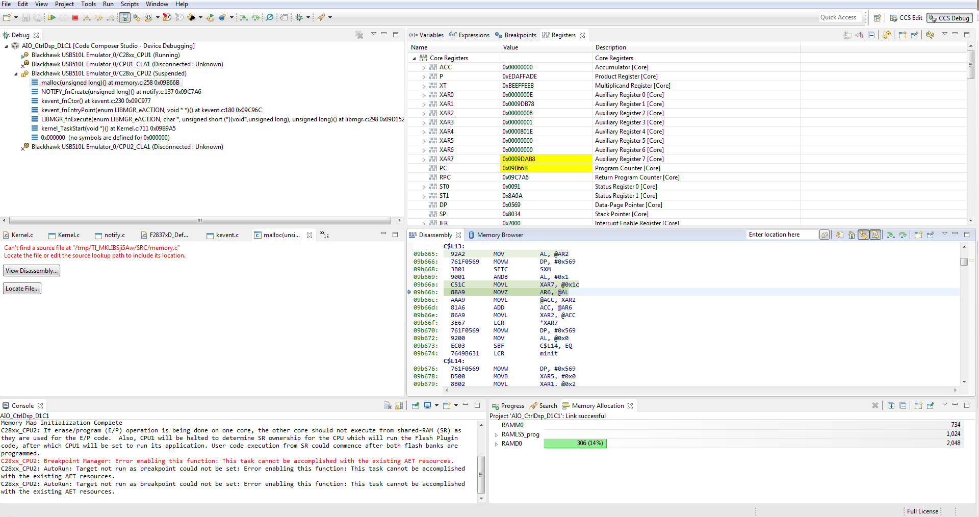
    At a point in the code a malloc() is called. Upon returning it seems that a pointer is not recovered correctly to XAR7 and the code jumps to 0x00000.

    Interestingly, the code crushes the first time, but after a reset, the execution of the code is good. I am going through the assembly code to understand the problem. If you have any hint would help.

    Thanks a lot!

  • Hello Vivek and the rest of the community,

    If I may: I am still struggling with this problem. Basically, the following instruction is suppose to load a pointer on XAR7 but it is not doing on the first attempt after loading the code

    09a8f7:   C51C        MOVL         XAR7, @0x1c

    The fact is I do not know where is this pointing to, what kind of data it is...? Cannot find it in RAM.

    Thanks again,

    Matias 

  • Hi Matias,

    The fact is I do not know where is this pointing to, what kind of data it is...? Cannot find it in RAM.

    We need some more detail on this? What can not be find in the RAM?

    Also is there any difference in Ist run vs IInd run? What is defined as Ist run? Is it every time you re-load the code and then RUN, it fails and then you issue debug reset and RUN again, it pass ? What is the value getting loaded into XAR7 in fail condition and in pass condition?

    When Ist time you get into Illegal_ISR, do you see any error flag getting set in NMISHDFLG status register?

    Regards,

    Vivek Singh

  • Matias Anun said:

    At a point in the code a malloc() is called. Upon returning it seems that a pointer is not recovered correctly to XAR7 and the code jumps to 0x00000.

    Interestingly, the code crushes the first time, but after a reset, the execution of the code is good. I am going through the assembly code to understand the problem. If you have any hint would help.

    Matias,

    Malloc returning 0x0 means it couldn't allocate memory from your heap , can you debug around this and see if the heap from where the malloc is trying to allocate is declared/initialized/allocated/assigned correctly? 

    Also on the second point, code running from second time after reset tells that something is getting initialized after your code is loaded or run for the first time. Try loading the code, do a debug reset and restart and run, does it run? Does your code gets to main() or it goes to weeds before it reaches main()? If it doesn't run but only runs from second run onwards then you definitely have some memory being initialized as needed because of the first run.

    Hope this helps.

    Best Regards

    Santosh Athuru

  • Dear Vivek and Santosh,

    Thanks for the time and all the input provided. Following Vivek's comment I have reviewed all registers in CPU2 and it turns out that there is a NMAVFLG for CPUWRITE in '1' and the NMCPUWRAVADDR is 0x000156A8.

    Here is my understanding of the situation. Hope you can follow me:

     - I load CPU1 for debugging.

     - Then I connect CPU2 and load the corresponding .out file. Part of CPU2 loads on GSRAM8 (.cio, .bss, .esysmem, .ebss). Since CPU1 has not started yet, CPU2 does not have permit to write there . I believe this is why when my code is loaded into CPU2 this flag is set and is causing the problem when starting the first time. 

    If I run CPU1 and then reset and restart CPU2, then the flag is gone and the code runs with no issues.

    Here is the linker I have modified for CPU2 (CPU1 is the same but uses the first 8 blocks of GSRAM instead):

    
    -heap    0x1000 //was 0x3000
    -farheap 0x0100
    -stack   0x0400  /* This stack is used only by main() as the rest is handled by the userstack*/
    
    #ifdef CLA_C
    // Define a size for the CLA scratchpad area that will be used
    // by the CLA compiler for local symbols and temps
    // Also force references to the special symbols that mark the
    // scratchpad are.
    CLA_SCRATCHPAD_SIZE = 0x100;
    //--undef_sym=__cla_scratchpad_end
    //--undef_sym=__cla_scratchpad_start
    #endif //CLA_C


    MEMORY
    {
    PAGE 0 :  /* Program Memory */
              /* Memory (RAM/FLASH) blocks can be moved to PAGE1 for data allocation */
              /* BEGIN is used for the "boot to Flash" bootloader mode   */
    
    
       	RAMM0           	: origin = 0x000122, length = 0x0002DE
    	RAMD0           	: origin = 0x00B000, length = 0x000800
    
     	RAMLS5_prog				: origin = 0x00A800, length = 0x00400
    //  	RAMLS1          	: origin = 0x008800, length = 0x000800
    //   RAMLS2      		: origin = 0x009000, length = 0x001000
    //   RAMLS3      		: origin = 0x009800, length = 0x000800
    //   RAMGS14          : origin = 0x01A000, length = 0x001000
    //   RAMGS15          : origin = 0x01B000, length = 0x001000
    
    
       /* Flash sectors */
    
    
       	 BEGIN            : origin = 0x080000, length = 0x000002	/* on-chip Flash, BootLoader */
    	 FLASHA           : origin = 0x080002, length = 0x007FFE
    //	 FLASHB           : origin = 0x082000, length = 0x002000	/* on-chip Flash */
    //   FLASHC           : origin = 0x084000, length = 0x002000	/* on-chip Flash */
    //   FLASHD           : origin = 0x086000, length = 0x002000	/* on-chip Flash */
    
       	 BBRESERVED  	  : origin = 0x088000, length = 0x000006    /* on-chip FLASH */
       	 PCTEST1     	  : origin = 0x088006, length = 0x000010    /* on-chip FLASH */
         PCTEST2     	  : origin = 0x088016, length = 0x000010    /* on-chip FLASH */
         PCTEST3     	  : origin = 0x088026, length = 0x000010    /* on-chip FLASH */
         FLASHE           : origin = 0x088036, length = 0x00FFCA	/* on-chip Flash */
    //   FLASHE           : origin = 0x088000, length = 0x008000	/* on-chip Flash */
    //   FLASHF           : origin = 0x090000, length = 0x008000	/* on-chip Flash */
    	 FLASHG           : origin = 0x098000, length = 0x008000	/* on-chip Flash had length = 0x028000 */
    //   FLASHG           : origin = 0x098000, length = 0x008000	/* on-chip Flash */
    //   FLASHH           : origin = 0x0A0000, length = 0x008000	/* on-chip Flash */
    //   FLASHI			  : origin = 0x0A8000, length = 0x008000	/* on-chip Flash */
    //   FLASHJ           : origin = 0x0B0000, length = 0x008000	/* on-chip Flash */
    
    //   FLASHK           : origin = 0x0B8000, length = 0x002000	/* on-chip Flash */
    //   FLASHL           : origin = 0x0BA000, length = 0x002000	/* on-chip Flash */
    //   FLASHM			: origin = 0x0BC000, length = 0x002000		/* on-chip Flash */
    //   FLASHN			: origin = 0x0BE000, length = 0x002000		/* on-chip Flash */
    
    
    //   FLASHN           : origin = 0x0BE000, length = 0x002000	/* on-chip Flash */
    	 CLA_MATH_TABLE   : origin = 0x01001870, length = 0x00000784
         CSM_RSVD    : origin = 0x33FF80, length = 0x000076     /* Part of FLASHA.  Program with all 0x0000 when CSM is in use. */
         CSM_PWL     : origin = 0x33FFF8, length = 0x000008     /* Part of FLASHA.  CSM password locations in FLASHA */
         OTP         : origin = 0x380400, length = 0x000400     /* on-chip OTP */
         ADC_CAL     : origin = 0x380080, length = 0x000009     /* ADC_cal function in Reserved memory */
         ROM         : origin = 0x3F8000, length = 0x007FBD     /* Boot ROM */
         RESET       : origin = 0x3FFFC0, length = 0x000002
    //     VECTORS     : origin = 0x3FFFBE, length = 0x000040     /* part of boot ROM  */
    
    
    PAGE 1 : /* Data Memory */
             /* Memory (RAM/FLASH) blocks can be moved to PAGE0 for program allocation */
    
       BOOT_RSVD		: origin = 0x000002, length = 0x000120     /* Part of M0, BOOT rom will use this for stack */
    
       RAMM1           	: origin = 0x000400, length = 0x000400     /* on-chip RAM block M1 */
       RAMD1           	: origin = 0x00B800, length = 0x00800
    
     	RAMLS0          	: origin = 0x008000, length = 0x002800
    //   RAMLS4      		: origin = 0x00A000, length = 0x001000
    //   RAMLS4      		: origin = 0x00A000, length = 0x000800
    //	RAMLS5      		: origin = 0x00A800, length = 0x000800
     	RAMLS5_data				: origin = 0x00AC00, length = 0x00400
    
    //   RAMGS0      		: origin = 0x00C000, length = 0x008000
       /*   RAMGS1      : origin = 0x00D000, length = 0x001000
       RAMGS2      		: origin = 0x00E000, length = 0x001000
       RAMGS3      		: origin = 0x00F000, length = 0x001000
       RAMGS4      		: origin = 0x010000, length = 0x001000
       RAMGS5      		: origin = 0x011000, length = 0x001000
       RAMGS6      		: origin = 0x012000, length = 0x001000
       RAMGS7      		: origin = 0x013000, length = 0x001000 */
       RAMGS8      		: origin = 0x014000, length = 0x008000
    /*   RAMGS9      		: origin = 0x015000, length = 0x001000
       RAMGS10     		: origin = 0x016000, length = 0x001000
       RAMGS11     		: origin = 0x017000, length = 0x001000
       RAMGS12     		: origin = 0x018000, length = 0x001000
       RAMGS13     		: origin = 0x019000, length = 0x001000
       RAMGS14     		: origin = 0x01A000, length = 0x001000
       RAMGS15     		: origin = 0x01B000, length = 0x001000 */
    
     //  CLA_MATH_TABLE   : origin = 0x0000F870, length = 0x000784
    
    //	CLA_TABL_ATAN	01001870        0000018c //CLAatanTable.obj(CLA1mathTables)
    //	CLA_TABL_ASIN	010019fc        0000018a //CLAasineTable.obj(CLA1mathTables)
    //	CLA_TABL_ACOS	01001b86        00000184 //CLAacosineTable.obj(CLA1mathTables)
    //	CLA_TABL_SCOS 	01001d0a        00000156 //CLASinCosTable.obj(CLA1mathTables)
    //	CLA_TABL_MATH	01001e60        000000d2 //CLAlnTable.obj(CLA1mathTables)
    //	CLA_TABL_EXEP	01001f32        000000c2 //CLAexpTable.obj(CLA1mathTables)
    
    
       CPU1TOCPU2RAM    : origin = 0x03FC00, length = 0x000400
       CPU2TOCPU1RAM    : origin = 0x03F800, length = 0x000400
       CLA1_TO_CPU_MSG  : origin = 0x001480, length = 0x000080
       CPU_TO_CLA1_MSG  : origin = 0x001500, length = 0x000080
       EM1_CS2N	   	    : origin = 0x100000, length = 0x040000 	/* EMIF1 Chip Selection 3 - data space */
    }
    
    SECTIONS
    {
       /* Allocate program areas: */
        codestart		: > BEGIN,       PAGE = 0, 	ALIGN (4)
    //    codestart		: > RESET,       PAGE = 0
        BBAPPDATA_DATA	: > BBRESERVED,  PAGE = 0, 	ALIGN (4)
    
       .cinit           : > FLASHE,      PAGE = 0,	ALIGN (4)
       .pinit           : > FLASHE,      PAGE = 0,  ALIGN (4)
    
       .text            : > FLASHG,      PAGE = 0, 	ALIGN (4)
    
       ramfuncs         : LOAD = FLASHG, PAGE = 0, ALIGN (4)
                         RUN = RAMD0,	PAGE = 0
                         LOAD_START(_RamfuncsLoadStart),
                         LOAD_SIZE(_RamfuncsLoadSize),
    //                     LOAD_END(_RamfuncsLoadEnd),
                         RUN_START(_RamfuncsRunStart)
    //                     RUN_SIZE(_RamfuncsRunSize),
    //                     RUN_END(_RamfuncsRunEnd),
    //                     PAGE = 0
    
       	autoinit          : LOAD = FLASHG, 		PAGE = 0, ALIGN (4)
                         	LOAD_START (_autoinit_loadstart),
                         	LOAD_END (_autoinit_loadend)
    
    	pc_test_section_1 : LOAD = PCTEST1,     PAGE = 0, ALIGN (4)
    	     				LOAD_START (_pc_test_section_1_loadstart),
    	     				LOAD_END (_pc_test_section_1_loadend)
    
       	pc_test_section_2 : LOAD = PCTEST2,     PAGE = 0, ALIGN (4)
                            LOAD_START (_pc_test_section_2_loadstart),
                            LOAD_END (_pc_test_section_2_loadend)
    
       	pc_test_section_3   : LOAD = PCTEST3,   PAGE = 0, ALIGN (4)
                             LOAD_START (_pc_test_section_3_loadstart),
                             LOAD_END (_pc_test_section_3_loadend)
    /*
       testcmd           : LOAD = FLASHI,    PAGE = 0
                         LOAD_START (_testcmd_start)
                         LOAD_END (_testcmd_end)
    
       cattest  	     : LOAD = FLASHI,     PAGE = 0
                         LOAD_START (_cattest_loadstart),
                         LOAD_END (_cattest_loadend) */
    						 
       /* Allocate uninitalized data sections: */
       .stack           : fill = 0x0000 > RAMD1,    PAGE = 1
    
      userstack        : fill = 0x0000 > RAMLS0, 	PAGE = 1, ALIGN (4)
                    LOAD_START (_userstack_loadstart),
                    LOAD_END (_userstack_loadend)
    
    	userstackKF1     : fill = 0x0000 > RAMM1, 	PAGE = 1, ALIGN (4)
    
       .cio             : fill = 0x0000 > RAMGS8,   PAGE = 1
    
       .sysmem          : fill = 0x0000 > RAMLS0, 	PAGE = 1
                        LOAD_START (_sysmem_loadstart),
                        LOAD_END (_sysmem_loadend)
    
       .esysmem         : fill = 0x0000 > RAMGS8,  	PAGE = 1
       .bss             : fill = 0x0000 > RAMGS8,   PAGE = 1
    
       .ebss          	: fill = 0x0000 > RAMGS8,   PAGE = 1, ALIGN (4)
    //   .ebss            : fill = 0x0000 > EM1_CS2N, 	PAGE = 1, ALIGN (4)
                        LOAD_START (_ebss_loadstart),
                        LOAD_END (_ebss_loadend)
    /*
    	extramcheck     : fill = 0x0000 > RAMGS15, 	PAGE = 1
       	extramcheck1    : fill = 0x0000 > RAMGS15, 	PAGE = 1
                        LOAD_START (_extramcheck1_loadstart),
                        LOAD_END (_extramcheck1_loadend)
    
       ramcheck         : fill = 0x0000 > RAMGS15,   PAGE = 1, ALIGN (4)
                        LOAD_START (_ramcheck_loadstart),
                        LOAD_END (_ramcheck_loadend)
    
       ramcheck1        : fill = 0x0000 > RAMGS15,   PAGE = 1
                        LOAD_START (_ramcheck1_loadstart),
                        LOAD_END (_ramcheck1_loadend)
    */
                         /* For SDFlash to program these, they must be allocated to page 0 */
       csm_rsvd         : > CSM_RSVD   PAGE = 0, TYPE = DSECT /* not used for SARAM examples */
       csmpasswds       : > CSM_PWL    PAGE = 0, TYPE = DSECT /* not used for SARAM examples */
    
       	/* Initalized sections go in Flash */
       .econst          : > FLASHE,     PAGE = 0, ALIGN (4)
       .switch          : > FLASHE,		PAGE = 0, ALIGN (4)
    
    
       .reset           : > RESET,     	PAGE = 0, TYPE = DSECT /* not used, */
     //  vectors          : > VECTORS,     PAGE = 0, TYPE = DSECT
    
       /* Allocate ADC_cal function (pre-programmed by factory into TI reserved memory) */
       .adc_cal     	: load = ADC_CAL,   PAGE = 0, TYPE = NOLOAD
    
    //   Filter_RegsFile  : > RAMGS0,	    PAGE = 1
    //   SHARERAMGS0		: > RAMGS0,		PAGE = 1
    //   SHARERAMGS1		: > RAMGS0,		PAGE = 1
    
    	Cpu1ToCpu2MsgRAM  : > CPU1TOCPU2RAM,  PAGE = 1
    	Cpu2ToCpu1MsgRAM  : > CPU2TOCPU1RAM,  PAGE = 1
    
                          /* CLA specific sections */
       Cla1Prog         : LOAD = FLASHG,  ALIGN (4)
       					  RUN = RAMLS5_prog
                       //   RUN = RAMLS0,	PAGE = 0
                          LOAD_START(_Cla1funcsLoadStart),
                          LOAD_END(_Cla1funcsLoadEnd),
                          RUN_START(_Cla1funcsRunStart),
                          LOAD_SIZE(_Cla1funcsLoadSize)
                          PAGE = 0
    
    	Cla1ToCpuMsgRAM  : > CLA1_TO_CPU_MSG,  PAGE = 1
    	CpuToCla1MsgRAM  : > CPU_TO_CLA1_MSG,  PAGE = 1
    
    	    /* The following section definitions are required when using the IPC API Drivers */
    /*	GROUP : > CPU1TOCPU2RAM, PAGE = 1
    	{
    	    PUTBUFFER
    	    PUTWRITEIDX
    	    GETREADIDX
    	}
    
    	GROUP : > CPU2TOCPU1RAM, PAGE = 1
    	{
    	    GETBUFFER :    TYPE = DSECT
    	    GETWRITEIDX :  TYPE = DSECT
    	    PUTREADIDX :   TYPE = DSECT
    	}*/
    
    	 #ifdef CLA_C
    	 CLADataLS45		: > RAMLS5_data, PAGE=1
    
       	// CLA C compiler sections
       	// Must be allocated to memory the CLA has write access to
       	CLAscratch       : { *.obj(CLAscratch). += CLA_SCRATCHPAD_SIZE; *.obj(CLAscratch_end) } >  RAMLS5_data,  PAGE = 1
    	//   CLA1mathTables 	: > CLA_MATH_TABLE,  PAGE = 1
        .bss_cla		: > RAMLS5_data,  PAGE = 1
        .const_cla	    : > RAMLS5_data,  PAGE = 1
        #endif //CLA_C
    }
    

    Hopefully this is it. I am looking into ways to get this sorted.

    Thanks again,

    Matias

  • Hi Matias,

    Then I connect CPU2 and load the corresponding .out file. Part of CPU2 loads on GSRAM8 (.cio, .bss, .esysmem, .ebss). Since CPU1 has not started yet, CPU2 does not have permit to write there . I believe this is why when my code is loaded into CPU2 this flag is set and is causing the problem when starting the first time. 

    That is correct. This is the issue. Unless GSx RAM ownership is not given to CPU2, it can not WRITE or EXECUTE from that RAM. In fact this is what I replied in my Ist post but I only asked about "execution" and not for "write". I should have mentioned about write as well.

    To solve this issue, you need to make sure CPU2 start executing only after CPU1 has changed the ownership of the GSx RAM (as suggested earlier, have IPC based handshake between CPU for this). Also I would suggest to move all these section to CPU2 local RAMs (M0/M1/D0/D1 or LSx RAMs).

    Regards,

    Vivek Singh


  • Hello,

    Thanks again for all the input. Just perhaps to comment and leave this thread  kind of closed. In my case I need GSRAM since LSRAM is not large enough. I am runnning an RTOS.

    I don't think I can get away in debug mode but to have the program running with out having to reset CPU2 on the first run.

    I changed CPU1 to _Standalone _Flash and CPU2 to _Flash. I make use of:

    #ifdef CPU1

    #ifdef _STANDALONE

    #ifdef _FLASH

    // Send boot command to allow the CPU02 application to begin execution

    IPCBootCPU2(C1C2_BROM_BOOTMODE_BOOT_FROM_FLASH);

    #endif

    #endif

    #endif // CPU1

    So CPU2 boots after CPU1 has assigned the GSRAM blocks accordingly. 

    Thanks again and best regards,

    Matias

  • Hello,

    I am experiencing similar problems on a Delfino TMS320F28377D too. I am using RAM initialised variables in CPU2 and as I am also using CLA, I need most of LSRAM memory for this purpose. That means that I have had to use alternative memory like some of the GSRAM blocks to allocate .ebbs section.

    When debugging, after loading both CPUs I can see that although, in CPU1 I am assigning these GSRAM blocks to CPU1 and starting CPU2 a while after starting CPU1, the value of the initialised variables is wrong. I have checked the value of GSxMSEL bits in CPU2 to check the ownership of the GSRAM blocks and they seem to be ok.

    In the end I have managed to use RAMM0, RAMD0 and RAMD1 blocks and they have done the trick. Anyway my question goes further: What it is the matter with GSRAM blocks? Cannot they be used to allocate .ebss section?

    Andreu

  • Hello Andreu,

    Check the NMAVFLGs register. There might be a memory access violation. If thiis the case, then you might be debugging and booting both CPUs at the same time.

    To solve this you need to avoid CPU booting to main. Go to Tools/Debugger Options/ Autorun and launch options for CPU2 project and unclick on "On a program load or restart."

    Hope this helps,

    Matias

  • Andreu,

    .ebss section can be allocated in GSxRAMs.
    .ebss has global variables and it could be that some of these getting initialized even before changing the ownership of shared RAM block to CPU2. It's better to use the local RAMs for .ebss section.

    Regards,

    Vivek Singh
  • Hello Matias,

    You are right about checking NMAVFLG register. There is a "Non Master CPU Write Access Violation" and in register NMCPUWRAVADDR I can see the address of an initialised variable in memory block RAMGS14. When starting CPU1 I am assigning that block to CPU2 but it looks like this is not enough.

    I have tried what you said about unclicking "On a program load or restart" option for CPU2 but this has not solved the problem.

    Many thanks for your help,

    Andreu

  • Andreu,

    Please try following step and see if that helps.

    • Load the code on CPU1.
    • Run CPU1 code (which allocates the GSxRAM to CPU2)
    • Load the code on CPU2
    • Run CPU2 code

    Regards,

    Vivek Singh

  • Hello Vivek,

    Many thanks for your answers. I have followed what you say but it does not work for me:

    1) Load the code on CPU1.

    2) Run CPU1 code: I can see that the intended GSxRAM block ownership has been given to CPU2.

    3) Load the code on CPU2: When I do this, CPU1 execution is suspended and in the CCS console, the following message appears "C28X_CPU2: Error setting the GSxMASTERSEL register for Flash operations"

    4) Resume CPU1 execution.

    5) Run CPU2 code.

    Anyway, CPU2 does not work as expected and even CPU1 execution gets affected after resuming its execution. The only way to solve this is to stop CPU1 and CPU2 execution, reset both CPUs and restart them.

    Regards,

    Andreu

  • Andreu,

    If you are running the code from FLASH then you need to halt CPU1 before loading code on CPU2. This is because GSx RAMs are used for Flash API and CCS plug-in tries to allocate GSx RAM to CPU2 for the same. 

    Regards,

    Vivek Singh 

  • Hello Vivek,

    Yes, I am running the code from Flash. What do you mean by "halt"? Do you mean "suspending execution"? I am doing that but I am still getting the same error message in the CCS console.

    Regards,

    Andreu

  • Yes, "halt" means "suspending" the execution. Would it possible for you to attach your CCS project (assuming it's ok to share) which I could try on my setup?

    Regards,
    Vivek Singh
  • Hello Vamsi,

    Many thanks for your answer. I have just tried to check the link but it does not work for me. Could it be wrong? 

    Regards,

    Andreu

  • Hello Vivek,

    Many thanks for your answers. I am afraid that due to IP restrictions I cannot possibly attach my CCS projects. Anyway, this problem seems to be just related to debugging and as a matter of fact, CPU2 projects can be debugged by resetting them after being loaded.

    As I see it, concerning to debugging, it looks like GSxRAMS pose some difficulties to be used to allocate .ebss section in CPU2 if initialised variables are used. A solution to this could be to create a new section for initialised variables (let us call it .initebss) and allocate this section in a non GSxRAM block. Then .ebss section could be dedicated to store non initialised variables. This would allow the allocation of .ebss section in GSxRAM blocks.

    I have also found out that it is not possible to use GSxRAMS to allocate ramfuncs section either. If so, you also get "Non Master CPU Write Access Violation" and "Non Master CPU Fetch Access Violation" errors.

    Regards,

    Andreu

  • Hi Andreu,

    Please check this post: e2e.ti.com/.../1415429

    Thanks and regards,
    Vamsi