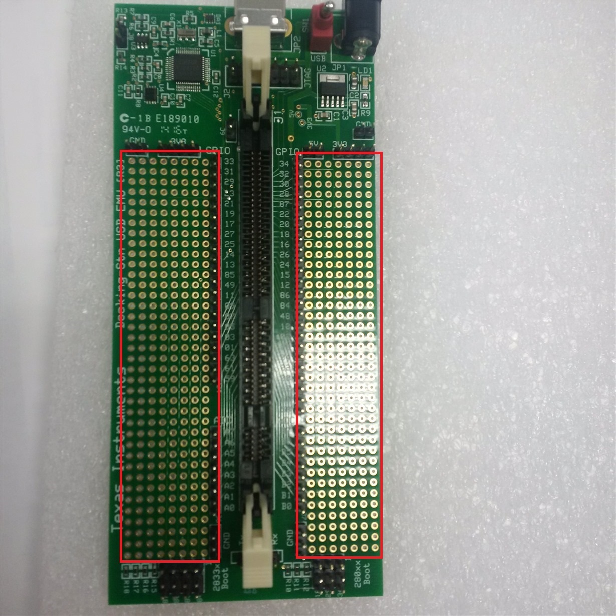
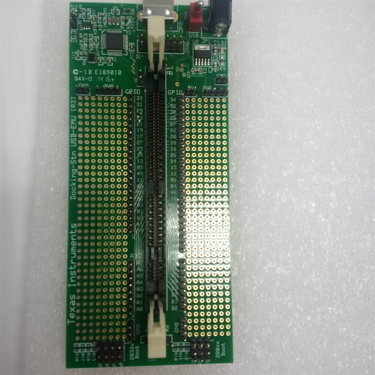
Which is pin 1 and pin 2 (of the solder-able part of the docking station) so that I can figure out all pin allocations from control suite schematic). Please draw two arrows to indicate pin 1 and pin 2 in photo provided.
This thread has been locked.
If you have a related question, please click the "Ask a related question" button in the top right corner. The newly created question will be automatically linked to this question.
Which is pin 1 and pin 2 (of the solder-able part of the docking station) so that I can figure out all pin allocations from control suite schematic). Please draw two arrows to indicate pin 1 and pin 2 in photo provided.
Amit,
I do not completely understand what you are asking.
However, you can find the Docking Station (the controlCARD's baseboard) at the below link (assuming you have controlSUITE installed):
\controlSUITE\development_kits\~ExperimentersKits\ExperimentersKit-HWdevPkg\USBDockingStation_Schematic [R3].pdf
Note that the pin numbering of J1 corresponds to the numbering in the "controlCARD-DIMM100-PinPositions.ppt" document you referred to.
The usage of J4-J7 is also shown. For example, J1.pin95 will go to J4.pin1. J4 pin 1 is labelled as "33" in the silkscreen of the PCB.
Hopefully this helps.
Thank you,
Brett