This thread has been locked.

If you have a related question, please click the "Ask a related question" button in the top right corner. The newly created question will be automatically linked to this question.

TMS320F28377S ADC window comparator interrupts

Other Parts Discussed in Thread: CONTROLSUITE, TMS320F28377S

Hi,

Need help setting up the TMS320F2837x  one of the four 16 bit ADCs to perform continuous conversions and trigger an interrupt once a window high/low comparator level has been exceeded.

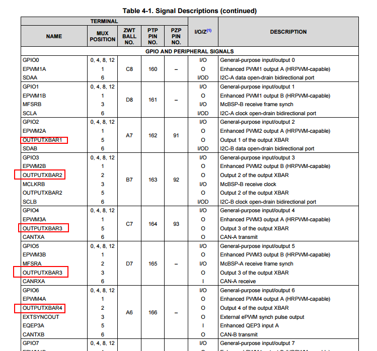
I guess my main Challenger since  im new to the CPU is the PinMux. I played with  the PinMux utility but it does not cover advance ADC stuff  in much detail.

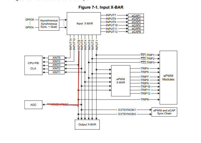
I am not quite sure how the INPUTXBAR and OUTPUTXBAR play into this. For now I just need to get the basic ADC running of which there seem to be plenty of examples.

However the tricky part is connecting the window comparator to the ADC channel, setting comparator setpoints and somehow get it to generate interrupts. The other challenge is how to trace the control flag registers to be able to know the source of the interrupt e.g. which adc channel and what level etc.  And then there is the XBAR which I have not quite got my head wrapped arround  +1000 pages of data sheets.

Anyhow I am trying to get as much out of this forum to speed up the learning curve - please bare with me. 

I have the development system setup and running using the Launchpad. Can download and debug the examples.

Code snippeds and suggestions would be greatly welcomed just to get me started in the shortest amount of time

Thanks

Nick Amos

  • Hi Nick,

    There are actually two options here:
    -Use the analog comparator + DAC to generate a trip when the voltage is outside of the specified range. The resolution here is 12-bits (for the comparator DAC), but the trip is pretty fast, probably < 100ns
    -Use the ADC sampling continuously in 16-bit mode + the PPB to generate an interrupt when the voltage is outside of the given range. The resolution here is 16-bits, but the time from over/under voltage event to trip is more like 1us

    I think you want to do the second case, so
    (1)Get the ePWM sampling example to work on the channel of interest (I think you want this and not continuous conversions because the PPB only works on a single SOC at a time). The ADC channels don't have any muxing; there is only one option for a given ADC channel (actually a channel pair in 16-bit mode, since the input is differential).
    (2a) Decrease ePWM period so that a trigger is generated at ~1MHz instead of whatever is in the example
    (2b) Remove the ADC interrupt - you won't need to read the ADC results directly
    (3) Point one of the ADC PPBs at the SOC you are using (probably SOC0) and set the high and low limits to whatever you want. You can read the PPB high/low trip flags directly to see if the signal is going outside the limits.
    (4)Enable the PPB event interrupt for the PPB you are using both in the ADC and in the PIE. Each PPB interrupt has a dedicated PIE vector, so you will know where the interrupt is coming from based on the ISR you choose to handle the PPB interrupt.
  • Hi Devin,

    Thanks for the quick response. The analog comparator + DAC certainly seems very enticing. I initially designed the hardware to have this function available outside the CPU using one of the CPU 12 bit DACs. However if this can be done inside the CPU i certainly would like to try that first.

    Do you perhaps know which sample code might show how to setup this arrangment - e.g. control registers and/if the XBAR needs to be utilized. As you might have noticed, i am *** scared of the XBAR complexity, it looks very intimidating.
  • Hi Nick,

    If you want to use the internal comparators, you should look at documentation for the 'CMPSS' module. In this case, if you want an interrupt, you will need to use the XBARs since the CMPSS can't generate an interrupt directly. In this case, you need to do 2 things (in addition to configuring the CMPSS): (1) Setup the output crossbar to put the CMPSS output trip on a pin. (2) Setup the input crossbar to generate an interrupt from the same pin. In the case of the output X-BAR, the X-BAR isn't really anything more than a big mux, you just need to figure out the right selection for CMPSSx trip. For the input XBAR, it is also just a big mux that can select all of the GPIOs. So if you want GPIO10 you write '10' to the crossbar select.

    As far as an example, take a look at the cmpss_asynch example in ControlSUITE. This will get the comparator signal as far as the output pin.
  • Hi Devin,

    OK Devin this is pretty much what i suspected after a quick look at the data sheets - many moons ago. Anyhow I  need to produce a circuit board and it seems to me that its gonna be too premature to try map the physical controller pins to the PCB since I am not sure how the CMPSS and XBAR is going to pan out thats why i intinially decided to do the comparator externally....haha

    Can you possibly provide me with a sample project derrived from the  "cmpss_asynch" example project

    showing how the XBAR is used to generate an interrupt from the CMPSS analog input. That would be really appreciated

    Thanks

    .

  • Nick,

    Here's a copy of "cmpss_asynch" with some code snippets ported over from "external_interrupt" to enable GPIO interrupts using the comparator output pin.

    //###########################################################################
    // FILE:   cmpss_digital_filter_cpu01.c
    // TITLE:  CMPSS Digital Filter Example Configuration for F2837xS.
    //
    //! \addtogroup cpu01_example_list
    //! <h1> CMPSS Asynchronous Trip </h1>
    //!
    //! This example enables the CMPSS1 COMPH comparator and feeds the asynch
    //! CTRIPOUTH to GPIO14/OUTPUTXBAR3 pin and CTRIPH to GPIO15/EPWM8B
    //!
    //! The COMPH inputs are:
    //!   -  POS signal from CMPIN1P pin
    //!   -  NEG signal from internal DACH
    //!
    //
    //###########################################################################
    // $TI Release: F2837xS Support Library v191 $
    // $Release Date: Fri Mar 11 15:58:35 CST 2016 $
    // $Copyright: Copyright (C) 2014-2016 Texas Instruments Incorporated -
    //             http://www.ti.com/ ALL RIGHTS RESERVED $
    //###########################################################################
    
    #include "F28x_Project.h"     // Device Headerfile and Examples Include File
    
    // Prototype statements for functions found within this file.
    interrupt void xint1_isr(void);
    
    // Global variables for this example
    volatile Uint32 Xint1Count = 0;
    
    //definitions for selecting DACH reference
    #define REFERENCE_VDDA     0
    #define REFERENCE_VDAC     1
    
    //definitions for COMPH input selection
    #define NEGIN_DAC          0
    #define NEGIN_PIN          1
    
    //definitions for CTRIPH/CTRIPOUTH output selection
    #define CTRIP_ASYNCH       0
    #define CTRIP_SYNCH        1
    #define CTRIP_FILTER       2
    #define CTRIP_LATCH        3
    
    //definitions for selecting output pin
    #define GPIO_CTRIP_PIN_NUM      14 //OUTPUTXBAR3 is mux'd with GPIO14
    #define GPIO_CTRIP_PER_NUM       6 //OUTPUTXBAR3 is peripheral option 6 for GPIO14
    #define GPIO_CTRIPOUT_PIN_NUM   15 //EPWM8B is mux'd with GPIO15
    #define GPIO_CTRIPOUT_PER_NUM    1 //EPWM8B is peripheral option 1 for GPIO15
    
    void InitCMPSS(void);
    void InitEPWM(void);
    
    void main(void)
    {
    // Step 1. Initialize System Control:
    // PLL, WatchDog, enable Peripheral Clocks
    // This example function is found in the F2837xS_SysCtrl.c file.
        InitSysCtrl();
    
    // Step 2. Initialize GPIO:
    // This example function is found in the F2837xS_Gpio.c file and
    // illustrates how to set the GPIO to it's default state.
        InitGpio();
        
    // Step 3. Clear all interrupts and initialize PIE vector table:
    // Disable CPU interrupts
        DINT;
    
    // Initialize the PIE control registers to their default state.
    // The default state is all PIE interrupts disabled and flags
    // are cleared.
    // This function is found in the F2837xS_PieCtrl.c file.
        InitPieCtrl();
    
    // Disable CPU interrupts and clear all CPU interrupt flags:
        IER = 0x0000;
        IFR = 0x0000;
    
        InitPieVectTable();
    
     // Interrupts that are used in this example are re-mapped to
     // ISR functions found within this file.
        EALLOW;  // This is needed to write to EALLOW protected registers
        PieVectTable.XINT1_INT = &xint1_isr;
        EDIS;   // This is needed to disable write to EALLOW protected registers
    
     // Enable XINT1 and XINT2 in the PIE: Group 1 interrupt 4 & 5
     // Enable INT1 which is connected to WAKEINT:
        PieCtrlRegs.PIECTRL.bit.ENPIE = 1;          // Enable the PIE block
        PieCtrlRegs.PIEIER1.bit.INTx4 = 1;          // Enable PIE Group 1 INT4
        IER |= M_INT1;                              // Enable CPU INT1
        PieCtrlRegs.PIEACK.all = PIEACK_GROUP1;
        EINT;
    
    // Configure Comparator COMP1H to accept POS input from pin and NEG input from DAC
        InitCMPSS();
    // Configure COMP1 to feed TRIP4 EPWM DC trip input
        InitEPWM();
    
    // Configure GPIO15 to output CTRIP1H/EPWM TRIP4
        GPIO_SetupPinMux(   GPIO_CTRIP_PIN_NUM, GPIO_MUX_CPU1,    GPIO_CTRIP_PER_NUM);
    // Configure GPIO14 to output CTRIPOUT1H
        GPIO_SetupPinMux(GPIO_CTRIPOUT_PIN_NUM, GPIO_MUX_CPU1, GPIO_CTRIPOUT_PER_NUM);
    
        GpioCtrlRegs.GPAQSEL1.bit.GPIO14 = 2;       // XINT1 Qual using 6 samples
        GpioCtrlRegs.GPACTRL.bit.QUALPRD1 = 0xFF;   // Each sampling window is 510*SYSCLKOUT
    
        GPIO_SetupXINT1Gpio(14);
    
     // Configure XINT1
        XintRegs.XINT1CR.bit.POLARITY = 1;      // Rising edge interrupt
    
     // Enable XINT1
        XintRegs.XINT1CR.bit.ENABLE = 1;        // Enable XINT1
    
        while(1) 
        {
            // Trip flags set when CTRIP signal is asserted
            if( EPwm8Regs.TZFLG.bit.OST ) 
            {
                EALLOW;
                // Wait for comparator CTRIP to de-assert
                while( Cmpss1Regs.COMPSTS.bit.COMPHSTS );
                // Clear trip flags
                EPwm8Regs.TZCLR.bit.OST     = 1;
                EPwm8Regs.TZCLR.bit.INT     = 1;
                EDIS;
            }
        }
    }
    
    interrupt void xint1_isr(void)
    {
        Xint1Count++;
    
        // Acknowledge this interrupt to get more from group 1
        PieCtrlRegs.PIEACK.all = PIEACK_GROUP1;
    }
    
    void InitCMPSS(void) 
    {
        EALLOW;
        //Enable CMPSS
        Cmpss1Regs.COMPCTL.bit.COMPDACE            = 1;
        //NEG signal comes from DAC
        Cmpss1Regs.COMPCTL.bit.COMPHSOURCE         = NEGIN_DAC;
        //Use VDDA as the reference for DAC
        Cmpss1Regs.COMPDACCTL.bit.SELREF           = REFERENCE_VDDA;
        //Set DAC to midpoint for arbitrary reference
        Cmpss1Regs.DACHVALS.bit.DACVAL             = 2048;
    
    // Configure CTRIPOUT path
        //Asynch output feeds CTRIPH and CTRIPOUTH
        Cmpss1Regs.COMPCTL.bit.CTRIPHSEL           = CTRIP_ASYNCH;
        Cmpss1Regs.COMPCTL.bit.CTRIPOUTHSEL        = CTRIP_ASYNCH;
    
        Cmpss1Regs.COMPHYSCTL.bit.COMPHYS          = 4; // Enable hysteresis
    
    // Configure CTRIPOUTH output pin
        //Configure OUTPUTXBAR3 to be CTRIPOUT1H
        OutputXbarRegs.OUTPUT3MUX0TO15CFG.bit.MUX0 = 0;
        //Enable OUTPUTXBAR3 Mux for Output
        OutputXbarRegs.OUTPUT3MUXENABLE.bit.MUX0   = 1;
        EDIS;
    }
    
    void InitEPWM(void) 
    {
        EALLOW;
        CpuSysRegs.PCLKCR0.bit.TBCLKSYNC       = 0;
    
        //Configure EPWM to run at SYSCLK
        ClkCfgRegs.PERCLKDIVSEL.bit.EPWMCLKDIV = 0;
        EPwm8Regs.TBCTL.bit.CLKDIV             = 0;
        EPwm8Regs.TBCTL.bit.HSPCLKDIV          = 0;
        //Initialize dummy values for EPWM CTR/PRD
        EPwm8Regs.TBCTR                        = 0;
        EPwm8Regs.TBPRD                        = 0xFFFF;
    
        //Configure EPWM8B to output high on TZB TRIP
        EPwm8Regs.TZCTL.bit.TZB                = TZ_FORCE_HI;
        //Configure DCB to be TRIP4
        EPwm8Regs.TZDCSEL.bit.DCBEVT1          = TZ_DCBH_HI;
        EPwm8Regs.DCTRIPSEL.bit.DCBHCOMPSEL    = 0xF; //DCBHTRIPSEL
        EPwm8Regs.DCBHTRIPSEL.bit.TRIPINPUT4   = 1;
        //Configure DCB as OST
        EPwm8Regs.TZSEL.bit.DCBEVT1            = 1;
        //Configure DCB path to be unfiltered & async
        EPwm8Regs.DCBCTL.bit.EVT1SRCSEL        = DC_EVT1;
        EPwm8Regs.DCBCTL.bit.EVT1FRCSYNCSEL    = DC_EVT_ASYNC;
    
        CpuSysRegs.PCLKCR0.bit.TBCLKSYNC       = 1;
    
        //Configure TRIP4 to be CTRIP1H
        EPwmXbarRegs.TRIP4MUX0TO15CFG.bit.MUX0 = 0;
        //Enable TRIP4 Mux for Output
        EPwmXbarRegs.TRIP4MUXENABLE.bit.MUX0   = 1;
    
        // Clear trip flags
        EPwm8Regs.TZCLR.bit.OST                = 1;
        EPwm8Regs.TZCLR.bit.INT                = 1;
        //Enable DCB interrupt
        EPwm8Regs.TZEINT.bit.OST               = 1;
    
        // Enable PWM
        EPwm8Regs.TBCTL.bit.CTRMODE            = TB_COUNT_UP;
    
        EDIS;
    }
    

    -Tommy

  • OK so I tried the modified example kindly provided by Tommy - however I am still not out of the woods....

    What I am attempting to do is to connect single ended ADC 12 bit compare high outputs to the Output XBAR to any GPIO pins that support muxing to the CMPSS blocks on the 28377S in order to map these outputs for PCB layout. I have pretty much mapped out the complete chip and its resources, however I cannot succesfully map the CMPSS compare high to the Output XBAR - I need help .....HELP!!

    I am using the example provided by Tommy. However - I do not need the EPWM stuff. I do not use PWM for this project. I simply need to compare analog inputs and trigger interrupts on ADC channels as fast as possible.

    All the example code for CMPSS comparators only explain how to connect one comparator. I need to connect them all - and I am unable to replicate the example to include more comparators to external pins - never mind interrupts. At this stage I just need to observe with my scope probe the switching outputs of each comparator pin.

    Could someone please assist with this problem.

    Thanks

    Nick


    I noticed that  the cmpss exampl

  • Hi Nick,

    To get the CMPSS outputs to a pin, use the output x-bar.  For a give output x-bar, you just need to make the following selection:

    Once you have made the selection for a given output XBAR, you can get it to the pin by changing the GPIO mux for a pin that has that output XBAR:


    Now you should be able to observe it on the pin.  To trigger the ADC, there is a singe input XBAR that you can configure:

    This configuration is as easy as picking whatever GPIO you want:

    In the ADC SOC configuration logic, you would write '4' to the trigger select to use this as the trigger.

    Note that the output XBARs have a big OR gate in them, so you could use multiple CMPSS modules to cause the same ADC trigger, but you can't get multiple CMPSS modules to generate different ADC triggers.


    Now if you want to generate an interrupt instead of triggering the ADC, use input Xbars 14, 13, 6, 5, or 4.

  • Regarding the 100 pin TMS320F28377S package and the OUTPUT XBAR. It was interesting to note that even though some GPIOs were not available external to the chip, I still managed to map these pins internally via the GPIO mux to interrupts coming from the CMPSS comparator outputs - that is encouraging.....

    However this is just playing with the first instance of the comparator structure elements as provided in the above mentioned examples. I tried to cut 'n paste, twiddle settings but were unable to duplicate the comparator example for cmpss(1) onto additional comparators -

    However I am able to map the first comparator to any of the OUTPUT XBAR and generate interrupts - that part I seems to have figured out.
  • Devin,

    I have opted to not use the ADC window triggers since you mentioned how slow the propagation turns out to be. In stead I am wanting to map the CMPSS comparators - as you know the comparators only share the IO pin with the ADCs in question.

    So mapping the CMPSS to IO pins and then as a secondary effort to interrupts. I am unsing the support libraries provided by TI and would like to stay within the C/C++ abstraction of the registers. If i start to address registers directly I am surely going to break the code using the support libraries at some point.

    That said - I wish to see some sample code replicating the CMPSS comparators for more than one ADC channel using the the helper code libraries as used in the cmpss examples. Can you demonstrate that for me please?
  • Nick,

    I noticed a mismatch in the comment statements / #define names in the example code with respect to the GPIO14 and GPIO15 MUX settings.  I hope that isn't throwing you off.

    Here's a breakdown of the key configurations.  Hopefully it helps.

    -Tommy

  • OK I have it working now  - the problem seems to be resolved - thank you all very much........for now....


    void InitCMPSS1(void);
    void InitCMPSS2(void);
    void InitCMPSS3(void);
    void InitCMPSS4(void);

    void main(void)
    {
    // Step 1. Initialize System Control:
    // PLL, WatchDog, enable Peripheral Clocks
    // This example function is found in the F2837xS_SysCtrl.c file.
    InitSysCtrl();

    // Step 2. Initialize GPIO:
    // This example function is found in the F2837xS_Gpio.c file and
    // illustrates how to set the GPIO to it's default state.
    InitGpio();

    // Step 3. Clear all interrupts and initialize PIE vector table:
    // Disable CPU interrupts
    DINT;

    // Initialize the PIE control registers to their default state.
    // The default state is all PIE interrupts disabled and flags
    // are cleared.
    // This function is found in the F2837xS_PieCtrl.c file.
    InitPieCtrl();

    // Disable CPU interrupts and clear all CPU interrupt flags:
    IER = 0x0000;
    IFR = 0x0000;

    InitPieVectTable();

    InitCMPSS1(); // route XBAR 7 to GPIO 16 on ADC_A2: CMPIN1P
    InitCMPSS2(); // route XBAR 3 to GPIO 14 on ADC_A4: CMPIN2P
    InitCMPSS3(); // route XBAR 1 to GPIO   2 on ADC_B2: CMPIN3P
    InitCMPSS4(); // route XBAR 4 to GPIO 15 on ADC_14: CMPIN4P

    GPIO_SetupPinMux(16,0,3);// XBAR 7  to ADC_A2

    GPIO_SetupPinMux(14,0,6);// XBAR 3 to ADC_A4

    GPIO_SetupPinMux(2,0,5);  // XBAR 1 to ADC_B2

    GPIO_SetupPinMux(15,0,6);// XBAR 4 to ADC_14

    while(1)
    {

    // do nothing  - idle

    }
    }

    void InitCMPSS1(void)
    {
    EALLOW;
    //Enable CMPSS
    Cmpss1Regs.COMPCTL.bit.COMPDACE = 1;
    //NEG signal comes from DAC
    Cmpss1Regs.COMPCTL.bit.COMPHSOURCE = NEGIN_DAC;
    //Use VDDA as the reference for DAC
    Cmpss1Regs.COMPDACCTL.bit.SELREF = REFERENCE_VDDA;
    //Set DAC to midpoint for arbitrary reference
    Cmpss1Regs.DACHVALS.bit.DACVAL = 2048;

    // Configure CTRIPOUT path
    //Asynch output feeds CTRIPH and CTRIPOUTH
    Cmpss1Regs.COMPCTL.bit.CTRIPHSEL = CTRIP_ASYNCH;
    Cmpss1Regs.COMPCTL.bit.CTRIPOUTHSEL = CTRIP_ASYNCH;

    Cmpss1Regs.COMPHYSCTL.bit.COMPHYS = 4; // Enable hysteresis

    // Configure CTRIPOUTH output pin

    OutputXbarRegs.OUTPUT7MUX0TO15CFG.bit.MUX0 = 0;

    //Enable OUTPUTXBAR3 Mux for Output
    OutputXbarRegs.OUTPUT7MUXENABLE.bit.MUX0 = 1;
    EDIS;
    }

    void InitCMPSS2(void)
    {
    EALLOW;
    //Enable CMPSS
    Cmpss2Regs.COMPCTL.bit.COMPDACE = 1;
    //NEG signal comes from DAC
    Cmpss2Regs.COMPCTL.bit.COMPHSOURCE = NEGIN_DAC;
    //Use VDDA as the reference for DAC
    Cmpss2Regs.COMPDACCTL.bit.SELREF = REFERENCE_VDDA;
    //Set DAC to midpoint for arbitrary reference
    Cmpss2Regs.DACHVALS.bit.DACVAL = 2048;//1000;

    // Configure CTRIPOUT path
    //Asynch output feeds CTRIPH and CTRIPOUTH
    Cmpss2Regs.COMPCTL.bit.CTRIPHSEL = CTRIP_ASYNCH;
    Cmpss2Regs.COMPCTL.bit.CTRIPOUTHSEL = CTRIP_ASYNCH;

    Cmpss2Regs.COMPHYSCTL.bit.COMPHYS = 4; // Enable hysteresis

    // Configure CTRIPOUTH output pin

    OutputXbarRegs.OUTPUT3MUX0TO15CFG.bit.MUX2 = 0;

    //Enable OUTPUTXBAR3 Mux for Output
    OutputXbarRegs.OUTPUT3MUXENABLE.bit.MUX2 = 1;
    EDIS;
    }


    void InitCMPSS3(void)
    {
    EALLOW;
    //Enable CMPSS
    Cmpss3Regs.COMPCTL.bit.COMPDACE = 1;
    //NEG signal comes from DAC
    Cmpss3Regs.COMPCTL.bit.COMPHSOURCE = NEGIN_DAC;
    //Use VDDA as the reference for DAC
    Cmpss3Regs.COMPDACCTL.bit.SELREF = REFERENCE_VDDA;
    //Set DAC to midpoint for arbitrary reference
    Cmpss3Regs.DACHVALS.bit.DACVAL = 2048;//1000;

    // Configure CTRIPOUT path
    //Asynch output feeds CTRIPH and CTRIPOUTH
    Cmpss3Regs.COMPCTL.bit.CTRIPHSEL = CTRIP_ASYNCH;
    Cmpss3Regs.COMPCTL.bit.CTRIPOUTHSEL = CTRIP_ASYNCH;

    Cmpss3Regs.COMPHYSCTL.bit.COMPHYS = 4; // Enable hysteresis

    // Configure CTRIPOUTH output pin

    OutputXbarRegs.OUTPUT1MUX0TO15CFG.bit.MUX4 = 0;

    //Enable OUTPUTXBAR3 Mux for Output
    OutputXbarRegs.OUTPUT1MUXENABLE.bit.MUX4 = 1;
    EDIS;
    }


    void InitCMPSS4(void)
    {
    EALLOW;
    //Enable CMPSS
    Cmpss4Regs.COMPCTL.bit.COMPDACE = 1;
    //NEG signal comes from DAC
    Cmpss4Regs.COMPCTL.bit.COMPHSOURCE = NEGIN_DAC;
    //Use VDDA as the reference for DAC
    Cmpss4Regs.COMPDACCTL.bit.SELREF = REFERENCE_VDDA;
    //Set DAC to midpoint for arbitrary reference
    Cmpss4Regs.DACHVALS.bit.DACVAL = 2048;//1000;

    // Configure CTRIPOUT path
    //Asynch output feeds CTRIPH and CTRIPOUTH
    Cmpss4Regs.COMPCTL.bit.CTRIPHSEL = CTRIP_ASYNCH;
    Cmpss4Regs.COMPCTL.bit.CTRIPOUTHSEL = CTRIP_ASYNCH;

    Cmpss4Regs.COMPHYSCTL.bit.COMPHYS = 4; // Enable hysteresis

    // Configure CTRIPOUTH output pin


    OutputXbarRegs.OUTPUT4MUX0TO15CFG.bit.MUX6 = 0;

    //Enable OUTPUTXBAR3 Mux for Output

    OutputXbarRegs.OUTPUT4MUXENABLE.bit.MUX6 = 1;
    EDIS;
    }