


Hello,
I'm trying create a program that generate a SOC pulse to trigger an ADC conversion. I want to use the Digital Compare submodule to generate the SOC pulse, for this i'm using the comparator with the internal DAC to produce the DC event.
I don't understand that is wrong in my code, because the conversion not is generated, in other words the SOC pulse don't is created.
My ePWM2 configuration:
void Config_EPwm2(void)
{
// Initialize GPIO
GPIO_setPullUp(myGpio, GPIO_Number_2, GPIO_PullUp_Disable);
GPIO_setPullUp(myGpio, GPIO_Number_3, GPIO_PullUp_Disable);
GPIO_setMode(myGpio, GPIO_Number_2, GPIO_2_Mode_EPWM2A);
GPIO_setMode(myGpio, GPIO_Number_3, GPIO_3_Mode_EPWM2B);
CLK_enablePwmClock(myClk, PWM_Number_2);
PWM_setClkDiv(myPwm2,PWM_ClkDiv_by_128); // (TB)-TBCLK) 60.000.000/128 = 468.750kHz
PWM_setPeriod(myPwm2, 0xFFFF); // (TB)-0xFFFF = 65535 ---> 468.750/65533 = 7.15Hz
PWM_setCounterMode(myPwm2, PWM_CounterMode_UpDown); // (TB)-Count Up and Down --> 7.15/2 = 3.57Hz
PWM_setSyncMode(myPwm2, PWM_SyncMode_EPWMxSYNC); // (TB) Setup Sync
PWM_enableCounterLoad(myPwm2); // (TB) (SLAVE module) Enable phase loading
//PWM_disableCounterLoad(myPwm2); // (TB) (MASTER module) Disable phase loading
PWM_setPhase(myPwm2, 40000); // (TB) Set phase value
PWM_setPhaseDir(myPwm2,PWM_PhaseDir_CountUp); // (TB) Define direção de contagem crescente, após carregar valor de fase
PWM_setShadowMode_CmpA(myPwm2, PWM_ShadowMode_Shadow); // (CC) Content of the shadow register is transferred to the active register on one of the
PWM_setShadowMode_CmpB(myPwm2,PWM_ShadowMode_Shadow); // (CC) following events as specified by the CMPCTL[LOADAMODE] and CMPCTL[LOADBMODE] register bits.
PWM_setLoadMode_CmpA(myPwm2, PWM_LoadMode_Zero); // (CC) Load COMPA on CTR=Zero event (transfer the content in shadow register to COMPA)
PWM_setLoadMode_CmpB(myPwm2, PWM_LoadMode_Zero); // (CC)
PWM_setActionQual_CntUp_CmpA_PwmA(myPwm2,PWM_ActionQual_Set); // (AQ) set actions for EPWM1A
PWM_setActionQual_CntDown_CmpA_PwmA(myPwm2,PWM_ActionQual_Clear); // (AQ)
PWM_setActionQual_CntUp_CmpB_PwmB(myPwm2,PWM_ActionQual_Set); // (AQ) set actions for EPWM1B
PWM_setActionQual_CntDown_CmpB_PwmB(myPwm2,PWM_ActionQual_Clear); // (AQ)
PWM_setIntMode(myPwm2, PWM_IntMode_CounterEqualPeriod); // (ET&I) ETSEL[INTSEL], Enable INT on Zero event
PWM_enableInt(myPwm2); // (ET&I) ETSEL[INTEN], Enable INT
PWM_setIntPeriod(myPwm2, PWM_IntPeriod_ThirdEvent); // (ET&I) ETPS[INTPRD], Generate INT on 2nd event
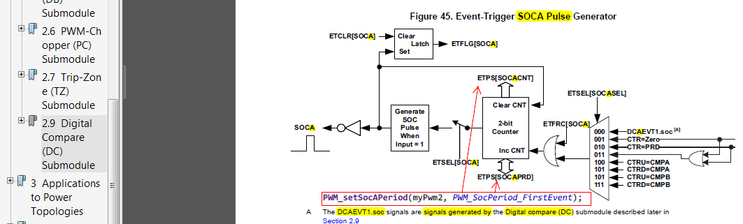
PWM_enableSocAPulse(myPwm2); // (ET&I) ETSEL[SOCAEN], Habilita/permite pulsos SocA.
PWM_setSocAPulseSrc(myPwm2,PWM_SocPulseSrc_DcEvt); // (ET&I) ETSEL[SOCASEL], Fonte que gera o pulso SocA (Enable DCAEVT1.soc event), sinal gerado pelo (DC) -Digital Compare
PWM_setSocAPeriod(myPwm2, PWM_SocPeriod_FirstEvent); // (ET&I) ETPS[SOCAPRD], Gerar o pulso na 1ª ocurrencia da fonte do evento
// Define an event (DCAEVT1) baseado em COMP1OUT e TZ2
PWM_setDigitalCompareInput(myPwm2,PWM_DigitalCompare_A_High,PWM_DigitalCompare_InputSel_COMP1OUT); // (DC) DCTRIPSEL[DCAHCOMPSEL], DCAH = COMP1OUT
PWM_setDigitalCompareInput(myPwm2,PWM_DigitalCompare_A_Low,PWM_DigitalCompare_InputSel_TZ2); // (DC) DCTRIPSEL[DCALCOMPSEL], DCAL = TZ2 (**)
PWM_setTripZoneDCEventSelect_DCAEVT1(myPwm2, PWM_TripZoneDCEventSel_DCxHH_DCxLX); // (DC) TZDCSEL[DCAEVT1], DCAEVT1 = (DCAH (Compare H = High, Ativo quando a saída COMP1OUT for a nível alto "1")), (Compare L = Não faz nada/ não importa)(**)
PWM_setDigitalCompareAEvent1(myPwm2, false, false, true, false); // (DC) DCACTL[], DCAEVT1 = DCAEVT1(não filtrado), usa caminho Sync (sincronizado), activa a geração do sinal soc, não gera sinal de sincronização.
PWM_setCmpA(myPwm2,10383); // (CC) -adjust duty for output EPWM1A -GPIO0
PWM_setCmpB(myPwm2,32766); // (CC) -adjust duty for output EPWM1B -GPIO1
}
If possible can someone confirm me if the code lines 32 to 40 is correct to configure the Digital Compare for generate a pulse SOCA?

My Comp1 configuration:
void Config_Comp1(void)
	{
	//GPIO_setMode(myGpio, GPIO_Number_1, GPIO_1_Mode_COMP1OUT);	//Para fazer sair no pino o estado da saida do comparador

    //ADC_enableBandGap(myAdc);									// 1ºpasso (da inicialização) Configured in the ADC configution.
    COMP_enable(myComp1);										// 2ºpasso (da inicialização) Power up Comparator 1 locally
    COMP_enableDac(myComp1);									// Entrada inversora do comparador conectada ao DAC interno
    COMP_selectDacSrc(myComp1, COMP_DacSrc_DacValue);		// Select the souce to control the DAC ("COMP_DacSrc_RampGenerator" ou "COMP_DacSrc_DacValue").
    COMP_setDacValue(myComp1, 512);							// Set DAC output to midpoint
}
If possible can someone confirm me if the code is correct to set comparator to use the COMP1A input and the output of the internal DAC, as input signals?
Note: When I run the program we place 3.3v voltage at COMP1A pin (Input Pin A).

My ADC configuration:
void Config_ADC_and_interrupt(void)
	{
    PIE_registerPieIntHandler(myPie, PIE_GroupNumber_10, PIE_SubGroupNumber_1,(intVec_t)&adc_ISR);		// Register interrupt handlers in the PIE vector table
    PIE_registerPieIntHandler(myPie, PIE_GroupNumber_10, PIE_SubGroupNumber_2,(intVec_t)&adc_ISR_2);	// Register interrupt handlers in the PIE vector table

    // Initialize the ADC
    ADC_enableBandGap(myAdc);							// Enables the ADC band gap circuit
    ADC_enableRefBuffers(myAdc);						// Enables the ADC reference buffers circuit
    ADC_powerUp(myAdc);									// Powers up the ADC
    ADC_enable(myAdc);									// Enables the ADC
    ADC_setVoltRefSrc(myAdc, ADC_VoltageRefSrc_Int);	// Sets the voltage reference source (0-3.3V)


    //********************************************** Configurar ADCINT2 ****************************************************************
    //O canal ADCINA4 será duplamente amostrado para resolver a questão da primeira amostra ADC, errata rev0 silício
    ADC_setSocTrigSrc(myAdc, ADC_SocNumber_2, ADC_SocTrigSrc_EPWM2_ADCSOCA);   	 	// set SOC0 start trigger on EPWM2A, due to round-robin SOC0 converts first then SOC1
    ADC_setSocTrigSrc(myAdc, ADC_SocNumber_3, ADC_SocTrigSrc_EPWM2_ADCSOCA);   	 // Configura o disparo de conersão SOC1 controlado por EPWM2A, devido ao round-robin converte primeiro SOC0 e depois SOC1
    ADC_setSocChanNumber(myAdc, ADC_SocNumber_2, ADC_SocChanNumber_A6);    			 // set SOC2 channel select to ADCINA6 (localizado 1 pino do "pente" J1, na placa)
    ADC_setSocChanNumber(myAdc, ADC_SocNumber_3, ADC_SocChanNumber_A6);    			 // Define canal selecionado pelo SOC1, para ADCINA4
    ADC_setSocSampleWindow(myAdc, ADC_SocNumber_2, ADC_SocSampleWindow_64_cycles);   // set SOC0 S/H Window to 64 ADC Clock Cycles, (63 ACQPS more 1)
    ADC_setSocSampleWindow(myAdc, ADC_SocNumber_3, ADC_SocSampleWindow_64_cycles);   // set SOC1 S/H Window to 64 ADC Clock Cycles, (63 ACQPS more 1)

    // Configure ADC interrupt
    ADC_setIntPulseGenMode(myAdc, ADC_IntPulseGenMode_Prior);               // Gerar o pulso interrupção (ADCINT2) um ciclo antes de trancar/terminar o resultado ADC (AdcResults).
    ADC_enableInt(myAdc, ADC_IntNumber_2);                                  // Enabled interrupt "ADCINT2"
    ADC_setIntMode(myAdc, ADC_IntNumber_2, ADC_IntMode_ClearFlag);          // Disable ADCINT2 Continuous mode, a new interrupt not be generated until the interrupt flag is cleared.
    ADC_setIntSrc(myAdc, ADC_IntNumber_2, ADC_IntSrc_EOC3);                 // Configura EOC2 (End of conversion) para disparar ADCINT2.
    PIE_enableAdcInt(myPie, ADC_IntNumber_2);						// Enable ADCINT2 in PIE: Group 10 interrupt 2

    CPU_enableInt(myCpu, CPU_IntNumber_10);				// Enable CPU INT10 (Interrupt 10) which is connected to ADCINT1
	}
