This thread has been locked.

If you have a related question, please click the "Ask a related question" button in the top right corner. The newly created question will be automatically linked to this question.

TMS320F28377D Emif

Other Parts Discussed in Thread: TMS320F28335

Hi, 

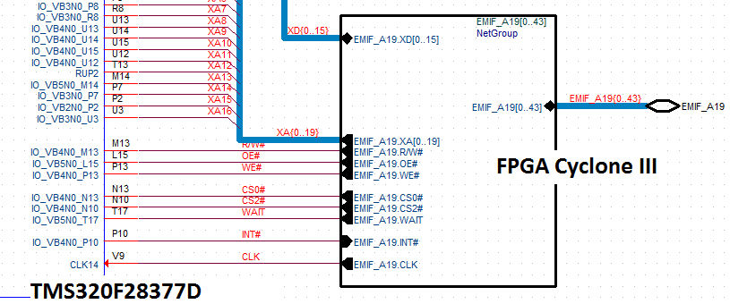
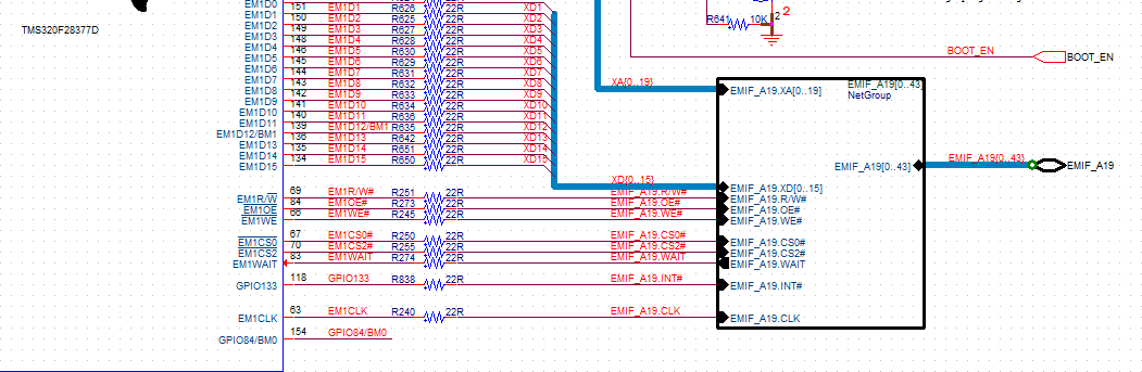
I am using TMS320F28377D, configuring the EMIF1 to interface FPGA(CYCLONE III). While  working  using controlSuite example EMIF1_16bit_ASRAM :

 The config Emif1 as 16 bits data follow in example (without changes): 

//Configure the access timing for CS2 space
Emif1Regs.ASYNC_CS2_CR.all = (EMIF_ASYNC_ASIZE_16 | // 16Bit Memory Interface
EMIF_ASYNC_TA_1 | // Turn Around time of 2 Emif Clock
EMIF_ASYNC_RHOLD_1 | // Read Hold time of 1 Emif Clock
EMIF_ASYNC_RSTROBE_4 | // Read Strobe time of 4 Emif Clock
EMIF_ASYNC_RSETUP_1 | // Read Setup time of 1 Emif Clock
EMIF_ASYNC_WHOLD_1 | // Write Hold time of 1 Emif Clock
EMIF_ASYNC_WSTROBE_1 | // Write Strobe time of 1 Emif Clock
EMIF_ASYNC_WSETUP_1 | // Write Setup time of 1 Emif Clock
EMIF_ASYNC_EW_DISABLE | // Extended Wait Disable.
EMIF_ASYNC_SS_DISABLE // Strobe Select Mode Disable.
);

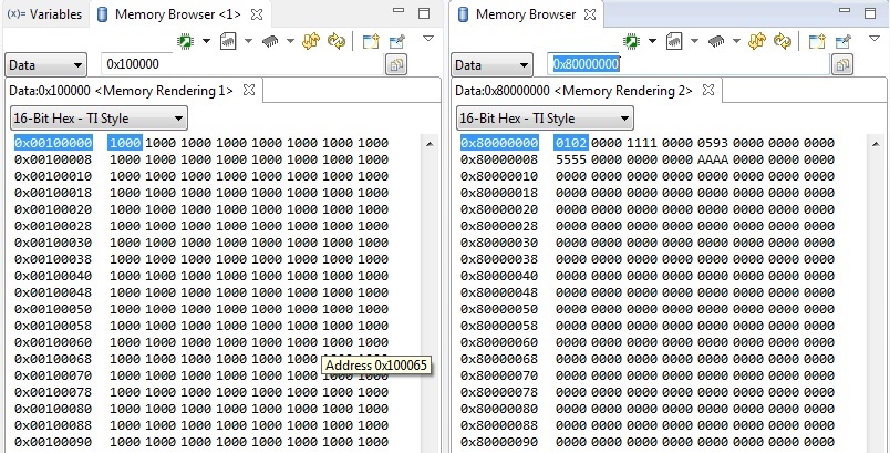
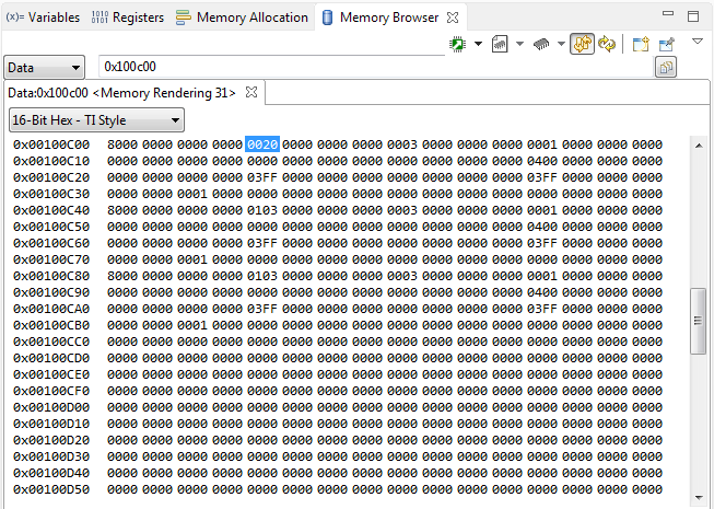
I still see that the data is 32bits in memory map.At address  0x8000 0000 while we used configuration for cs2 (address 0x10 0000)

we tried to change CSs between cs2 and cs0, also tried to disconnect cs0/2 from FPGA(cycloneIII) and still the data loads to 0x8000 0000.

"data" means registers in FPGA.

any suggestion what did we configure wrong ?

tnx.

  • Hi,

    CS0 is chip select for SDRAM interface (0x8000_0000) so that should not be used for ASYNC interface. CS2 is correct chip select for ASYNC interface.

    Are you seeing the correct data @0x10_0000 address? If yes then ignore the data seen @ address 0x8000_0000. Controller will latch the data which is on the bus so you'll see something even @ addres 0x8000_0000.

    Regards,

    Vivek Singh

  • Hi Vivik thank you for your reply.
    This is a problem, we don't see 0x10 0000 by cs2 , only 0x8000 0000 . 

    in 0x8000 0000 we see correct data value from FPGA, but can't update . 

    when we try write to data in space of cs2 (0x10 0000 ), all the data is changing to this value (data)

    Our system pins configure :


    in main() 

      setup_emif1_pinmux_async_16bit(0);
    
    
       // setup_emif1_pinmux_sdram_16bit(0);
    
       GPIO_SetupPinMux(99,0,0);	//	CFG_S2
    
       EALLOW;
       GpioCtrlRegs.GPDGMUX1.bit.GPIO99 = 0;
       GpioCtrlRegs.GPDDIR.bit.GPIO99 = 1;
       EDIS;
    
       GpioDataRegs.GPDDAT.bit.GPIO99 = 1;
    
    
    //   Emif1Initialize();   // for reset Emif1
    
    
    	// Configure to run EMIF1 on half Rate (EMIF1CLK = CPU1SYSCLK/2)
    	EALLOW;
    	ClkCfgRegs.PERCLKDIVSEL.bit.EMIF1CLKDIV = 0x1;
    	EDIS;
    
       EALLOW;
    	// Grab EMIF1 For CPU1
    	Emif1ConfigRegs.EMIF1MSEL.all = 0x93A5CE71;
    	if (Emif1ConfigRegs.EMIF1MSEL.all != 0x1)
    	{
    	  ErrCount++;
    	}
    
    	// Disable Access Protection (CPU_FETCH/CPU_WR/DMA_WR)
    	Emif1ConfigRegs.EMIF1ACCPROT0.all = 0x0;
    	if (Emif1ConfigRegs.EMIF1ACCPROT0.all != 0x0)
    	{
    	  ErrCount++;
    	}
    
    	// Commit the configuration related to protection. Till this bit remains set
    	// content of EMIF1ACCPROT0 register can't be changed.
    	Emif1ConfigRegs.EMIF1COMMIT.all = 0x1;
    	if(Emif1ConfigRegs.EMIF1COMMIT.all != 0x1)
    	{
    	 ErrCount++;
    	}
    
    	// Lock the configuration so that EMIF1COMMIT register can't be changed any more.
    	Emif1ConfigRegs.EMIF1LOCK.all = 0x1;
    	if (Emif1ConfigRegs.EMIF1LOCK.all != 1)
    	{
    	  ErrCount++;
    	}
    
    	EDIS;

    /////////////////////////////////////////////////////////////////////////////////////////////////////////////////////////////////////

    //function for EMIF1 GPIO pin setup
    void setup_emif1_pinmux_async_16bit(Uint16 cpu_sel)
    {
        Uint16 i;
    
        // data pins XD0-15
        for (i=69; i<=83;i++)
        {
       // 	if((i != 78)||(i != 77))
            GPIO_SetupPinMux(i,cpu_sel,2);
        }
    
        //address pins XA0-12
        for (i=38; i<=52;i++)
        {
        	if((i != 42)||(i != 43))
        		GPIO_SetupPinMux(i,cpu_sel,2);
        }
        //address pins XA13-19
        for (i=85; i<=92;i++)
        {
            GPIO_SetupPinMux(i,cpu_sel,2);
        }
    
        GPIO_SetupPinMux(31,cpu_sel,2);	//	EM1WEn
        GPIO_SetupPinMux(32,cpu_sel,2);	//	EM1CS0n
        GPIO_SetupPinMux(33,cpu_sel,2);	//	EM1R/nW
        GPIO_SetupPinMux(34,cpu_sel,2);	//	EM1CS2n
        GPIO_SetupPinMux(36,cpu_sel,2);	//	EM1WAIT
        GPIO_SetupPinMux(37,cpu_sel,2);	//	EM1OEn
        GPIO_SetupPinMux(30,cpu_sel,2);	//	EM1CLK
    
        GPIO_SetupPinMux(133,cpu_sel,0);	//	GPIO133
    
     }   


    Thank you for the answer.

    BR,

    Radion M.

  • Hi,

    You need to probe the output from FPGA to see if the data is getting driven correctly when CS2 toggle. Look like the CS signals are not connected correctly. On F28377D device side, CS0 has specific meaning. It's for SDRAM interface only where as on FPGA side CS0 could be just another ASYNC chip select. You may want to connect CS2 from device side to CS0 of FPGA and see if that helps.

    Regards,
    Vivek Singh
  • hi, Vivek

    In previous mail I've sent accidentally the picture of FPGA side.  

    this picture is side of  TI you can see here the pins config. : 

    When we past the part of  GPIOs configuration on DSP,  the memory at adress 0x8000 0000 is filled with FPGA's data regardless CS0/CS2 .


    GPIO_SetupPinMux(31,cpu_sel,2); // EM1WEn
    GPIO_SetupPinMux(32,cpu_sel,0); // EM1CS0n
    GPIO_SetupPinMux(33,cpu_sel,2); // EM1R/nW
    GPIO_SetupPinMux(34,cpu_sel,2); // EM1CS2n
    GPIO_SetupPinMux(36,cpu_sel,2); // EM1WAIT
    GPIO_SetupPinMux(37,cpu_sel,2); // EM1OEn
    GPIO_SetupPinMux(30,cpu_sel,2); // EM1CLK

    and i tried to configure CS0 as GPIO - input and not as CS, I still see the same memory browser(from prevision post).

    In prevision generation of DSP(28335) in the Emif protocol  was signal 'Ready', in current version we have 'Wait', what is the logic behind it?

     is it should work the opposite?

  • Hi,

    and i tried to configure CS0 as GPIO - input and not as CS, I still see the same memory browser(from prevision post).

    I do not know the logic programmed inside FPGA so can not comment on this. EMIF will capture the data put on the data-bus by FPGA. You need to scope the control signal and some data bus to check how data is changing on bus wrt control signals.

    In prevision generation of DSP(28335) in the Emif protocol  was signal 'Ready', in current version we have 'Wait', what is the logic behind it?

    Purpose of both the signal is same (just different name because it's different IP).

    Regards,

    Vivek Singh

  • hi,
    thank you for your reply,

    what may be the reason that we see FPGA's data on 0x8000 0000 and not at 0x10 0000? regardless CS, we checked with Scope the signals looks correct.
  • Could you send the snapshot of the scope for CS and other control signals?

    Regards,

    Vivek Singh
  • Closing the thread. If issue is not resolved then please re-open this thread and provide required info or open new E2E post.
  • hi Vivek ,

    I succeeded to  load through emif data from fpga , but the address incorrect (to walk around this problem I need to shift / multiply by 2 ) . for example if i want write to address 0x600 , i use:

    #define EXT_FPGA_OFFSET                        (Uint32)0x00000100000

    #define WR_EXT_FPGA(ADDR, DATA)         (*(Uint16 *)(EXT_FPGA_OFFSET|(ADDR)<<1) = (DATA))
    #define RD_EXT_FPGA(ADDR)                    (*(Uint16 *)(EXT_FPGA_OFFSET|(ADDR)<<1))

    WR_EXT_FPGA(0x602, DATA) i see in 0xC04

    -----------------------------------------------------------------------------------------------------------------------------------------------------------------

    NOTE:

    In tms320f28335 I have not encountered with that problem, I simply used without shifting and was able to receive the data in correct place.

    For example: 

    #define EXT_FPGA_OFFSET                        (Uint32)0x00000200000

    #define WR_EXT_FPGA(ADDR, DATA)         (*(Uint16 *)(EXT_FPGA_OFFSET|(ADDR)) = (DATA))
    #define RD_EXT_FPGA(ADDR)                    (*(Uint16 *)(EXT_FPGA_OFFSET|(ADDR))

    -----------------------------------------------------------------------------------------------------------------------------------------------------------------

    My questions are:

    1. How can I solve this without shift by 2? Maybe there is a way to config the emif module so the addresses will be like in SDRAM (there I have NM bit)?

    2.  I config system clock to 120Mhz

        InitSysPll(XTAL_OSC,IMULT_8,FMULT_1,PLLCLK_BY_4); //PLLSYSCLK = 30MHz(XTAL_OSC) * 8 (IMULT) * 1 (FMULT) / 2 (PLLCLK_BY_2)

        and want config Emif clock divided  from this SysClock to 30Mhz to works with FPGA (Emif have ClkCfgRegs.PERCLKDIVSEL.bit.EMIF1CLKDIV = 0x1;) this           option only divide by 2 the Sysclock (my clock now is 60Mhz instead 30 Mhz).

        Is there anything else that can effect the emif clock?

    BR,

    Rodion.

  • Hi Rodion,

    On this device the address lines (Ax) of EMIF module are for 32bit memory devices. If connecting 16bit memory device then A0 of memory should be connected to EMxBA1 pin of device (and not to A0). Please refer "Figure 25-9. EMIF to 8-bit/16-bit Memory Interface" of TRM for the same. Could you check that this is how address lines are connected on your board?

    Is there anything else that can effect the emif clock?

    We only have divide by 2 option for EMIF clock. If FPGA is slow then you should be able to change the ASYNC timing. Right?

    Regards,

    Vivek Singh