Other Parts Discussed in Thread: CONTROLSUITE
Hello everyone,
I am trying to run a program from flash but face some issues with that for which I need some help. In general: I generate PWM signals (ePWM1 and ePWM2) and do an ADC reading inside the adc_isr. Using RAM, the code works perfectly fine. To program in flash, I followed the SPRA958L reference and the example "Example_28335_Flash" from controlSuite very closely. What I did:
1. Remove the 28335_RAM_Ink.cmd from my project
2. Add the F28335.cmd into my project (Right click on my project -> Add files -> F28335)
3. Add the following piece of code into my main function:
	/*** Initialize the PIE_RAM ***/
	PieCtrlRegs.PIECTRL.bit.ENPIE = 0; // Disable the PIE
	asm(" EALLOW"); // Enable EALLOW protected register access
	memcpy(&PieVectTable, &PieVectTableInit, 256);
	asm(" EDIS"); // Disable EALLOW protected register access
4. Add the memcpy command into my code:
	// Copy time critical code and Flash setup code to RAM
	// This includes the following ISR functions: epwm1_timer_isr(), epwm2_timer_isr()
	// epwm3_timer_isr and and InitFlash();
	// The  RamfuncsLoadStart, RamfuncsLoadEnd, and RamfuncsRunStart
	// symbols are created by the linker. Refer to the F28335.cmd file.

	   memcpy(&RamfuncsRunStart, &RamfuncsLoadStart, (Uint32)&RamfuncsLoadSize);
5. Calling the InitFlash() function:
	   // Call Flash Initialization to setup flash waitstates
	   // This function must reside in RAM
	      InitFlash();
6. Activate the flash in my adc_isr:
// Activate flash
	   EALLOW;
	   FlashRegs.FPWR.bit.PWR = FLASH_ACTIVE;
	   FlashRegs.FSTATUS.bit.V3STAT = 1; // Clear the 3VSTAT bit
	   FlashRegs.FSTDBYWAIT.bit.STDBYWAIT = 0x01FF; // Sleep to standby cycles
	   FlashRegs.FACTIVEWAIT.bit.ACTIVEWAIT = 0x01FF; // Standby to active cycles
	   FlashRegs.FBANKWAIT.bit.RANDWAIT = 3; // F280x Random access wait states
	   FlashRegs.FBANKWAIT.bit.PAGEWAIT = 3; // F280x Paged access wait states
	   FlashRegs.FOTPWAIT.bit.OTPWAIT = 5; // F280x OTP wait states
	   FlashRegs.FOPT.bit.ENPIPE = 1; // Enable the flash pipeline
	   EDIS;
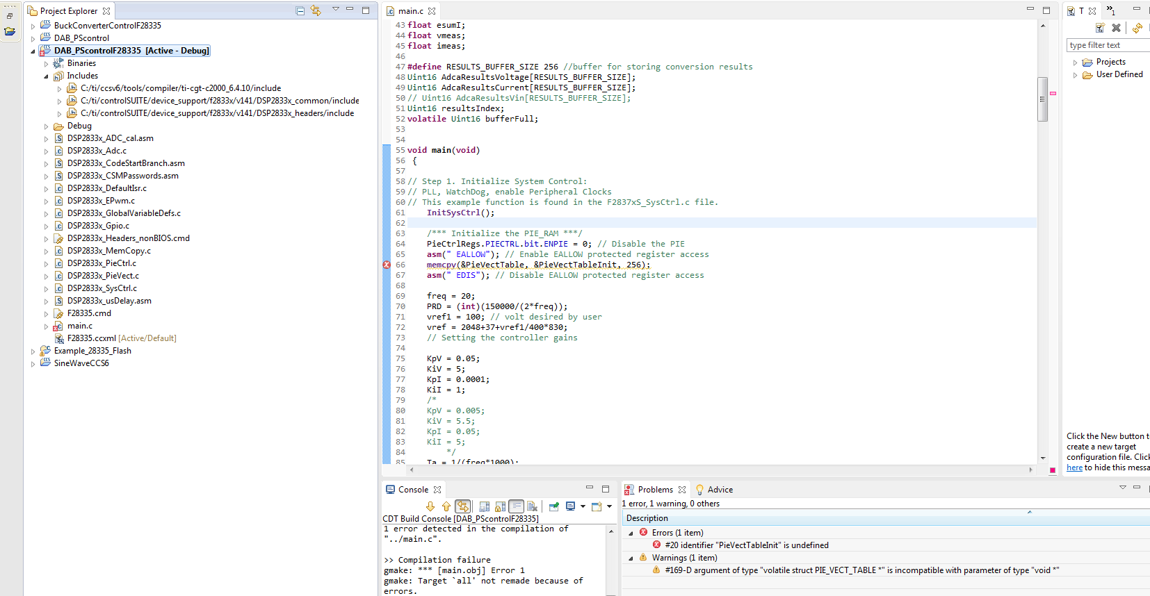
When I click the "Hammer tool" button in CCS, I get the error "#20 identifier PieVectTableInit is undefined". I guess I miss something that I cannot see. The complete code of my project:
#include "DSP28x_Project.h" // Device Headerfile and Examples Include File
#include <math.h>
#include <string.h>
// Prototype statements for functions found within this file.
void InitEPwm1(void);
void InitEPwm2(void);
void InitEPwm3(void);
void InitEPwm4(void);
void InitializeADC(void);
// Functions that will be run from RAM need to be assigned to
// a different section. This section will then be mapped using
// the linker cmd file.
#pragma CODE_SECTION(adc_isr, "ramfuncs");
__interrupt void adc_isr(void);
// These are defined by the linker (see F28335.cmd)
extern Uint16 RamfuncsLoadStart;
extern Uint16 RamfuncsLoadEnd;
extern Uint16 RamfuncsRunStart;
extern Uint16 RamfuncsLoadSize;
// User defined
int PRD;
float freq;
float ADCgain;
float vref;
float vref1;
float iref;
float errorvoltage;
float errorcurrent;
float dutycycle;
float saturation;
float KpV;
float KiV;
float KpI;
float KiI;
float Ta;
float esumV;
float esumI;
float vmeas;
float imeas;
#define RESULTS_BUFFER_SIZE 256 //buffer for storing conversion results
Uint16 AdcaResultsVoltage[RESULTS_BUFFER_SIZE];
Uint16 AdcaResultsCurrent[RESULTS_BUFFER_SIZE];
// Uint16 AdcaResultsVin[RESULTS_BUFFER_SIZE];
Uint16 resultsIndex;
volatile Uint16 bufferFull;
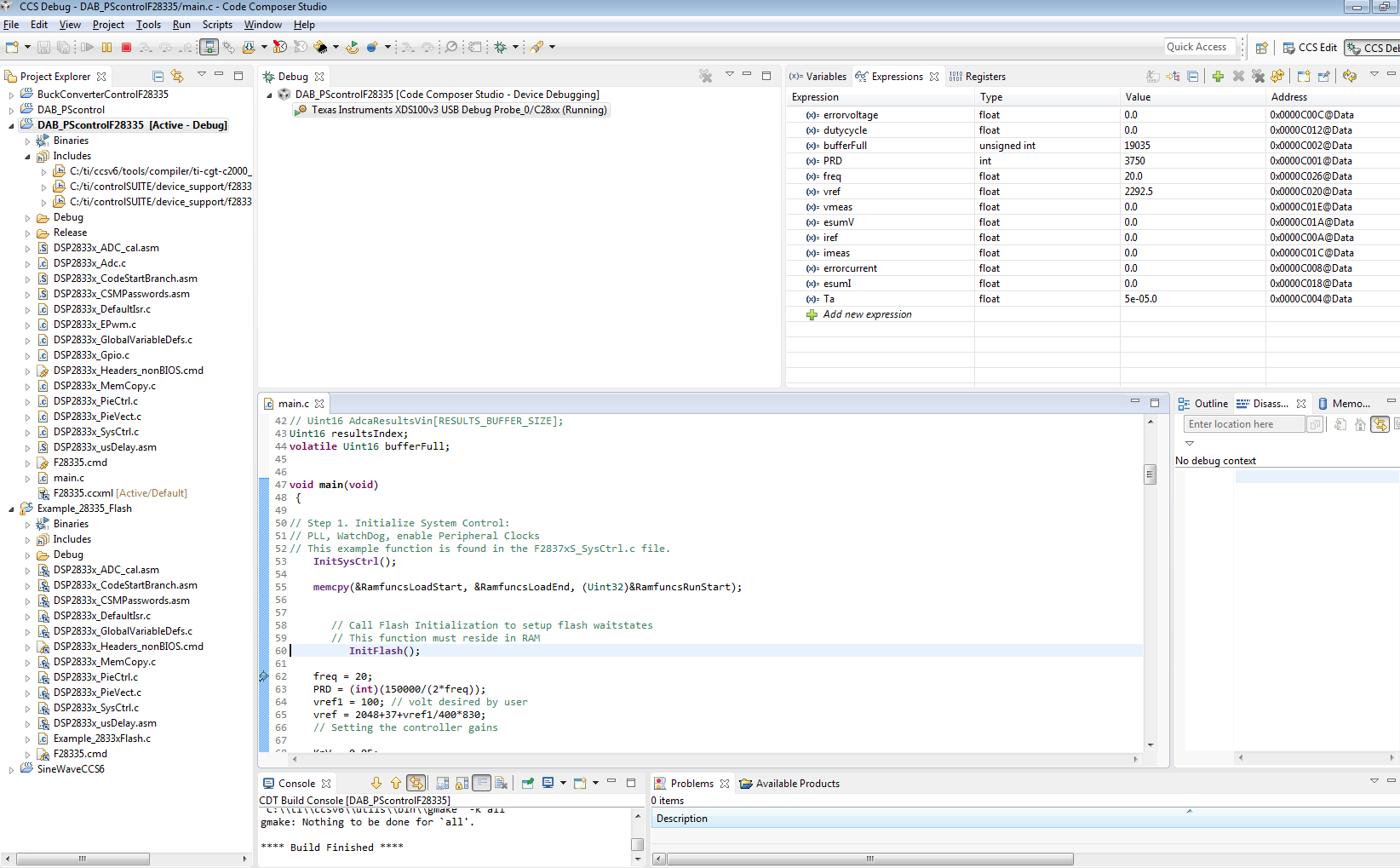
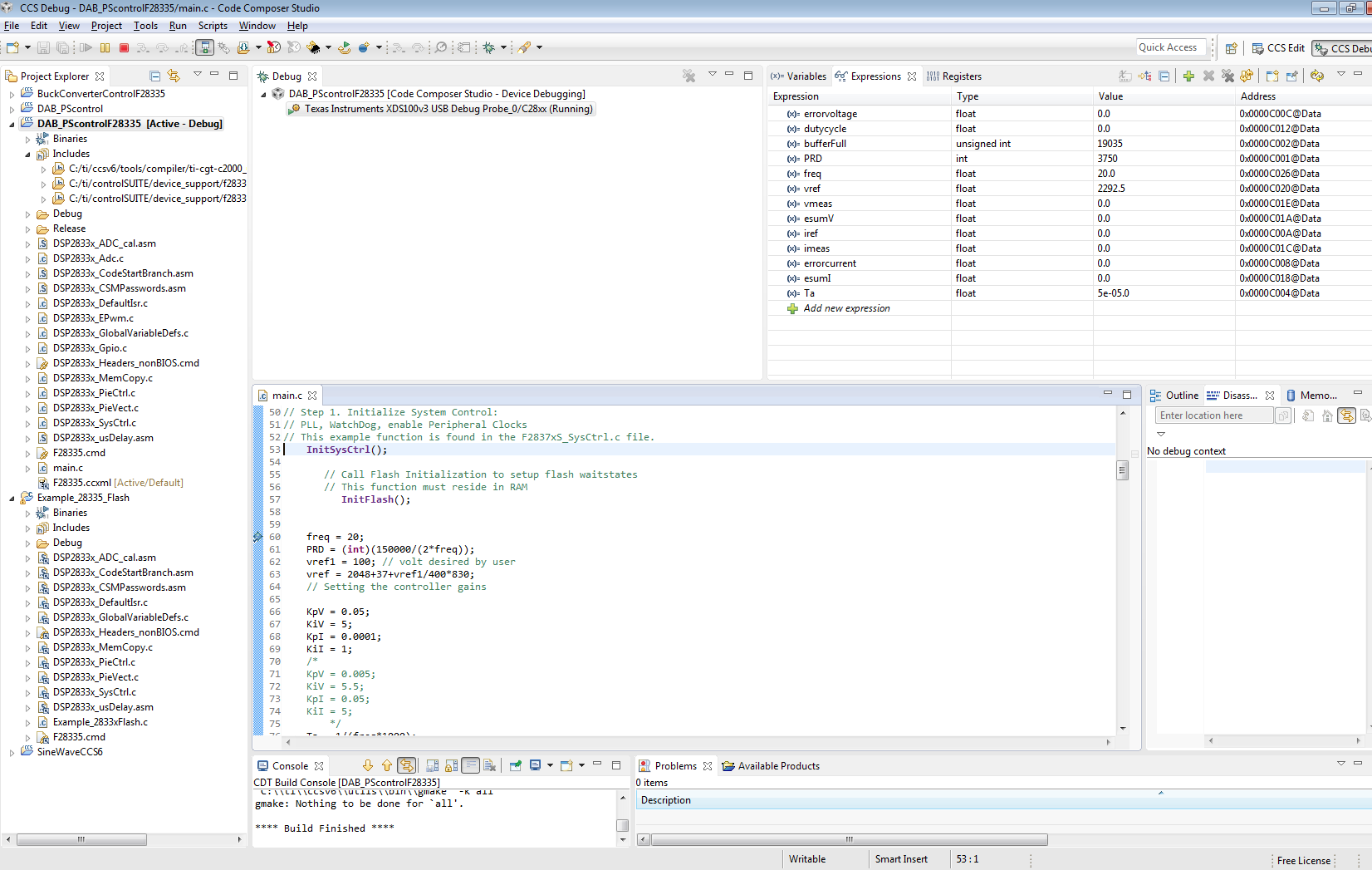
void main(void)
{
// Step 1. Initialize System Control:
// PLL, WatchDog, enable Peripheral Clocks
// This example function is found in the F2837xS_SysCtrl.c file.
InitSysCtrl();
/*** Initialize the PIE_RAM ***/
PieCtrlRegs.PIECTRL.bit.ENPIE = 0; // Disable the PIE
asm(" EALLOW"); // Enable EALLOW protected register access
memcpy(&PieVectTable, &PieVectTableInit, 256);
asm(" EDIS"); // Disable EALLOW protected register access
freq = 20;
PRD = (int)(150000/(2*freq));
vref1 = 100; // volt desired by user
vref = 2048+37+vref1/400*830;
// Setting the controller gains
KpV = 0.05;
KiV = 5;
KpI = 0.0001;
KiI = 1;
/*
KpV = 0.005;
KiV = 5.5;
KpI = 0.05;
KiI = 5;
*/
Ta = 1/(freq*1000);
esumV = 0;
esumI = 0;
errorvoltage = 0;
errorcurrent = 0;
dutycycle = 0;
vmeas = 0;
imeas = 0;
iref = 0;
// Define ADCCLK clock frequency ( less than or equal to 25 MHz )
// Assuming InitSysCtrl() has set SYSCLKOUT to 150 MHz
EALLOW;
SysCtrlRegs.HISPCP.all = 3;
EDIS;
// Step 2. Initialize GPIO:
// This example function is found in the F2837xS_Gpio.c file and
// illustrates how to set the GPIO to its default state.
InitGpio();
// For this case just init GPIO pins for ePWM1, ePWM2, ePWM3
// These functions are in the F2837xS_EPwm.c file
InitEPwm1Gpio();
InitEPwm2Gpio();
InitEPwm3Gpio();
InitEPwm4Gpio();
InitAdc(); // For this example, init the ADC
// Step 3. Clear all interrupts and initialize PIE vector table:
// Disable CPU interrupts
DINT;
// Initialize the PIE control registers to their default state.
// The default state is all PIE interrupts disabled and flags
// are cleared.
// This function is found in the F2837xS_PieCtrl.c file.
InitPieCtrl();
// Disable CPU interrupts and clear all CPU interrupt flags:
IER = 0x0000;
IFR = 0x0000;
// Initialize the PIE vector table with pointers to the shell Interrupt
// Service Routines (ISR).
// This will populate the entire table, even if the interrupt
// is not used in this example. This is useful for debug purposes.
// The shell ISR routines are found in F2837xS_DefaultIsr.c.
// This function is found in F2837xS_PieVect.c.
InitPieVectTable();
// Interrupts that are used in this example are re-mapped to
// ISR functions found within this file.
EALLOW; // This is needed to write to EALLOW protected registers
PieVectTable.ADCINT = &adc_isr;
EDIS; // This is needed to disable write to EALLOW protected registers
// Step 4. Initialize the Device Peripherals:
// For this example, only initialize the ePWM and ADC
EALLOW;
SysCtrlRegs.PCLKCR0.bit.TBCLKSYNC = 0;
EDIS;
InitEPwm1();
InitEPwm2();
InitEPwm3();
InitEPwm4();
InitializeADC();
//Initialize results buffer
for(resultsIndex = 0; resultsIndex < RESULTS_BUFFER_SIZE; resultsIndex++)
{
AdcaResultsVoltage[resultsIndex] = 0;
AdcaResultsCurrent[resultsIndex] = 0;
// AdcaResultsVin[resultsIndex] = 0;
}
resultsIndex = 0;
bufferFull = 0;
EALLOW;
SysCtrlRegs.PCLKCR0.bit.TBCLKSYNC =1;
EDIS;
// Copy time critical code and Flash setup code to RAM
// This includes the following ISR functions: epwm1_timer_isr(), epwm2_timer_isr()
// epwm3_timer_isr and and InitFlash();
// The RamfuncsLoadStart, RamfuncsLoadEnd, and RamfuncsRunStart
// symbols are created by the linker. Refer to the F28335.cmd file.
memcpy(&RamfuncsRunStart, &RamfuncsLoadStart, (Uint32)&RamfuncsLoadSize);
// Call Flash Initialization to setup flash waitstates
// This function must reside in RAM
InitFlash();
// Enable ADCINT in PIE
PieCtrlRegs.PIEIER1.bit.INTx6 = 1;
IER |= M_INT1; // Enable CPU Interrupt 1
EINT; // Enable Global interrupt INTM
ERTM; // Enable Global realtime interrupt DBGM
// Step 6. IDLE loop. Just sit and loop forever (optional):
//take conversions indefinitely in loop
do
{
//wait while ePWM causes ADC conversions, which then cause interrupts,
//which fill the results buffer, eventually setting the bufferFull
//flag
while(!bufferFull);
bufferFull = 0; //clear the buffer full flag
}while(1);
}
/* Interrupt service routine reading the output voltage and generating the PWM */
__interrupt void adc_isr(void)
{
// Activate flash
EALLOW;
FlashRegs.FPWR.bit.PWR = FLASH_ACTIVE;
FlashRegs.FSTATUS.bit.V3STAT = 1; // Clear the 3VSTAT bit
FlashRegs.FSTDBYWAIT.bit.STDBYWAIT = 0x01FF; // Sleep to standby cycles
FlashRegs.FACTIVEWAIT.bit.ACTIVEWAIT = 0x01FF; // Standby to active cycles
FlashRegs.FBANKWAIT.bit.RANDWAIT = 3; // F280x Random access wait states
FlashRegs.FBANKWAIT.bit.PAGEWAIT = 3; // F280x Paged access wait states
FlashRegs.FOTPWAIT.bit.OTPWAIT = 5; // F280x OTP wait states
FlashRegs.FOPT.bit.ENPIPE = 1; // Enable the flash pipeline
EDIS;
resultsIndex++;
/* Do the ADC reading for voltage and current */
AdcaResultsVoltage[resultsIndex] = AdcRegs.ADCRESULT0 >>4; // Voltage Vout
AdcaResultsCurrent[resultsIndex] = AdcRegs.ADCRESULT1 >>4; // Current IL
// AdcaResultsVin[resultsIndex] = AdcRegs.ADCRESULT2 >>4; // Voltage Vin
if(RESULTS_BUFFER_SIZE <= resultsIndex)
{
resultsIndex = 0;
bufferFull = 1;
}
// Reinitialize for next ADC sequence
AdcRegs.ADCTRL2.bit.RST_SEQ1 = 1; // Reset SEQ1
AdcRegs.ADCST.bit.INT_SEQ1_CLR = 1; // Clear INT SEQ1 bit
PieCtrlRegs.PIEACK.all = PIEACK_GROUP1; // Acknowledge interrupt to PIEg
}
void InitEPwm1()
{
EPwm1Regs.TBPRD = PRD; // Set timer period
EPwm1Regs.TBPHS.half.TBPHS = 0x0000; // Phase is 0
EPwm1Regs.TBCTR = 0x0000; // Clear counter
// Setup TBCLK
EPwm1Regs.ETSEL.bit.SOCAEN = 10; //enable SOCA
EPwm1Regs.ETSEL.bit.SOCASEL = 4; // Select SOC on up-count
EPwm1Regs.ETPS.bit.SOCAPRD = 1; // Generate pulse on 1st event
EPwm1Regs.TBCTL.bit.CTRMODE = TB_COUNT_UPDOWN; // Count up
EPwm1Regs.TBCTL.bit.PHSEN = TB_ENABLE; // Disable phase loading
EPwm1Regs.TBCTL.bit.PRDLD = TB_SHADOW;
EPwm1Regs.TBCTL.bit.SYNCOSEL = TB_CTR_ZERO;
EPwm1Regs.CMPCTL.bit.SHDWAMODE = CC_SHADOW;
EPwm1Regs.CMPCTL.bit.SHDWBMODE = CC_SHADOW;
EPwm1Regs.CMPCTL.bit.LOADAMODE = CC_CTR_ZERO;
EPwm1Regs.CMPCTL.bit.LOADBMODE = CC_CTR_ZERO;
EPwm1Regs.TBCTL.bit.HSPCLKDIV = TB_DIV1; // Clock ratio to SYSCLKOUT
EPwm1Regs.TBCTL.bit.CLKDIV = TB_DIV1; // Slow just to observe on the
// scope
EPwm1Regs.CMPA.half.CMPA=0.5*PRD;
// Set actions
EPwm1Regs.AQCTLA.bit.CAU = AQ_CLEAR; // Set PWM2A on Zero
EPwm1Regs.AQCTLA.bit.CAD = AQ_SET;
EPwm1Regs.AQCTLB.bit.CAU = AQ_SET; // Set PWM2A on Zero
EPwm1Regs.AQCTLB.bit.CAD = AQ_CLEAR;
// Setup Deadband
EPwm1Regs.DBCTL.bit.OUT_MODE = DB_FULL_ENABLE;
EPwm1Regs.DBCTL.bit.POLSEL = DB_ACTV_HIC;
EPwm1Regs.DBCTL.bit.IN_MODE = DBA_ALL;
EPwm1Regs.DBRED = 0.05*150;
EPwm1Regs.DBFED = 0.05*150;
}
void InitEPwm2()
{
EPwm2Regs.TBPRD = PRD; // Set timer period
EPwm2Regs.TBPHS.half.TBPHS = 165; // Phase is 0
EPwm2Regs.TBCTR = 0x0000; // Clear counter
// Setup TBCLK
EPwm2Regs.TBCTL.bit.CTRMODE = TB_COUNT_UPDOWN; // Count up
EPwm2Regs.TBCTL.bit.PHSEN = TB_ENABLE; // Disable phase loading
EPwm2Regs.TBCTL.bit.PRDLD = TB_SHADOW;
EPwm2Regs.TBCTL.bit.SYNCOSEL = TB_SYNC_IN;
EPwm2Regs.CMPCTL.bit.SHDWAMODE = CC_SHADOW;
EPwm2Regs.CMPCTL.bit.SHDWBMODE = CC_SHADOW;
EPwm2Regs.CMPCTL.bit.LOADAMODE = CC_CTR_ZERO;
EPwm2Regs.CMPCTL.bit.LOADBMODE = CC_CTR_ZERO;
EPwm2Regs.TBCTL.bit.HSPCLKDIV = TB_DIV1; // Clock ratio to SYSCLKOUT
EPwm2Regs.TBCTL.bit.CLKDIV = TB_DIV1; // Slow just to observe on the
// scope
EPwm2Regs.CMPA.half.CMPA=0.5*PRD;
// Set actions
EPwm2Regs.AQCTLA.bit.CAU = AQ_CLEAR; // Set PWM2A on Zero
EPwm2Regs.AQCTLA.bit.CAD = AQ_SET;
EPwm2Regs.AQCTLB.bit.CAU = AQ_SET; // Set PWM2A on Zero
EPwm2Regs.AQCTLB.bit.CAD = AQ_CLEAR;
// Setup Deadband
EPwm2Regs.DBCTL.bit.OUT_MODE = DB_FULL_ENABLE;
EPwm2Regs.DBCTL.bit.POLSEL = DB_ACTV_HIC;
EPwm2Regs.DBCTL.bit.IN_MODE = DBA_ALL;
EPwm2Regs.DBRED = 0.05*150;
EPwm2Regs.DBFED = 0.05*150;
}
void InitEPwm3()
{
EPwm3Regs.TBPRD = PRD; // Set timer period
EPwm3Regs.TBPHS.half.TBPHS = 0x0000; // Phase is 0
EPwm3Regs.TBCTR = 0x0000; // Clear counter
// Setup TBCLK
EPwm3Regs.TBCTL.bit.CTRMODE = TB_COUNT_UPDOWN; // Count up
EPwm3Regs.TBCTL.bit.PHSEN = TB_ENABLE; // Disable phase loading
EPwm3Regs.TBCTL.bit.PRDLD = TB_SHADOW;
EPwm3Regs.TBCTL.bit.SYNCOSEL = TB_SYNC_IN;
EPwm3Regs.CMPCTL.bit.SHDWAMODE = CC_SHADOW;
EPwm3Regs.CMPCTL.bit.SHDWBMODE = CC_SHADOW;
EPwm3Regs.CMPCTL.bit.LOADAMODE = CC_CTR_ZERO;
EPwm3Regs.CMPCTL.bit.LOADBMODE = CC_CTR_ZERO;
EPwm3Regs.TBCTL.bit.HSPCLKDIV = TB_DIV1; // Clock ratio to SYSCLKOUT
EPwm3Regs.TBCTL.bit.CLKDIV = TB_DIV1; // Slow just to observe on the
// scope
EPwm3Regs.CMPA.half.CMPA=0.5*PRD;
// Set actions
EPwm3Regs.AQCTLA.bit.CAU = AQ_CLEAR; // Set PWM2A on Zero
EPwm3Regs.AQCTLA.bit.CAD = AQ_SET;
EPwm3Regs.AQCTLB.bit.CAU = AQ_SET; // Set PWM2A on Zero
EPwm3Regs.AQCTLB.bit.CAD = AQ_CLEAR;
// Setup Deadband
EPwm3Regs.DBCTL.bit.OUT_MODE = DB_DISABLE;
EPwm3Regs.DBCTL.bit.POLSEL = DB_ACTV_HIC;
EPwm3Regs.DBCTL.bit.IN_MODE = DBA_ALL;
EPwm3Regs.DBRED = 0.2*150;
EPwm3Regs.DBFED = 0.2*150;
}
void InitEPwm4()
{
EPwm4Regs.TBPRD = PRD; // Set timer period
EPwm4Regs.TBPHS.half.TBPHS = 0.3*100; // Phase is 0
EPwm4Regs.TBCTR = 0x0000; // Clear counter
// Setup TBCLK
EPwm4Regs.TBCTL.bit.CTRMODE = TB_COUNT_UPDOWN; // Count up
EPwm4Regs.TBCTL.bit.PHSEN = TB_ENABLE; // Disable phase loading
EPwm4Regs.TBCTL.bit.PRDLD = TB_SHADOW;
EPwm4Regs.TBCTL.bit.SYNCOSEL = TB_SYNC_IN;
EPwm4Regs.CMPCTL.bit.SHDWAMODE = CC_SHADOW;
EPwm4Regs.CMPCTL.bit.SHDWBMODE = CC_SHADOW;
EPwm4Regs.CMPCTL.bit.LOADAMODE = CC_CTR_ZERO;
EPwm4Regs.CMPCTL.bit.LOADBMODE = CC_CTR_ZERO;
EPwm4Regs.TBCTL.bit.HSPCLKDIV = TB_DIV1; // Clock ratio to SYSCLKOUT
EPwm4Regs.TBCTL.bit.CLKDIV = TB_DIV1; // Slow just to observe on the
// scope
EPwm4Regs.CMPA.half.CMPA=0.5*PRD;
// Set actions
EPwm4Regs.AQCTLA.bit.CAU = AQ_CLEAR; // Set PWM2A on Zero
EPwm4Regs.AQCTLA.bit.CAD = AQ_SET;
EPwm4Regs.AQCTLB.bit.CAU = AQ_SET; // Set PWM2A on Zero
EPwm4Regs.AQCTLB.bit.CAD = AQ_CLEAR;
// Setup Deadband
EPwm4Regs.DBCTL.bit.OUT_MODE = DB_DISABLE;
EPwm4Regs.DBCTL.bit.POLSEL = DB_ACTV_HIC;
EPwm4Regs.DBCTL.bit.IN_MODE = DBA_ALL;
EPwm4Regs.DBRED = 0.2*150;
EPwm4Regs.DBFED = 0.2*150;
}
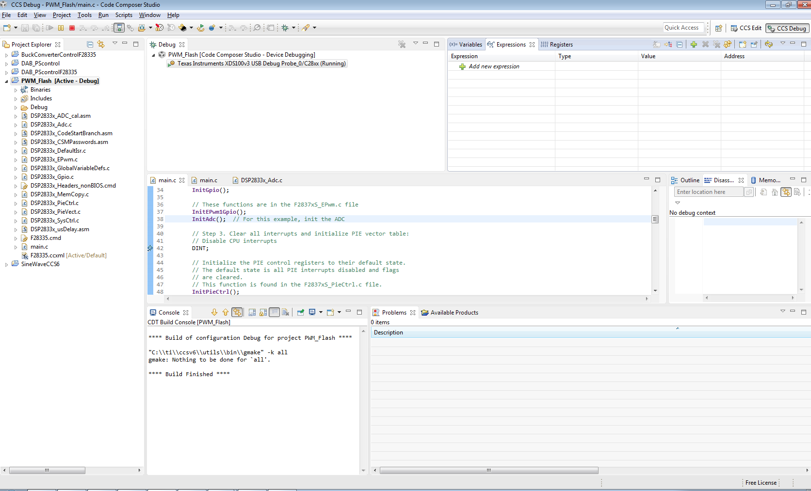
void InitializeADC()
{
// Configure ADC
AdcRegs.ADCMAXCONV.all = 0x0002; // Setup 2 conv's on SEQ1
AdcRegs.ADCCHSELSEQ1.bit.CONV00 = 0x0; // Setup ADCINA0 as 1st SEQ1 conv.
AdcRegs.ADCCHSELSEQ1.bit.CONV01 = 0x1; // Setup ADCINA1 as 2nd SEQ1 conv.
// AdcRegs.ADCCHSELSEQ1.bit.CONV02 = 0x2; // Setup ADCINA2 as 3rd SEQ1 conv.
AdcRegs.ADCTRL2.bit.EPWM_SOCA_SEQ1 = 1;// Enable SOCA from ePWM to start SEQ1
AdcRegs.ADCTRL2.bit.INT_ENA_SEQ1 = 1; // Enable SEQ1 interrupt (every EOS)
}
The linker command file that I use:
/*
//###########################################################################
//
// FILE:	F28335.cmd
//
// TITLE:	Linker Command File For F28335 Device
//
//###########################################################################
// $TI Release: F2833x/F2823x Header Files and Peripheral Examples V141 $
// $Release Date: November  6, 2015 $
// $Copyright: Copyright (C) 2007-2015 Texas Instruments Incorporated -
//             http://www.ti.com/ ALL RIGHTS RESERVED $
//###########################################################################
*/

/* ======================================================
// For Code Composer Studio V2.2 and later
// ---------------------------------------
// In addition to this memory linker command file,
// add the header linker command file directly to the project.
// The header linker command file is required to link the
// peripheral structures to the proper locations within
// the memory map.
//
// The header linker files are found in <base>\DSP2833x_Headers\cmd
//
// For BIOS applications add:      DSP2833x_Headers_BIOS.cmd
// For nonBIOS applications add:   DSP2833x_Headers_nonBIOS.cmd
========================================================= */

/* ======================================================
// For Code Composer Studio prior to V2.2
// --------------------------------------
// 1) Use one of the following -l statements to include the
// header linker command file in the project. The header linker
// file is required to link the peripheral structures to the proper
// locations within the memory map                                    */

/* Uncomment this line to include file only for non-BIOS applications */
/* -l DSP2833x_Headers_nonBIOS.cmd */

/* Uncomment this line to include file only for BIOS applications */
/* -l DSP2833x_Headers_BIOS.cmd */

/* 2) In your project add the path to <base>\DSP2833x_headers\cmd to the
   library search path under project->build options, linker tab,
   library search path (-i).
/*========================================================= */

/* Define the memory block start/length for the F28335
   PAGE 0 will be used to organize program sections
   PAGE 1 will be used to organize data sections

    Notes:
          Memory blocks on F28335 are uniform (ie same
          physical memory) in both PAGE 0 and PAGE 1.
          That is the same memory region should not be
          defined for both PAGE 0 and PAGE 1.
          Doing so will result in corruption of program
          and/or data.

          L0/L1/L2 and L3 memory blocks are mirrored - that is
          they can be accessed in high memory or low memory.
          For simplicity only one instance is used in this
          linker file.

          Contiguous SARAM memory blocks can be combined
          if required to create a larger memory block.
 */


MEMORY
{
PAGE 0:    /* Program Memory */
           /* Memory (RAM/FLASH/OTP) blocks can be moved to PAGE1 for data allocation */

   ZONE0       : origin = 0x004000, length = 0x001000     /* XINTF zone 0 */
   RAML0       : origin = 0x008000, length = 0x001000     /* on-chip RAM block L0 */
   RAML1       : origin = 0x009000, length = 0x001000     /* on-chip RAM block L1 */
   RAML2       : origin = 0x00A000, length = 0x001000     /* on-chip RAM block L2 */
   RAML3       : origin = 0x00B000, length = 0x001000     /* on-chip RAM block L3 */
   ZONE6       : origin = 0x0100000, length = 0x100000    /* XINTF zone 6 */
   ZONE7A      : origin = 0x0200000, length = 0x00FC00    /* XINTF zone 7 - program space */
   FLASHH      : origin = 0x300000, length = 0x008000     /* on-chip FLASH */
   FLASHG      : origin = 0x308000, length = 0x008000     /* on-chip FLASH */
   FLASHF      : origin = 0x310000, length = 0x008000     /* on-chip FLASH */
   FLASHE      : origin = 0x318000, length = 0x008000     /* on-chip FLASH */
   FLASHD      : origin = 0x320000, length = 0x008000     /* on-chip FLASH */
   FLASHC      : origin = 0x328000, length = 0x008000     /* on-chip FLASH */
   FLASHA      : origin = 0x338000, length = 0x007F80     /* on-chip FLASH */
   CSM_RSVD    : origin = 0x33FF80, length = 0x000076     /* Part of FLASHA.  Program with all 0x0000 when CSM is in use. */
   BEGIN       : origin = 0x33FFF6, length = 0x000002     /* Part of FLASHA.  Used for "boot to Flash" bootloader mode. */
   CSM_PWL     : origin = 0x33FFF8, length = 0x000008     /* Part of FLASHA.  CSM password locations in FLASHA */
   OTP         : origin = 0x380400, length = 0x000400     /* on-chip OTP */
   ADC_CAL     : origin = 0x380080, length = 0x000009     /* ADC_cal function in Reserved memory */

   IQTABLES    : origin = 0x3FE000, length = 0x000b50     /* IQ Math Tables in Boot ROM */
   IQTABLES2   : origin = 0x3FEB50, length = 0x00008c     /* IQ Math Tables in Boot ROM */
   FPUTABLES   : origin = 0x3FEBDC, length = 0x0006A0     /* FPU Tables in Boot ROM */
   ROM         : origin = 0x3FF27C, length = 0x000D44     /* Boot ROM */
   RESET       : origin = 0x3FFFC0, length = 0x000002     /* part of boot ROM  */
   VECTORS     : origin = 0x3FFFC2, length = 0x00003E     /* part of boot ROM  */

PAGE 1 :   /* Data Memory */
           /* Memory (RAM/FLASH/OTP) blocks can be moved to PAGE0 for program allocation */
           /* Registers remain on PAGE1                                                  */

   BOOT_RSVD   : origin = 0x000000, length = 0x000050     /* Part of M0, BOOT rom will use this for stack */
   RAMM0       : origin = 0x000050, length = 0x0003B0     /* on-chip RAM block M0 */
   RAMM1       : origin = 0x000400, length = 0x000400     /* on-chip RAM block M1 */
   RAML4       : origin = 0x00C000, length = 0x001000     /* on-chip RAM block L1 */
   RAML5       : origin = 0x00D000, length = 0x001000     /* on-chip RAM block L1 */
   RAML6       : origin = 0x00E000, length = 0x001000     /* on-chip RAM block L1 */
   RAML7       : origin = 0x00F000, length = 0x001000     /* on-chip RAM block L1 */
   ZONE7B      : origin = 0x20FC00, length = 0x000400     /* XINTF zone 7 - data space */
   FLASHB      : origin = 0x330000, length = 0x008000     /* on-chip FLASH */
}

/* Allocate sections to memory blocks.
   Note:
         codestart user defined section in DSP28_CodeStartBranch.asm used to redirect code
                   execution when booting to flash
         ramfuncs  user defined section to store functions that will be copied from Flash into RAM
*/

SECTIONS
{

   /* Allocate program areas: */
   .cinit              : > FLASHA      PAGE = 0
   .pinit              : > FLASHA,     PAGE = 0
   .text               : > FLASHA      PAGE = 0
   codestart           : > BEGIN       PAGE = 0
   ramfuncs            : LOAD = FLASHD,
                         RUN = RAML0,
                         LOAD_START(_RamfuncsLoadStart),
                         LOAD_END(_RamfuncsLoadEnd),
                         RUN_START(_RamfuncsRunStart),
                         LOAD_SIZE(_RamfuncsLoadSize),
                         PAGE = 0

   csmpasswds          : > CSM_PWL     PAGE = 0
   csm_rsvd            : > CSM_RSVD    PAGE = 0

   /* Allocate uninitalized data sections: */
   .stack              : > RAMM1       PAGE = 1
   .ebss               : > RAML4       PAGE = 1
   .esysmem            : > RAMM1       PAGE = 1

   /* Initalized sections go in Flash */
   /* For SDFlash to program these, they must be allocated to page 0 */
   .econst             : > FLASHA      PAGE = 0
   .switch             : > FLASHA      PAGE = 0

   /* Allocate IQ math areas: */
   IQmath              : > FLASHC      PAGE = 0                  /* Math Code */
   IQmathTables     : > IQTABLES,  PAGE = 0, TYPE = NOLOAD

   /* Uncomment the section below if calling the IQNexp() or IQexp()
      functions from the IQMath.lib library in order to utilize the
      relevant IQ Math table in Boot ROM (This saves space and Boot ROM
      is 1 wait-state). If this section is not uncommented, IQmathTables2
      will be loaded into other memory (SARAM, Flash, etc.) and will take
      up space, but 0 wait-state is possible.
   */
   /*
   IQmathTables2    : > IQTABLES2, PAGE = 0, TYPE = NOLOAD
   {

              IQmath.lib<IQNexpTable.obj> (IQmathTablesRam)

   }
   */

   FPUmathTables    : > FPUTABLES, PAGE = 0, TYPE = NOLOAD

   /* Allocate DMA-accessible RAM sections: */
   DMARAML4         : > RAML4,     PAGE = 1
   DMARAML5         : > RAML5,     PAGE = 1
   DMARAML6         : > RAML6,     PAGE = 1
   DMARAML7         : > RAML7,     PAGE = 1

   /* Allocate 0x400 of XINTF Zone 7 to storing data */
   ZONE7DATA        : > ZONE7B,    PAGE = 1

   /* .reset is a standard section used by the compiler.  It contains the */
   /* the address of the start of _c_int00 for C Code.   /*
   /* When using the boot ROM this section and the CPU vector */
   /* table is not needed.  Thus the default type is set here to  */
   /* DSECT  */
   .reset              : > RESET,      PAGE = 0, TYPE = DSECT
   vectors             : > VECTORS     PAGE = 0, TYPE = DSECT

   /* Allocate ADC_cal function (pre-programmed by factory into TI reserved memory) */
   .adc_cal     : load = ADC_CAL,   PAGE = 0, TYPE = NOLOAD

}

/*
//===========================================================================
// End of file.
//===========================================================================
*/
A screenshot after compiling:
Any help is highly appreciated. Thank you.