This thread has been locked.

If you have a related question, please click the "Ask a related question" button in the top right corner. The newly created question will be automatically linked to this question.

ADC VREFHI settings for F28377 with ref3030

Other Parts Discussed in Thread: LMP7709, OPA320, OPA350, TMDSCNCD28379D, CONTROLSUITE

Hi,

  I am designing the schematic for F28377D and taking the F28377 ControlCard as reference.

  In the F28377 ControlCard the ADC module uses two ref3030 and a 4ch rail-to-rail input and output precision amplifier LMP7709 as voltage followers to set the reference-high.

  But I think the accuracy and output current is high enough for the ADC module and I consider that I do not need the voltage followers to achieve the impendance matching.

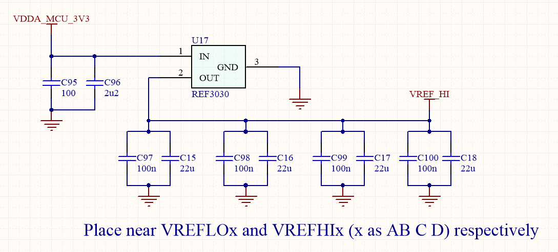
  So the ADC reference-high setting can be done as below. A 22uF capacitor for the 16-bit mode.

  Is there something wrong with my design? Are these voltage followers necessary?

  Looking forward to your reply.

  best regards,

  Di

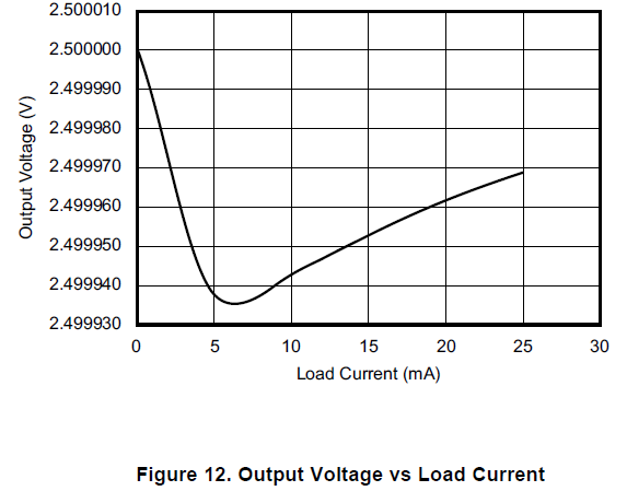
  • here is the figure of Output Voltage vs Load Current for REF3030.

    But I want to know the equal impedance of the ADC REFHI port. Where can I get the data?

  • Hi Di,


    The voltage followers are indeed necessary.  The VREFHI pins do not have a large static current draw (a little less than 200uA) but the dynamic currents are very large/sharp.  Driving the ADC inputs directly with the reference IC will result in reduced linearity performance in 16-bit mode and reduced dynamic performance in both 12-bit and 16-bit mode.  See this thread https://e2e.ti.com/support/microcontrollers/c2000/f/171/t/477506.

    I would also caution you that the initial ControlCard  erroneously used LMP7709 in a voltage follower configuration.  This is a decompensated amplifier, so it may become unstable in this configuration.  I would recommend both OPA320 and OPA350 as good choices for the reference driver for F2837x devices, as we have characterized the performance with these used as buffers.

  • One more point: You can get the schematics for the latest ControlCard revision in ControlSUITE in \controlSUITE\development_kits\~controlCARDs\TMDSCNCD28379D_v1_0\R1_3\. The reference circuit on this version utilizes OPA350.
  • Hi Devin,
    Thanks for your nice reply.
    I want to know why 0PA350 is a better choice in principle. As a voltage follower which parameters should be considered?
    Looking forward for your reply.
    Di
  • Hi Devin,

    looking at the schematics on sheet 4 there is a remark:

    SW2 and SW3 allow a user to choose between using a clean external reference (such that the full-scale of the ADC is 0 to Vref, where Vref must always be less than VDDA) or use VDDA as a reference (with reduced accuracy/precision).

    Does that mean, that if you want the Vref to be 3.3 V you can only use direct connection to VDDA.

    Or do you prefer 3.0 V reference in order to simplify the design? If you want to use 3.3 V reference, you would have to supply the buffers with 5 V even if they are rail to rail in order to keep stable 3.3 V reference output. This would probably mean to filter the 5 V supply line for analog use and it complicates the design and layout.

    From the device datasheet one can not find any reason no to use 3.3 V reference.

    Can you shine some light on this.

    Best regards, Mitja

  • Hi Mitja,

    The main reason to use the OPA350 vs the reference IC directly is that the op-amp has much higher drive bandwidth. The ADC reference needs to settle to much better than 1 LSB in one ADC clock cycle. Both the op-amp and the capacitor help with this, and you could theoretically get away with using a lower bandwidth driver if you use a very larger capacitor (but the capacitors needed are already pretty large).

    There is a hard requirement in the datasheet that VREFHI <= VDDA at all times. If you want to supply VREFHI as 3.3V from a non-VDDA source, then you need to set the nominal voltage for VDDA to be higher than normal and ensure that it never gets down as low as VREFHI. This is possible, but you end up with some difficult power supply design constraints and difficult power sequencing issues.