


Other Parts Discussed in Thread: TMS320F28335, BQ32000
Hello Everyone!
I need help in I2C communication of TMS320F28335 with real time clock(RTC) BQ32000
http://www.ti.com/lit/ds/symlink/bq32000.pdf
When I load my program I see next picture on oscilloscope
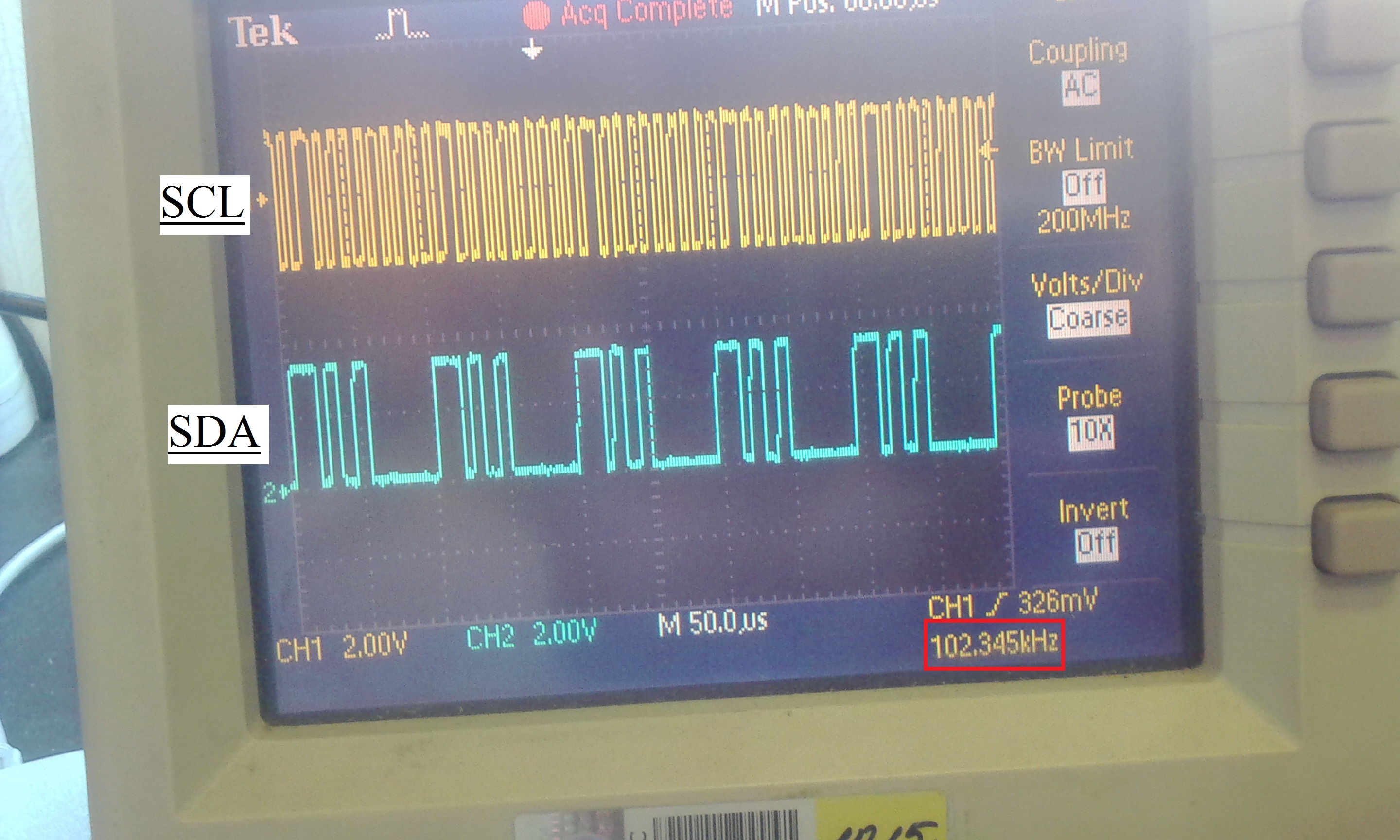
As I see, frequency of SCL (102.345kHz) is within limits of BQ32000(400kHz).
Communication also works, but it looks like controller repeats one message and BQ doesn`t take it.
Nevertheless, when I execute program step-by-step I can read data from RTC

Register I2CDRR shows 0x0005 when I2caRegs.I2CFFTX.bit.TXFFRST = 1; and becomes unchangeable while all further cycles of program.
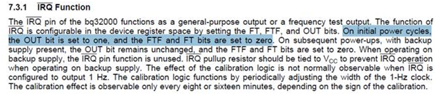
Also I tried to generate test signal of 512Hz from IRQ pin of BQ32000(according to pages 7-8 of datasheet)
But it remains in high level as on initial power cycles of device.

I am attaching both of my programs(I2C_RTC_bq32_tect – for test generation of 512 Hz signal from IRQ, I2C_RTC_bq32_write- load and read data from BQ32000)
Thanks for any help
Best regards,
Andrey
// TI File $Revision: /main/9 $
// Checkin $Date: August 10, 2007   09:05:58 $
//###########################################################################
//
// FILE:    Example_2833xI2c_rtc.c
//
// TITLE:   DSP2833x I2C RTC Example
//
// ASSUMPTIONS:
//
//    This program requires the DSP2833x header files.
//
//    This program requires an external I2C RTC connected to
//    the I2C bus at address 0x6f.
//
//    As supplied, this project is configured for "boot to SARAM"
//    operation.  The 2833x Boot Mode table is shown below.
//    For information on configuring the boot mode of an eZdsp,
//    please refer to the documentation included with the eZdsp,
//
//       $Boot_Table:
//
//         GPIO87   GPIO86     GPIO85   GPIO84
//          XA15     XA14       XA13     XA12
//           PU       PU         PU       PU
//        ==========================================
//            1        1          1        1    Jump to Flash
//            1        1          1        0    SCI-A boot
//            1        1          0        1    SPI-A boot
//            1        1          0        0    I2C-A boot
//            1        0          1        1    eCAN-A boot
//            1        0          1        0    McBSP-A boot
//            1        0          0        1    Jump to XINTF x16
//            1        0          0        0    Jump to XINTF x32
//            0        1          1        1    Jump to OTP
//            0        1          1        0    Parallel GPIO I/O boot
//            0        1          0        1    Parallel XINTF boot
//            0        1          0        0    Jump to SARAM       <- "boot to SARAM"
//            0        0          1        1    Branch to check boot mode
//            0        0          1        0    Boot to flash, bypass ADC cal
//            0        0          0        1    Boot to SARAM, bypass ADC cal
//            0        0          0        0    Boot to SCI-A, bypass ADC cal
//                                              Boot_Table_End$
//
// DESCRIPTION:
//
//    This program will write 1-14 words to RTC and read them back.
//    The data written and the RTC address written to are contained
//    in the message structure, I2cMsgOut1. The data read back will be
//    contained in the message structure I2cMsgIn1.
//
//    This program will work with the on-board I2C RTC supplied on
//    the F2833x eZdsp.
//
//
//###########################################################################
// Original Author: D.F.
//
// $TI Release: DSP2833x Header Files V1.01 $
// $Release Date: September 26, 2007 $
//###########################################################################


#include "DSP2833x_Device.h"     // DSP2833x Headerfile Include File
#include "DSP2833x_Examples.h"   // DSP2833x Examples Include File
// Note: I2C Macros used in this example can be found in the
// DSP2833x_I2C_defines.h file

// Prototype statements for functions found within this file.
void I2CA_Init(void);

Uint16 I2CA_WriteData(Uint16 addr, Uint16* buf, Uint16 len, Uint16 Start_Stop);


interrupt void i2c_int1a_isr(void);


///////  moe  ////////
Uint16 WaitI2C(void);
Uint16 CheckI2CLine(void);
/////// end moe ///////


#define I2C_SLAVE_ADDR       0xD0  //6f//
#define I2C_NUMBYTES          1
#define I2C_RNUMBYTES         8
#define I2C_RTC_HIGH_ADDR  0x00
//#define I2C_RTC_LOW_ADDR   0x30
#define I2C_RTC_LOW_ADDR   0x22
//#define START  I2caRegs.I2CMDR.all = 0x6E20;
//#define RTC_EN  GpioDataRegs.GPBCLEAR.bit.GPIO32=1;

Uint16 DATA[30];
Uint16  State_t, START;


void main(void)
{     Uint16 i;

// Step 1. Initialize System Control:
// PLL, WatchDog, enable Peripheral Clocks
// This example function is found in the DSP2833x_SysCtrl.c file.
   InitSysCtrl();

// Step 2. Initalize GPIO:
// This example function is found in the DSP2833x_Gpio.c file and
// illustrates how to set the GPIO to it's default state.
// InitGpio();
// Setup only the GP I/O only for I2C functionality
   InitI2CGpio();

// Step 3. Clear all interrupts and initialize PIE vector table:
// Disable CPU interrupts
   DINT;

// Initialize PIE control registers to their default state.
// The default state is all PIE interrupts disabled and flags
// are cleared.
// This function is found in the DSP2833x_PieCtrl.c file.
   InitPieCtrl();

// Disable CPU interrupts and clear all CPU interrupt flags:
   IER = 0x0000;
   IFR = 0x0000;
// Initialize the PIE vector table with pointers to the shell Interrupt
// Service Routines (ISR).
// This will populate the entire table, even if the interrupt
// is not used in this example.  This is useful for debug purposes.
// The shell ISR routines are found in DSP2833x_DefaultIsr.c.
// This function is found in DSP2833x_PieVect.c.
   InitPieVectTable();

// Interrupts that are used in this example are re-mapped to
// ISR functions found within this file.
   EALLOW;	// This is needed to write to EALLOW protected registers
   PieVectTable.I2CINT1A = &i2c_int1a_isr;
   EDIS;   // This is needed to disable write to EALLOW protected registers

// Step 4. Initialize all the Device Peripherals:
// This function is found in DSP2833x_InitPeripherals.c
   I2CA_Init();
   for(i=0;i<30;i++)
   {
       DATA[i]=0;
   }


/////////////////////////////////////////////////////// Step 5. User specific code

// Enable interrupts required for this example

// Enable I2C interrupt 1 in the PIE: Group 8 interrupt 1
   PieCtrlRegs.PIEIER8.bit.INTx1 = 1;// i2c -

// Enable CPU INT8 which is connected to PIE group 8
   IER |= M_INT8;
   EINT;
// ������
   DATA[0]=0;  	//  ����� �������� ��� ������
   DATA[1]=9;	//  ����� ������
   DATA[2]=5;
   for(;;)
   {
	   State_t=I2CA_WriteData(I2C_SLAVE_ADDR, DATA, 3, 0x6E20);
   }   // end of for(;;)
}   // end of main

void I2CA_Init(void)
{
   // Initialize I2C
	   I2caRegs.I2CMDR.all = 0x0000;	// Take I2C reset
	   									// Stop I2C when suspended

	   I2caRegs.I2CFFTX.all = 0x0000;	// Disable FIFO mode and TXFIFO
	   I2caRegs.I2CFFRX.all = 0x0040;	// Disable RXFIFO, clear RXFFINT,

	   #if (CPU_FRQ_150MHZ)             // Default - For 150MHz SYSCLKOUT
	        I2caRegs.I2CPSC.all = 14;   // Prescaler - need 7-12 Mhz on module clk (150/15 = 10MHz)
	   #endif
	   #if (CPU_FRQ_100MHZ)             // For 100 MHz SYSCLKOUT
	     I2caRegs.I2CPSC.all = 9;	    // Prescaler - need 7-12 Mhz on module clk (100/10 = 10MHz)
	   #endif

	   I2caRegs.I2CCLKL = 40;			// NOTE: must be non zero
	   I2caRegs.I2CCLKH = 42;			// NOTE: must be non zero
//	   	   I2caRegs.I2CIER.all = 0x24;		// Enable SCD & ARDY interrupts
//		   I2caRegs.I2CIER.bit.RRDY = 1;	// Data recieving ready
	   I2caRegs.I2CIER.all = 0;		//
//	   I2caRegs.I2CIER.bit.ARBL = 1;  	// Arbitrage lost
//	   I2caRegs.I2CIER.bit.NACK = 1;  	// no ACK
	   I2caRegs.I2CIER.bit.ARDY = 1;	// Registers ready for accsess
//	   I2caRegs.I2CIER.bit.RRDY = 1;	// Data recieving ready
//	   I2caRegs.I2CIER.bit.XRDY = 1;	// Data transmission ready
	   I2caRegs.I2CIER.bit.SCD = 1;		// Stop statment recieved
//	   I2caRegs.I2CIER.bit.AAS = 1;		// Adress as slave device
//
//	  I2caRegs.I2CFFTX.all = 0x6000;	// Enable FIFO mode and TXFIFO
//	  I2caRegs.I2CFFRX.all = 0x2040;	// Enable RXFIFO, clear RXFFINT,
		I2caRegs.I2CFFTX.all = 0; 			//I2C Transmit FIFO Register
		I2caRegs.I2CFFTX.bit.TXFFIL = 0; 	//set the transmit interrupt level (bit field TXFFIL) to zero
		I2caRegs.I2CFFTX.bit.I2CFFEN = 1; 	//Enable the FIFOs
		I2caRegs.I2CFFTX.bit.TXFFRST = 1; 	//Enable the FIFO-transmit support

		I2caRegs.I2CFFRX.all = 0; 			//I2C Receive FIFO Register
		I2caRegs.I2CFFRX.bit.RXFFIL = 2; 	//set the receive interrupt level (bit field RXFFIL) to 2, because we will receive a 2 byte temperature message from the TMP100
		I2caRegs.I2CFFRX.bit.RXFFRST = 1; 	//Enable the FIFO-receiver support

		I2caRegs.I2CFFRX.bit.RXFFIENA = 1; 	//enable interrupt after receiving two temperature bytes from the TMP100

		   									// Stop I2C when suspended
		I2caRegs.I2CMDR.bit.IRS = 1;	// Take I2C out of reset

}
Uint16 I2CA_WriteData(Uint16 AddrSlave, Uint16 *buffer, Uint16 len, Uint16 START_STOP)
{   int ii=0;
	START=START_STOP;//0x6E20;

	I2caRegs.I2CMDR.bit.IRS = 1;                // reset I2C

	while(CheckI2CLine()); // Make sure I2C is not busy and has stopped

    I2caRegs.I2CSAR = AddrSlave;                     // I2C slave address
    I2caRegs.I2CCNT = len;
	for(;ii< len ;ii++)
	{
      I2caRegs.I2CDXR = *(buffer+ii);
	}
   I2caRegs.I2CMDR.all = START_STOP; // start, stop, no rm, reset i2c  01101110 00100000
	if (WaitI2C()) return;


}

interrupt void i2c_int1a_isr(void)     // I2C-A
{
   Uint16 IntSource, i;

   // Read interrupt source
   IntSource = I2caRegs.I2CISRC.all;
   switch (IntSource) {
	case I2C_ARB_ISRC:  // Arbitrage lost condition   ---- I2CSTR.AL

		break;
	case I2C_NACK_ISRC:  // NACK condition  ---- I2CSTR.NACK
		I2caRegs.I2CMDR.bit.STP = 1; // send STP to end transfer
		I2caRegs.I2CSTR.bit.NACK = 1; // clear NACK bit
//		I2C_Comm_Error++;
		break;
	case I2C_ARDY_ISRC:  // ARDY condition ---- I2CSTR.ARDY
//	      if(I2caRegs.I2CSTR.bit.NACK == 1)
//	      {
	     I2caRegs.I2CMDR.all=START;
//	    			  I2caRegs.I2CMDR.bit.STP = 1;
//	         I2caRegs.I2CSTR.all = I2C_CLR_NACK_BIT;
//	      }
	 		break;
	case I2C_RX_ISRC:  // data accsepted I2CSTR.RRDY
		if (I2caRegs.I2CFFRX.bit.RXFFINT == 1) // RX-FIFO - interrupt
		{  	for (i=0;i<I2caRegs.I2CCNT;i++)
    		{
			DATA[i] = I2caRegs.I2CDRR;
    		}
			//DATA[1] = I2caRegs.I2CDRR ;
			I2caRegs.I2CFFRX.bit.RXFFINTCLR = 1; // clear ISR
		}
		break;
	case I2C_TX_ISRC:  // Data transmitted I2CSTR.XRDY
		if (I2caRegs.I2CFFTX.bit.TXFFINT == 1) // RX-FIFO - interrupt
		I2caRegs.I2CFFTX.bit.TXFFINTCLR = 1;
		I2caRegs.I2CISRC.all=1;
		break;
	case I2C_SCD_ISRC:  // STOP condition found ---- I2CSTR.SCD
		I2caRegs.I2CSTR.bit.SCD=1;

		break;
	case I2C_AAS_ISRC:  // MASTER as a SLAVE condition found---- I2CSTR.AAS
		break;

	default:
		break;
}
   PieCtrlRegs.PIEACK.all = PIEACK_GROUP8;
}
Uint16 CheckI2CLine(void)
{
   if (I2caRegs.I2CMDR.bit.STP == 1)
   {
	  //ECode.ECode1.bit.eI2C=1;
      return 1;
   }
   if (I2caRegs.I2CSTR.bit.BB == 1)
   {
	//  ECode.ECode1.bit.eI2C=1; // Error flag
      return 1;
   }
   return 0;
}
Uint16 WaitI2C(void)
{
    int timer = 0x05ff;

	/* Check for I2C INT for completion */
    while (--timer)
      if (I2caRegs.I2CMDR.bit.STP ==0) break;

    if (timer)
    {
//	  ECode.ECode1.bit.eI2C = 0;  // Error flag
	  return 0;
    }
    else
    {
	  //ECode.ECode1.bit.eI2C = 1; // Error flag
	  return 1;
    }
	}

void InitI2CGpio(void)
{

	   EALLOW;
	/* Enable internal pull-up for the selected pins */
	// Pull-ups can be enabled or disabled disabled by the user.
	// This will enable the pullups for the specified pins.
	// Comment out other unwanted lines.
		GpioCtrlRegs.GPBPUD.bit.GPIO32 = 0;    // Enable pull-up for GPIO32 (SDAA)
		GpioCtrlRegs.GPBPUD.bit.GPIO33 = 0;	   // Enable pull-up for GPIO33 (SCLA)

	/* Set qualification for selected pins to asynch only */
	// This will select asynch (no qualification) for the selected pins.
	// Comment out other unwanted lines.
	//	GpioCtrlRegs.GPBQSEL1.all=0;
		GpioCtrlRegs.GPBQSEL1.bit.GPIO32 = 3;  // Asynch input GPIO32 (SDAA)
	    GpioCtrlRegs.GPBQSEL1.bit.GPIO33 = 3;  // Asynch input GPIO33 (SCLA)

	/* Configure SCI pins using GPIO regs*/
	// This specifies which of the possible GPIO pins will be I2C functional pins.
	// Comment out other unwanted lines.
	 //   GpioCtrlRegs.GPBMUX1.all=0;
		GpioCtrlRegs.GPBMUX1.bit.GPIO32 = 1;   // Configure GPIO32 for SDAA operation
		GpioCtrlRegs.GPBMUX1.bit.GPIO33 = 1;   // Configure GPIO33 for SCLA operation
/*		GpioCtrlRegs.GPBMUX1.bit.GPIO32 = 0;//1;   // Configure GPIO32 for SDAA operation
		GpioCtrlRegs.GPBMUX1.bit.GPIO33 = 0;//1;   // Configure GPIO33 for SCLA operation
		GpioCtrlRegs.GPBDIR.bit.GPIO32=1;
		GpioCtrlRegs.GPBDIR.bit.GPIO33=1;*/
	    EDIS;

}

//===========================================================================
// No more.
//===========================================================================
// TI File $Revision: /main/9 $
// Checkin $Date: August 10, 2007   09:05:58 $
//###########################################################################
//
// FILE:    Example_2833xI2c_rtc.c
//
// TITLE:   DSP2833x I2C RTC Example
//
// ASSUMPTIONS:
//
//    This program requires the DSP2833x header files.
//
//    This program requires an external I2C RTC connected to
//    the I2C bus at address 0x6f.
//
//    As supplied, this project is configured for "boot to SARAM"
//    operation.  The 2833x Boot Mode table is shown below.
//    For information on configuring the boot mode of an eZdsp,
//    please refer to the documentation included with the eZdsp,
//
//       $Boot_Table:
//
//         GPIO87   GPIO86     GPIO85   GPIO84
//          XA15     XA14       XA13     XA12
//           PU       PU         PU       PU
//        ==========================================
//            1        1          1        1    Jump to Flash
//            1        1          1        0    SCI-A boot
//            1        1          0        1    SPI-A boot
//            1        1          0        0    I2C-A boot
//            1        0          1        1    eCAN-A boot
//            1        0          1        0    McBSP-A boot
//            1        0          0        1    Jump to XINTF x16
//            1        0          0        0    Jump to XINTF x32
//            0        1          1        1    Jump to OTP
//            0        1          1        0    Parallel GPIO I/O boot
//            0        1          0        1    Parallel XINTF boot
//            0        1          0        0    Jump to SARAM       <- "boot to SARAM"
//            0        0          1        1    Branch to check boot mode
//            0        0          1        0    Boot to flash, bypass ADC cal
//            0        0          0        1    Boot to SARAM, bypass ADC cal
//            0        0          0        0    Boot to SCI-A, bypass ADC cal
//                                              Boot_Table_End$
//
// DESCRIPTION:
//
//    This program will write 1-14 words to RTC and read them back.
//    The data written and the RTC address written to are contained
//    in the message structure, I2cMsgOut1. The data read back will be
//    contained in the message structure I2cMsgIn1.
//
//    This program will work with the on-board I2C RTC supplied on
//    the F2833x eZdsp.
//
//
//###########################################################################
// Original Author: D.F.
//
// $TI Release: DSP2833x Header Files V1.01 $
// $Release Date: September 26, 2007 $
//###########################################################################


#include "DSP2833x_Device.h"     // DSP2833x Headerfile Include File
#include "DSP2833x_Examples.h"   // DSP2833x Examples Include File
// Note: I2C Macros used in this example can be found in the
// DSP2833x_I2C_defines.h file

// Prototype statements for functions found within this file.
void I2CA_Init(void);
interrupt void i2c_int1a_isr(void);


///////  moe  ////////
Uint16 WaitI2C(void);
Uint16 CheckI2CLine(void);
/////// end moe ///////


#define I2C_SLAVE_ADDR       0xD0  //6f//
#define I2C_NUMBYTES          1
#define I2C_RNUMBYTES         8
#define I2C_RTC_HIGH_ADDR  0x00
//#define I2C_RTC_LOW_ADDR   0x30
#define I2C_RTC_LOW_ADDR   0x22
//#define START  I2caRegs.I2CMDR.all = 0x6E20;
//#define RTC_EN  GpioDataRegs.GPBCLEAR.bit.GPIO32=1;

Uint16  DATA[30];
Uint16  START;

void main(void)
{
// Step 1. Initialize System Control:
// PLL, WatchDog, enable Peripheral Clocks
// This example function is found in the DSP2833x_SysCtrl.c file.
   InitSysCtrl();

// Step 2. Initalize GPIO:
// This example function is found in the DSP2833x_Gpio.c file and
// illustrates how to set the GPIO to it's default state.
// InitGpio();
// Setup only the GP I/O only for I2C functionality
   InitI2CGpio();

// Step 3. Clear all interrupts and initialize PIE vector table:
// Disable CPU interrupts
   DINT;

// Initialize PIE control registers to their default state.
// The default state is all PIE interrupts disabled and flags
// are cleared.
// This function is found in the DSP2833x_PieCtrl.c file.
   InitPieCtrl();

// Disable CPU interrupts and clear all CPU interrupt flags:
   IER = 0x0000;
   IFR = 0x0000;
// Initialize the PIE vector table with pointers to the shell Interrupt
// Service Routines (ISR).
// This will populate the entire table, even if the interrupt
// is not used in this example.  This is useful for debug purposes.
// The shell ISR routines are found in DSP2833x_DefaultIsr.c.
// This function is found in DSP2833x_PieVect.c.
   InitPieVectTable();

// Interrupts that are used in this example are re-mapped to
// ISR functions found within this file.
   EALLOW;	// This is needed to write to EALLOW protected registers
   PieVectTable.I2CINT1A = &i2c_int1a_isr;
   EDIS;   // This is needed to disable write to EALLOW protected registers

// Step 4. Initialize all the Device Peripherals:
// This function is found in DSP2833x_InitPeripherals.c
  I2CA_Init();

// Step 5. User specific code

// Enable interrupts required for this example

// Enable I2C interrupt 1 in the PIE: Group 8 interrupt 1
   PieCtrlRegs.PIEIER8.bit.INTx1 = 1;// i2c -

// Enable CPU INT8 which is connected to PIE group 8
   IER |= M_INT8;
   EINT;


//////////////////////////////////////////////////////////////////////////Step 5. User specific code

// test configuration OUT=1 � FT=1    IRQ---512 Hz
   	   START=0x6E20; // bit FREE + STT + STP + MST + TRX + IRS
   	   I2caRegs.I2CSAR = I2C_SLAVE_ADDR;
	   I2caRegs.I2CCNT = 2;
	   I2caRegs.I2CDXR = 0x07;  // CAL_CFG1 Register
	   I2caRegs.I2CDXR = 0xC0;  //  bit OUT=1 and bit FT=1
	   I2caRegs.I2CMDR.all = START;
	if (WaitI2C()) return;
   for(;;)
   {

   }   // end of for(;;)
}   // end of main

void I2CA_Init(void)
{
   // Initialize I2C
	   I2caRegs.I2CMDR.all = 0x0000;	// Take I2C reset
	   									// Stop I2C when suspended

	   I2caRegs.I2CFFTX.all = 0x0000;	// Disable FIFO mode and TXFIFO
	   I2caRegs.I2CFFRX.all = 0x0040;	// Disable RXFIFO, clear RXFFINT,

	   #if (CPU_FRQ_150MHZ)             // Default - For 150MHz SYSCLKOUT
	        I2caRegs.I2CPSC.all = 14;   // Prescaler - need 7-12 Mhz on module clk (150/15 = 10MHz)
	   #endif
	   #if (CPU_FRQ_100MHZ)             // For 100 MHz SYSCLKOUT
	     I2caRegs.I2CPSC.all = 9;	    // Prescaler - need 7-12 Mhz on module clk (100/10 = 10MHz)
	   #endif

	   I2caRegs.I2CCLKL = 40;			// NOTE: must be non zero
	   I2caRegs.I2CCLKH = 42;			// NOTE: must be non zero
//	   	   I2caRegs.I2CIER.all = 0x24;		// Enable SCD & ARDY interrupts
//		   I2caRegs.I2CIER.bit.RRDY = 1;	// Data recieving ready
	   I2caRegs.I2CIER.all = 0;		//
//	   I2caRegs.I2CIER.bit.ARBL = 1;  	// Arbitrage lost
//	   I2caRegs.I2CIER.bit.NACK = 1;  	// no ACK
	   I2caRegs.I2CIER.bit.ARDY = 1;	// Registers ready for accsess
//	   I2caRegs.I2CIER.bit.RRDY = 1;	// Data recieving ready
//	   I2caRegs.I2CIER.bit.XRDY = 1;	// Data transmission ready
	   I2caRegs.I2CIER.bit.SCD = 1;		// Stop statment recieved
//	   I2caRegs.I2CIER.bit.AAS = 1;		// Adress as slave device
//
//	  I2caRegs.I2CFFTX.all = 0x6000;	// Enable FIFO mode and TXFIFO
//	  I2caRegs.I2CFFRX.all = 0x2040;	// Enable RXFIFO, clear RXFFINT,
		I2caRegs.I2CFFTX.all = 0; 			//I2C Transmit FIFO Register
		I2caRegs.I2CFFTX.bit.TXFFIL = 0; 	//set the transmit interrupt level (bit field TXFFIL) to zero
		I2caRegs.I2CFFTX.bit.I2CFFEN = 1; 	//Enable the FIFOs
		I2caRegs.I2CFFTX.bit.TXFFRST = 1; 	//Enable the FIFO-transmit support

		I2caRegs.I2CFFRX.all = 0; 			//I2C Receive FIFO Register
		I2caRegs.I2CFFRX.bit.RXFFIL = 2; 	//set the receive interrupt level (bit field RXFFIL) to 2, because we will receive a 2 byte temperature message from the TMP100
		I2caRegs.I2CFFRX.bit.RXFFRST = 1; 	//Enable the FIFO-receiver support

		I2caRegs.I2CFFRX.bit.RXFFIENA = 1; 	//enable interrupt after receiving two temperature bytes from the TMP100

		   									// Stop I2C when suspended
		I2caRegs.I2CMDR.bit.IRS = 1;	// Take I2C out of reset

}

interrupt void i2c_int1a_isr(void)     // I2C-A
{
   Uint16 IntSource, i;

   // Read interrupt source
   IntSource = I2caRegs.I2CISRC.all;
   switch (IntSource) {
	case I2C_ARB_ISRC:                       // Arbitrage lost condition   ---- I2CSTR.AL

		break;
	case I2C_NACK_ISRC:                     // NACK condition  ---- I2CSTR.NACK
		I2caRegs.I2CMDR.bit.STP = 1; // send STP to end transfer
		I2caRegs.I2CSTR.bit.NACK = 1; // clear NACK bit
//		I2C_Comm_Error++;
		break;
	case I2C_ARDY_ISRC:                    // ARDY condition ---- I2CSTR.ARDY
//	      if(I2caRegs.I2CSTR.bit.NACK == 1)
//	      {
	     I2caRegs.I2CMDR.all=START;
//	    			  I2caRegs.I2CMDR.bit.STP = 1;
//	         I2caRegs.I2CSTR.all = I2C_CLR_NACK_BIT;
//	      }
	 		break;
	case I2C_RX_ISRC:                    // Data accsepted I2CSTR.RRDY
		if (I2caRegs.I2CFFRX.bit.RXFFINT == 1) // RX-FIFO - interrupt
		{  	for (i=0;i<I2caRegs.I2CCNT;i++)
    		{
			DATA[i] = I2caRegs.I2CDRR;
    		}
			//DATA[1] = I2caRegs.I2CDRR ;
			I2caRegs.I2CFFRX.bit.RXFFINTCLR = 1; // clear ISR
		}
		break;
	case I2C_TX_ISRC:  // Data transmitted I2CSTR.XRDY
		if (I2caRegs.I2CFFTX.bit.TXFFINT == 1) // RX-FIFO - interrupt
		I2caRegs.I2CFFTX.bit.TXFFINTCLR = 1;
		I2caRegs.I2CISRC.all=1;
		break;
	case I2C_SCD_ISRC:  // STOP condition found ---- I2CSTR.SCD
		I2caRegs.I2CSTR.bit.SCD=1;

		break;
	case I2C_AAS_ISRC:  // MASTER as a SLAVE condition found---- I2CSTR.AAS
		break;

	default:
		break;
}
   PieCtrlRegs.PIEACK.all = PIEACK_GROUP8;
}
Uint16 CheckI2CLine(void)
{
   if (I2caRegs.I2CMDR.bit.STP == 1)
   {
      return 1;
   }
   if (I2caRegs.I2CSTR.bit.BB == 1)
   {
      return 1;
   }
   return 0;
}
Uint16 WaitI2C(void)
{
    int timer = 0x05ff;

	/* Check for I2C INT for completion */
    while (--timer)
      if (I2caRegs.I2CMDR.bit.STP ==0) break;

    if (timer)
    {
	  return 0;
    }
    else
    {
	  return 1;
    }
	}

void InitI2CGpio(void)
{

	   EALLOW;
	/* Enable internal pull-up for the selected pins */
	// Pull-ups can be enabled or disabled disabled by the user.
	// This will enable the pullups for the specified pins.
	// Comment out other unwanted lines.
		GpioCtrlRegs.GPBPUD.bit.GPIO32 = 0;    // Enable pull-up for GPIO32 (SDAA)
		GpioCtrlRegs.GPBPUD.bit.GPIO33 = 0;	   // Enable pull-up for GPIO33 (SCLA)

	/* Set qualification for selected pins to asynch only */
	// This will select asynch (no qualification) for the selected pins.
	// Comment out other unwanted lines.
	//	GpioCtrlRegs.GPBQSEL1.all=0;
		GpioCtrlRegs.GPBQSEL1.bit.GPIO32 = 3;  // Asynch input GPIO32 (SDAA)
	    GpioCtrlRegs.GPBQSEL1.bit.GPIO33 = 3;  // Asynch input GPIO33 (SCLA)

	/* Configure SCI pins using GPIO regs*/
	// This specifies which of the possible GPIO pins will be I2C functional pins.
	// Comment out other unwanted lines.
	 //   GpioCtrlRegs.GPBMUX1.all=0;
		GpioCtrlRegs.GPBMUX1.bit.GPIO32 = 1;   // Configure GPIO32 for SDAA operation
		GpioCtrlRegs.GPBMUX1.bit.GPIO33 = 1;   // Configure GPIO33 for SCLA operation
/*		GpioCtrlRegs.GPBMUX1.bit.GPIO32 = 0;//1;   // Configure GPIO32 for SDAA operation
		GpioCtrlRegs.GPBMUX1.bit.GPIO33 = 0;//1;   // Configure GPIO33 for SCLA operation
		GpioCtrlRegs.GPBDIR.bit.GPIO32=1;
		GpioCtrlRegs.GPBDIR.bit.GPIO33=1;*/
	    EDIS;

}

//===========================================================================
// No more.
//===========================================================================
