This thread has been locked.

If you have a related question, please click the "Ask a related question" button in the top right corner. The newly created question will be automatically linked to this question.

Nonlinear F2833x Internal ADC Performance

Other Parts Discussed in Thread: TMS320F28235

We are struggling to figure out the why the internal ADC in the TMS320F28235 can not achieve a linear  transfer function (0-3.0V) -> (0-65535) .  Best case we can get 0.5% (327 dword) , which is well above the specified INL of 2 bits.  The graph shows that at around 2.4-3.0V the error skyrockets.  The plot already applies the best fit gain/offset compensation.  I have also attached our initialization code.  ADC sequencing was turned off so that only the channel in question is being measured.  Thanks for your input!

// Set Analog as Inputs
InitAdc();
AdcRegs.ADCTRL1.bit.ACQ_PS = ADC_SHCLK;
AdcRegs.ADCTRL1.bit.SEQ_CASC = 1; // disable other channels for testing purposes
AdcRegs.ADCTRL3.bit.ADCCLKPS = ADC_CKPS;
AdcRegs.ADCMAXCONV.bit.MAX_CONV1 = 0;
AdcRegs.ADCCHSELSEQ1.bit.CONV00 = 0;  /* Setup conv from ADCINA0 and ADCINB0 */
AdcRegs.ADCCHSELSEQ1.bit.CONV01 = 1;  /* Setup conv from ADCINA1 and ADCINB1 */
AdcRegs.ADCCHSELSEQ1.bit.CONV02 = 2;  /* Setup conv from ADCINA2 and ADCINB2 */
AdcRegs.ADCCHSELSEQ1.bit.CONV03 = 3;  /* Setup conv from ADCINA3 and ADCINB3 */
AdcRegs.ADCTRL1.bit.CONT_RUN = 1;
AdcRegs.ADCTRL2.bit.SOC_SEQ1 = 1; // Start of conversion trigger for SEQ1
AdcRegs.ADCREFSEL.bit.REF_SEL = 0;

  • Hi Grant,

    What is the source into the ADC? If it is a function generator, are you sure the range isn't changing when the output voltage exceeds ~2.1V?
  • I am using a Rigol dc power supply and validating the output using a Fluke multi meter. The supply matches up to 0.01% over the full range. Our target accuracy is also 0.01%, which is pretty standard in the power supply industry (we make power supplies too!). 

  • Hi Grant,

    Does the signal get buffered on the board near the ADC input? An op-amp would be ideal, but you could also use a large capacitor (>> 4 x 4096 x Ch, which I think is around 50nF ). If using a large capacitor, note that you may need to use a slower sampling rate than maximum as the charge can potentially get drained off of the external cap. by the inrush current into Ch from each sample.

    Are you taking a single ADC sample at each point, or an average of many samples? Recording the raw result for multiple samples can be useful too (instead of only taking the average) because it gives you an idea of the noise is present on the input. You can also see if there is a difference between the first and subsequent samples (which could indicate an input settling issue).

    Configuration wise, it would be good to check the ADC clock settings - the ADC should be clocked at no more than 25MHz.

    Are you using a custom board, or a TI kit? A good thing to double check would be that the components on the reference pins are correctly populated (22k on ADCRESEXT, and 2.2uF on ADCREFP and ADCREFM)?
  • Devin,

    In ADC initialize code posted at the top I thought I disabled sequencing (line 4).  I was hoping this would keep the analog MUX connected to the ADC and eliminate the possibility of capacitor charging as a problem.  The amplifier stage is shown below (custom board). I verified that the attenuation for the op amp transfer function, input voltage (0-10V) to output voltage (0-3V), was linear and 0.01% accurate and the problem is localized to the ADC conversion process. The input capacitance for the ADC channel is 0.1uF.  

    I will go through my settings and post my sample rate and and ADC clock settings.  I will try lowering them while I wait for you next set of recommendations.

    The ADC pin connections was configured for external reference, but we are using the internal reference(we recently discovered only three reference voltages are supported).  I cut the trace leaving ADCREFIN and grounded the ADCREFIN pin, per the recommendation of the datasheet.

    I agree that averaging samples will help eliminate noise, but I have repeated the experiment 3-4 times and the error vs. input voltage curve has been the same. I I do not believe averaging the samples will have any effect.  If you need me to post more detailed measurements let me know.

  • The clock was set for 12.5MHz, I went ahead and changed the clock and the sample hold window it to the largest divisor and nonlinear  error is now gone.   I will make the firmware changes then send our board out for qualification.  Should be fixed.  Thanks for the help.

    #define ADC_CKPS   0xF   // ADC module clock = HSPCLK/30*ADC_CKPS   25.0MHz/(30*15) = 15.5kHz
    #define ADC_SHCLK  0xF   // S/H width in ADC module periods

    I went ahead and changed the clock for 

  • Hi Grant,

    Glad you were able to find a workaround.  I think we can probably explain this behavior:

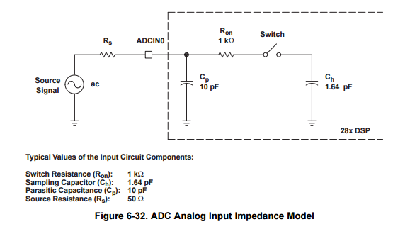
    The ADC will always close the S+H switch only for the duration of the S+H window (even if channels aren't changing between conversions) and this will usually result in some current flow in (or out) of the ADC input as the external driver and external capacitance equalize with the internal ADC channel capacitance.

    The ADC input looks like this:


    The effective Rs for your voltage divider is 7.5k || 2.49k = 1870.

    Cp is 100nF + 10pf = 100nF.

    We can use the formula (rs + ron)*Ch + Rs*Cp to get the time constant for settling on Ch. This gives 187us. To settle to within 1/4LSBs (typically how we define ideal settling) you need -ln((1/4096)*(1/4)) time constants = 9.7 time constants.  Therefore the required settling time is 1.8ms! 

    This is much larger than anything you could set the S+H window too, but if we assume the external capacitor is fully charged when the ADC samples we can ignore the impedance of the voltage divider.  If we want the ADC to settle to about 1/4LSBs just via charge equalization with the external capacitor, then we need an external capacitor that is at least Ch * 4096 * 4 = 1.6pF * 4096 * 4 = 26nF. We meet this criteria, so we should actually be ok even using the minimum S+H window.

    Now if the voltage on the external cap drops by 1/4 LSB each time we sample, it won't stay fully charged forever.  The external op-amp will recharge the external capacitor, but this is subject to the impedance of Rs.  If we relax the allowable error to 1/2 LSBs on Ch, then at the beginning of the sample the external capacitor can be within 1/4LSBs of its final value (whatever the op-amp is driving it to) and then the sample will drain it to within 1/2LSBs.  The op-amp then needs to recharge it to 1/4LSBs in the time between samples.  This is half way from its starting point to its ideal point, so the number of time constants needed is -ln(0.5) = 0.7.  The external time constant is Rs*Cp = 187us, so the time between samples has to be longer than 187us * 0.7 = 131us.  This means the sampling rate can be no higher than 1/131us = 7.6kHz. 

    The above assumes the worst case that the ADC s+h capacitor, Ch, starts completely discharged.  If this was the case, you would experience the settling error as an attenuation of the input signal, which wouldn't give you the non-linearity you are seeing.  In reality, there is some voltage leftover on the capacitor after a sample that is dependent on the ADC architecture, the previously converted voltage, and how long ago the previous voltage was converted.  You can try to remove this factor by sampling ground before your real conversion.  However a much better solution would be to reduce the sample rate or to reduce the input impedance driving the ADC input.