Because of the holidays, TI E2E™ design support forum responses will be delayed from Dec. 25 through Jan. 2. Thank you for your patience.

This thread has been locked.

If you have a related question, please click the "Ask a related question" button in the top right corner. The newly created question will be automatically linked to this question.

F28377 EMIF to SDRAM hardware configuration

Other Parts Discussed in Thread: CONTROLSUITE

Hi,

  I want to use the F28377 EMIF to control the SDRAM.

  Now I want to make sure the whether the hardware configuration is correct.

1.SDRAM selection

I choose the SDRAM with parameters below as reference.

Type: SDRAM

Data bus width: 16 bit

Supply voltage:3.3V

Organizition: 4/8/16/32M * 16 (I think these are compatible and can be replaced depend on the capacity demand. Is that right? )

But I don't know how to deal with the Maximum Clock Frequency and Access Time.

The Sysclk of F28377D is 200MHz and does it means I must use  the SDRAM maximum clock frequency at 200MHz?

And how to choose the SDRAM depend on the Access Time?

I select the SDRAM from MOUSER.

2.Hardware connection

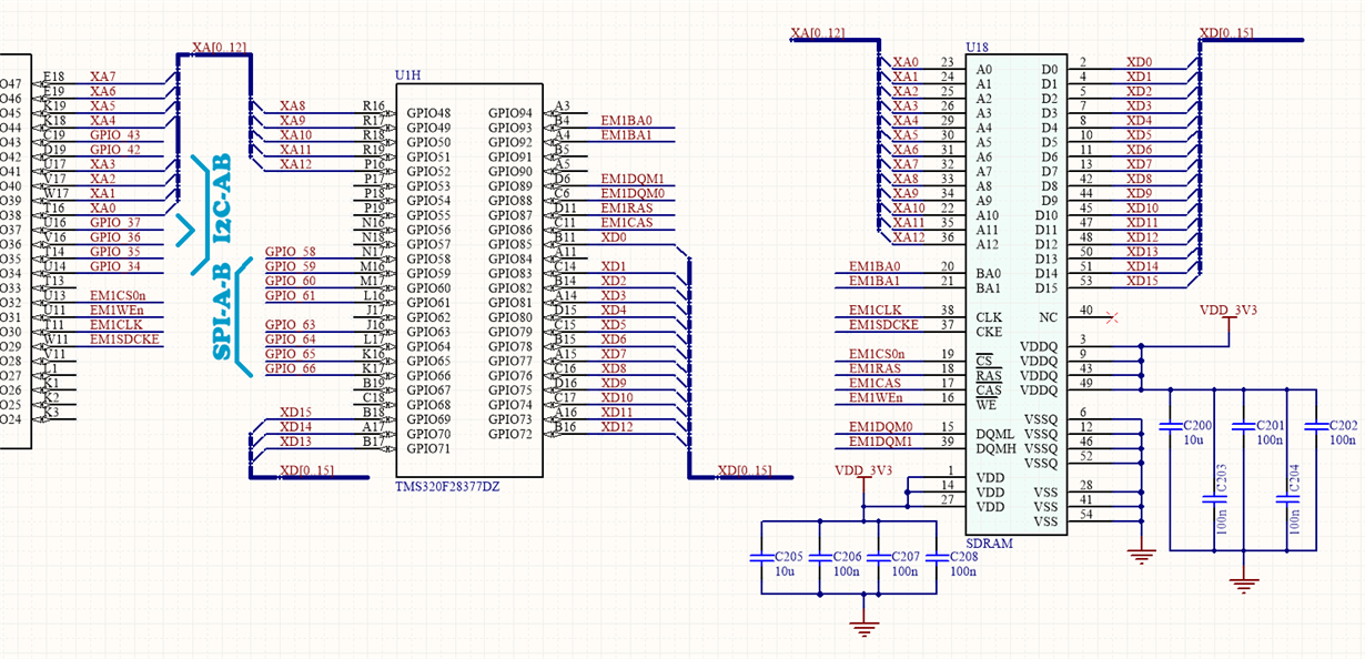
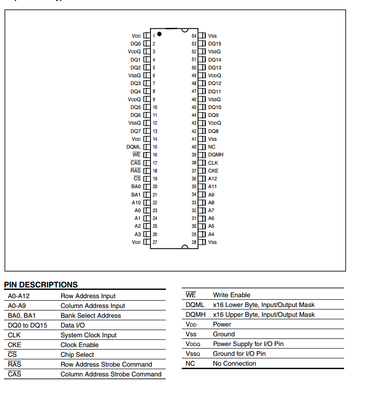
Take the IS42S16320D-7TLI as a example.

I want to know whether the hardware connection is correct.

IO settings:

GPIO 38-41,44-52 as the 13 bit address line;

GPIO 69-83,85 as the 16 bit data line;

GPIO 29 30 31 32 as EMIF SDCKE CLK WE CS0;

GPIO 86 87 AS CAS RAS;

GPIO 88 89 as DQM0 DQM1(DQM0 for DQML x16 Lower Byte, Input/Output Mask, DQM1 for DQMH x16 Upper Byte, Input/Output Mask)

GPIO 92 93 as BA0 BA1;

Is there some examples from TI that show the hardware settings for EMIF to SDRAM?

Looking forward to your reply!

Best regards,

Di

  • Hi,

    Organizition: 4/8/16/32M * 16 (I think these are compatible and can be replaced depend on the capacity demand. Is that right? )

    That's correct. Just make sure no of banks are ok.

    The Sysclk of F28377D is 200MHz and does it means I must use  the SDRAM maximum clock frequency at 200MHz?

    SDRAM interface can work at max 100MHz on this device. PERCLKDIVSEL register has configuration bit to divide the SYSCLK for EMIF.

    And how to choose the SDRAM depend on the Access Time?

    SDRAM is synchronous interface and all the input/output have timing wrt CLK. This information is available in device datasheet. Please refer that and make sure these values are within range of external device you are choosing.

    Is there some examples from TI that show the hardware settings for EMIF to SDRAM?

    controlSUITE has multiple SDRAM examples (emif1_16bit_sdram_dma, emif1_16bit_sdram_far) which you can refer for the settings.

    Regards,

    Vivek Singh

  • Hi Vivek,

      Thanks for your nice reply!

      I checked the SDRAM examples (emif1_16bit_sdram_far) and compared the IO settings with my schematic.

      There are some differences as below. 

    1.

    // GPIO33 -- External memory interface 1 read not write

    I don't know the function of this IO.

    2.

    // GPIO34 -- External memory interface 1 chip select 2
    // GPIO35 -- External memory interface 1 chip select 3

    I think these CS2-4 are used for Asynchronous Memory. 

    Are they necessary for SDRAM?

    3.


    // GPIO36 -- External memory interface 1 Asynchronous SRAM WAIT

    I think it's also a IO for Asynchronous Memory.

    4.
    // GPIO37 -- External memory interface 1 output enable

    I don't know the function of this IO.

    5.

    // GPIO90 -- External memory interface 1 Input/output mask for byte 2
    // GPIO91 -- External memory interface 1 Input/output mask for byte 3

    I think these pins are used for 32 bits data bus width SDRAM.

    I checked and compared the IO initialization codes and marked the IO I used with a '-' in the comments.

    void setup_emif1_pinmux_sdram_16bit(Uint16 cpu_sel)
    {
    	int i;
    
    	// -GPIO29 -- External memory interface 1 SDRAM clock enable
    	// -GPIO30 -- External memory interface 1 clock
    	// -GPIO31 -- External memory interface 1 write enable
    	// -GPIO32 -- External memory interface 1 chip select 0
    	// GPIO33 -- External memory interface 1 read not write
    	// GPIO34 -- External memory interface 1 chip select 2
    	// GPIO35 -- External memory interface 1 chip select 3
    	// GPIO36 -- External memory interface 1 Asynchronous SRAM WAIT
    	// GPIO37 -- External memory interface 1 output enable
    	// -GPIO38-41 -- External memory interface 1 address line 0-3
    	// -GPIO44-52 -- External memory interface 1 address line 4-12
        
    	for (i=29; i<=52;i++) 
        {
            if (i != 42 || i != 43)
            {        
                GPIO_SetupPinMux(i,cpu_sel,2);
            }
    	}
    	
    	// -GPIO69-83 -- External memory interface 1 data line 15-1
    	// -GPIO85 -- External memory interface 1 data line 0
        
    	for (i=69; i<=85;i++) 
        {
            if (i != 84)
            {
                GPIO_SetupPinMux(i,cpu_sel,2);
            }
    	}
    	
    	// -GPIO86 -- External memory interface 1 column address strobe
    	// -GPIO87 -- External memory interface 1 row address strobe
    	// -GPIO88 -- External memory interface 1 Input/output mask for byte 0
    	// -GPIO89 -- External memory interface 1 Input/output mask for byte 1
    	// GPIO90 -- External memory interface 1 Input/output mask for byte 2
    	// GPIO91 -- External memory interface 1 Input/output mask for byte 3
    	// -GPIO92 -- External memory interface 1 bank address 1
    	// -GPIO93 -- External memory interface 1 bank address 0
    	
    	for(i=86;i<=93;i++)
        {
    	   GPIO_SetupPinMux(i,cpu_sel,3);
    	}
    
    	//configure Data pins for Async mode
    	for (i = 69;i <= 85;i++)
        {
    		if (i != 84)
            {
    			GPIO_SetupPinOptions(i,0,0x31);
            }
    	}
    
    	GPIO_SetupPinOptions(88,0,0x31);
    	GPIO_SetupPinOptions(89,0,0x31);
    	GPIO_SetupPinOptions(90,0,0x31);
    	GPIO_SetupPinOptions(91,0,0x31);
    }
    
    void setup_emif2_pinmux_sdram_16bit(Uint16 cpu_sel)
    {
    	int i;
        
    	for (i=53; i<=68;i++) 
        {
            GPIO_SetupPinMux(i,cpu_sel,3);
    	}
    	for (i=96; i<=121;i++) 
        {
            GPIO_SetupPinMux(i,cpu_sel,3);
    	}
    	
    	//configure Data pins for Async mode
    	for (i = 53;i <= 68;i++)
        {
            GPIO_SetupPinOptions(i,0,0x31);
    	}
    }
    

    Could you please check the differences?

    Thanks a lot.

    Di


  • Hi Vivek,

      Sorry to bother you again.

      I installed the Controlsuite and have gotten many useful examples from it.

      I want to know is there some hardware design examples with F28377.

      I think it would be very helpful if I can get the schematic example for F28377 EMIF to SDRAM then I would know how to choose a SDRAM and how to connect the F28377 with the SDRAM via EMIF.

      I really hope you would help me check the hardware connection and then I can start the software learning.

      Thanks again for your nice reply.

      I have learned a lot from E2E as a student and thanks everyone here!

      Best regards,

      Di

  • Hi Jiao, Sorry, look like I missed replying to this post because this was closed. I hope you were able to get it working. We do not have reference design for this to share with customer since this is standard interface.
    Regards,
    Vivek Singh