This thread has been locked.

If you have a related question, please click the "Ask a related question" button in the top right corner. The newly created question will be automatically linked to this question.

I2C sensor reading problem on F28335

Other Parts Discussed in Thread: TMP100, CONTROLSUITE

Currently I am using the TI F28335 MCU and try to read sensor data from some sensors via I2C communication, it didn't receive any updated data for all the sensors  I use.

After checking the coding, I found that the process was always frozen at this line

while(I2caRegs.I2CSTR.bit.XRDY == 0); // wait until first byte is out
I2caRegs.I2CDXR = 0xE5 ;

which means the 1st byte was even not sent out 

i pasted the code here and appreciated so much if anybody can help me .

NOTE: the code I use is based on a i2c sensor reading example I found from TI official teaching material.

//
//      Lab12_2: TMS320F28335
//      (C) Frank Bormann
//
//###########################################################################
//
// FILE:	Lab12_2.c
//
// TITLE:	DSP28335 I2C test
//          Temperature Sensor TMP100 connected to GPIO33 (SCL) and GPIO32(SDA)
//			LED GPIO34 as life indicator 100 ms toggle
//			12 bit mode of TMP100, 1/16 degree celcius resolution
//			use watch window for variable "temperature" (type int; qvalue:8)
//###########################################################################
//
//  Ver | dd mmm yyyy | Who  | Description of changes
// =====|=============|======|===============================================
//  3.0 | 24 Jul 2009 | F.B. | Lab12_1  F28335; Header-files Version 1.20 
//  3.1 | 15 Nov 2009 | F.B  | Lab12_1 for F28335 @30MHz and PE revision 5
//###########################################################################
#include "DSP2833x_Device.h"

#define TCS24725_SLAVE 			0x40	// slave address TCS24725
/*
#define POINTER_TEMPERATURE 	0	
#define POINTER_CONFIGURATION 	1
#define POINTER_T_LOW 			2
#define POINTER_T_HIGH 			3
*/

#define TCS34725_COMMAND_BIT      0x80

#define TCS34725_ENABLE           0x00
#define TCS34725_ENABLE_AIEN      0x10    /* RGBC Interrupt Enable */
#define TCS34725_ENABLE_WEN       0x08    /* Wait enable - Writing 1 activates the wait timer */
#define TCS34725_ENABLE_AEN       0x02    /* RGBC Enable - Writing 1 actives the ADC, 0 disables it */
#define TCS34725_ENABLE_PON       0x01    /* Power on - Writing 1 activates the internal oscillator, 0 disables it */
#define TCS34725_ATIME            0x01    /* Integration time */
#define TCS34725_WTIME            0x03    /* Wait time (if TCS34725_ENABLE_WEN is asserted) */
#define TCS34725_WTIME_2_4MS      0xFF    /* WLONG0 = 2.4ms   WLONG1 = 0.029s */
#define TCS34725_WTIME_204MS      0xAB    /* WLONG0 = 204ms   WLONG1 = 2.45s  */
#define TCS34725_WTIME_614MS      0x00    /* WLONG0 = 614ms   WLONG1 = 7.4s   */
#define TCS34725_AILTL            0x04    /* Clear channel lower interrupt threshold */
#define TCS34725_AILTH            0x05
#define TCS34725_AIHTL            0x06    /* Clear channel upper interrupt threshold */
#define TCS34725_AIHTH            0x07
#define TCS34725_PERS             0x0C    /* Persistence register - basic SW filtering mechanism for interrupts */
#define TCS34725_PERS_NONE        0b0000  /* Every RGBC cycle generates an interrupt                                */
#define TCS34725_PERS_1_CYCLE     0b0001  /* 1 clean channel value outside threshold range generates an interrupt   */
#define TCS34725_PERS_2_CYCLE     0b0010  /* 2 clean channel values outside threshold range generates an interrupt  */
#define TCS34725_PERS_3_CYCLE     0b0011  /* 3 clean channel values outside threshold range generates an interrupt  */
#define TCS34725_PERS_5_CYCLE     0b0100  /* 5 clean channel values outside threshold range generates an interrupt  */
#define TCS34725_PERS_10_CYCLE    0b0101  /* 10 clean channel values outside threshold range generates an interrupt */
#define TCS34725_PERS_15_CYCLE    0b0110  /* 15 clean channel values outside threshold range generates an interrupt */
#define TCS34725_PERS_20_CYCLE    0b0111  /* 20 clean channel values outside threshold range generates an interrupt */
#define TCS34725_PERS_25_CYCLE    0b1000  /* 25 clean channel values outside threshold range generates an interrupt */
#define TCS34725_PERS_30_CYCLE    0b1001  /* 30 clean channel values outside threshold range generates an interrupt */
#define TCS34725_PERS_35_CYCLE    0b1010  /* 35 clean channel values outside threshold range generates an interrupt */
#define TCS34725_PERS_40_CYCLE    0b1011  /* 40 clean channel values outside threshold range generates an interrupt */
#define TCS34725_PERS_45_CYCLE    0b1100  /* 45 clean channel values outside threshold range generates an interrupt */
#define TCS34725_PERS_50_CYCLE    0b1101  /* 50 clean channel values outside threshold range generates an interrupt */
#define TCS34725_PERS_55_CYCLE    0b1110  /* 55 clean channel values outside threshold range generates an interrupt */
#define TCS34725_PERS_60_CYCLE    0b1111  /* 60 clean channel values outside threshold range generates an interrupt */
#define TCS34725_CONFIG           0x0D
#define TCS34725_CONFIG_WLONG     0x02    /* Choose between short and long (12x) wait times via TCS34725_WTIME */
#define TCS34725_CONTROL          0x0F    /* Set the gain level for the sensor */
#define TCS34725_ID               0x12    /* 0x44 = TCS34721/TCS34725, 0x4D = TCS34723/TCS34727 */
#define TCS34725_STATUS           0x13
#define TCS34725_STATUS_AINT      0x10    /* RGBC Clean channel interrupt */
#define TCS34725_STATUS_AVALID    0x01    /* Indicates that the RGBC channels have completed an integration cycle */
#define TCS34725_CDATAL           0x14    /* Clear channel data_low8-bit byte */
#define TCS34725_CDATAH           0x15    /* Clear channel data_high 8-bit byte */
#define TCS34725_RDATAL           0x16    /* Red channel data */
#define TCS34725_RDATAH           0x17
#define TCS34725_GDATAL           0x18    /* Green channel data */
#define TCS34725_GDATAH           0x19
#define TCS34725_BDATAL           0x1A    /* Blue channel data */
#define TCS34725_BDATAH           0x1B


// external function prototypes
extern void InitSysCtrl(void);
extern void InitPieCtrl(void);
extern void InitPieVectTable(void);
extern void InitCpuTimers(void);
extern void ConfigCpuTimer(struct CPUTIMER_VARS *, float, float);


// Prototype statements for functions found within this file.
void Gpio_select(void);
void I2CA_Init(void);
interrupt void cpu_timer0_isr(void);

int clear_light_low;

int red_light;

int green_light;

int blue_light;
//###########################################################################
//						main code									
//###########################################################################
void main(void)
{
	InitSysCtrl();		// Basic Core Init from DSP2833x_SysCtrl.c

	EALLOW;
   	SysCtrlRegs.WDCR= 0x00AF;	// Re-enable the watchdog 
   	EDIS;			// 0x00AF  to NOT disable the Watchdog, Prescaler = 64

	DINT;			// Disable all interrupts
	
	Gpio_select();	// GPI031-LED2, GPIO34-LED3 as output
					// to 2 LEDs on F28335 control-card

	I2CA_Init(); 	//	Initialize I2C device slave address is issued in I2CA_Init() 0x29

	// step 1 : do the configuration:
	//----------------------------------------------------//
	// Send START, set pointer to Configuration register and set resolution to 12 bit
	//hence it is master-transmitter mode to write register to the sensor

	//step 1.1 set integration time to address 0x01+0xFF (2.4ms)

	//step 1.2 set gain to address 0x0F + 0x00 (1*gain)

	//step 1.3 Enable Device to address 0x00+0x03


	I2caRegs.I2CCNT = 2;	// means the DXR includes 2 byte including POINTER_CONFIGURATION and 0x60 for data bit setting
	I2caRegs.I2CMDR.all = 0x6E20; //0x6E20 convert to binary is 0110111000100000


	I2caRegs.I2CDXR = 0x80;


	/*
        Bit15 = 0;	no NACK in receiver mode
		Bit14 = 1;  FREE on emulation halt
		Bit13 = 1;  STT  generate START 
		Bit12 = 0;	reserved
		Bit11 = 1;  STP  generate STOP
		Bit10 = 1;  MST  master mode
		Bit9  = 1;  TRX  ****master - transmitter mode****
		Bit8  = 0;	XA   7 bit address mode
		Bit7  = 0;  RM   nonrepeat mode, I2CCNT determines # of bytes
		Bit6  = 1;  DLB  no loopback mode.it should be '0', from slide 12-12 corrected by Alex.J. 
		Bit5  = 1;  IRS  I2C module enabled
		Bit4  = 0;  STB  no start byte mode
		Bit3  = 0;  FDF  no free data format
		Bit2-0: 0;  BC  **** 8 bit per data byte****
	*/
	while(I2caRegs.I2CSTR.bit.XRDY == 0);		// wait until first byte is out
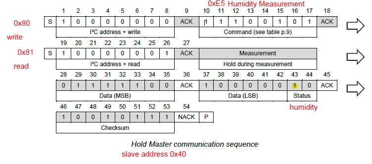
	I2caRegs.I2CDXR = 0xE5 ;						/*0x03 is '00000011',enable AEN and PON       */

	while(I2caRegs.I2CSTR.bit.SCD == 0);			// wait for STOP condition
	I2caRegs.I2CSTR.bit.SCD = 1; //clear stop condition flag

	InitPieCtrl();		// basic setup of PIE table; from DSP2833x_PieCtrl.c
	InitPieVectTable();	// default ISR's in PIE

	EALLOW;
	PieVectTable.TINT0 = &cpu_timer0_isr;
	EDIS;

	InitCpuTimers();	// basic setup CPU Timer0, 1 and 2
	ConfigCpuTimer(&CpuTimer0,150,100000);

	PieCtrlRegs.PIEIER1.bit.INTx7 = 1;

	IER |=1;

	EINT;
	ERTM;

	CpuTimer0Regs.TCR.bit.TSS = 0;	// start timer0

	//step 2 : start read the sensor data including 1 byte pointer register==>2 byte sensor data (upper 8bit) + (lower 8bit)
	while(1)
	{    
	  		while(CpuTimer0.InterruptCount == 0);
			CpuTimer0.InterruptCount = 0;

			EALLOW;
			SysCtrlRegs.WDKEY = 0x55;	// service WD #1
			EDIS;

			//	Send START and set pointer to temperature - register
			I2caRegs.I2CCNT 	= 1;				// pointer to temperature register, count 1 bit only
			I2caRegs.I2CDXR		= 0x81;// set Pointer Address to pointer_temperature

			// Send start as master transmitter
	 		I2caRegs.I2CMDR.all = 0x6620; //only change stop to '0', do not generate stop. all others are the same as 6E20
			/*	Bit15 = 0;	no NACK in receiver mode
				Bit14 = 1;  FREE on emulation halt
				Bit13 = 1;  STT  generate START 
				Bit12 = 0;	reserved
				Bit11 = 0;  STP  not generate STOP
				Bit10 = 1;  MST  master mode
				Bit9  = 1;  TRX  master - transmitter mode
				Bit8  = 0;	XA   7 bit address mode
				Bit7  = 0;  RM   nonrepeat mode, I2CCNT determines # of bytes
				Bit6  = 1;  DLB  no loopback mode ,it should be '0', corrected by alex.J
				Bit5  = 1;  IRS  I2C module enabled
				Bit4  = 0;  STB  no start byte mode
				Bit3  = 0;  FDF  no free data format
				Bit2-0: 0;  BC   8 bit per data byte,000	*/
			while(I2caRegs.I2CSTR.bit.ARDY == 0);			// 0=previous cycle has not completed, wait for access ready condition

			I2caRegs.I2CCNT		= 1;	// read 2 byte temperature
			I2caRegs.I2CMDR.all = 0x6C20; //only change bit9 to 0, means master-receiver mode
			/*	Bit15 = 0;	no NACK in receiver mode
				Bit14 = 1;  FREE on emulation halt
				Bit13 = 1;  STT  generate START 
				Bit12 = 0;	reserved
				Bit11 = 1;  STP  generate STOP
				Bit10 = 1;  MST  master mode
				Bit9  = 0;  TRX  master - receiver mode
				Bit8  = 0;	XA   7 bit address mode
				Bit7  = 0;  RM   nonrepeat mode, I2CCNT determines # of bytes
				Bit6  = 0;  DLB  no loopback mode
				Bit5  = 1;  IRS  I2C module enabled
				Bit4  = 0;  STB  no start byte mode
				Bit3  = 0;  FDF  no free data format
				Bit2-0: 0;  BC   8 bit per data byte	*/

			while(I2caRegs.I2CSTR.bit.RRDY == 0);	//0 means receive data NOT available in 12CDRR, wait for 1st byte
			clear_light_low = I2caRegs.I2CDRR;
						// read upper 8 Bit (integers)// read upper 8 Bit (integers)
			// RRDY is automatically cleared by read of I2CDRR 

	  		GpioDataRegs.GPBTOGGLE.bit.GPIO34 = 0;		// toggle red LED LD3 @ 28335CC
	}
} 

void Gpio_select(void)
{
	EALLOW;
	GpioCtrlRegs.GPAMUX1.all = 0;			// GPIO15 ... GPIO0 = General Puropse I/O
	GpioCtrlRegs.GPAMUX2.all = 0;			// GPIO31 ... GPIO16 = General Purpose I/O
	
	GpioCtrlRegs.GPBMUX1.all = 0;			// GPIO47 ... GPIO32 = General Purpose I/O
	GpioCtrlRegs.GPBMUX1.bit.GPIO32 = 1;	// GPIO32 = I2C - SDA
	GpioCtrlRegs.GPBMUX1.bit.GPIO33 = 1;	// GPIO33 = I2C - SCL

	GpioCtrlRegs.GPBPUD.bit.GPIO32 = 0;    // Enable pull-up for GPIO32 (SDAA)
	GpioCtrlRegs.GPBPUD.bit.GPIO33 = 0;	   // Enable pull-up for GPIO33 (SCLA)

	GpioCtrlRegs.GPBQSEL1.bit.GPIO32 = 3;  // Asynch input GPIO32 (SDAA)
    GpioCtrlRegs.GPBQSEL1.bit.GPIO33 = 3;  // Asynch input GPIO33 (SCLA)

	GpioCtrlRegs.GPBMUX2.all = 0;			// GPIO63 ... GPIO48 = General Purpose I/O

	GpioCtrlRegs.GPCMUX1.all = 0;			// GPIO79 ... GPIO64 = General Purpose I/O
	GpioCtrlRegs.GPCMUX2.all = 0;			// GPIO87 ... GPIO80 = General Purpose I/O
	 

	GpioCtrlRegs.GPADIR.all = 0;			// GPIO0 to 31 as inputs
	GpioCtrlRegs.GPADIR.bit.GPIO9 = 1;		// GPIO9 = LED LD1
	GpioCtrlRegs.GPADIR.bit.GPIO11 = 1;		// GpIO11 = LED LD2

	GpioCtrlRegs.GPBDIR.all = 0;			// GPIO63-32 as inputs
	GpioCtrlRegs.GPBDIR.bit.GPIO34 = 1;		// peripheral explorer: LED LD3 at GPIO34
	GpioCtrlRegs.GPBDIR.bit.GPIO49 = 1; 	// peripheral explorer: LED LD4 at GPIO49

	GpioCtrlRegs.GPCDIR.all = 0;			// GPIO87-64 as inputs
	EDIS;
}  

void I2CA_Init(void)
{
	
	I2caRegs.I2CMDR.bit.IRS = 0;	// Reset the I2C module
	// I2C slave address register
	I2caRegs.I2CSAR = TCS24725_SLAVE;
	// I2C Prescale Register
	I2caRegs.I2CPSC.all = 14;		// Internal I2C module clock = SYSCLK/(PSC +1)
								    // = 10 MHz
								    
    I2caRegs.I2CCLKL = 95;			// Tmaster = (PSC +1)[ICCL + 5 + ICCH + 5] / 150MHz
	I2caRegs.I2CCLKH = 95;			// Tmaster =  10 [ICCL + ICCH + 10] / 150 MHz
									// d = 5  for IPSC >1
									
									// for I2C 50 kHz:
									// Tmaster = 20 µs *150 MHz / 10 = 200 = (ICCL + ICCH +10)  
									// ICCL + ICCH = 190
									// ICCL = ICH = 190/2 = 95	

//	I2caRegs.I2CCLKL = 45;
//	I2caRegs.I2CCLKH = 45;			// for I2C 100 kHz:
									// Tmaster = 10 µs *150 MHz / 10 = 100 = (ICCL + ICCH + 10)  
									// ICCL + ICCH = 90
									// ICCL = ICH = 90/2 = 45 	

	I2caRegs.I2CMDR.bit.IRS = 1;	// Take I2C out of reset
}

interrupt void cpu_timer0_isr(void)
{
	CpuTimer0.InterruptCount++;
	EALLOW;
	SysCtrlRegs.WDKEY = 0xAA;	// service WD #2
	EDIS;
	PieCtrlRegs.PIEACK.all = PIEACK_GROUP1;
}
//===========================================================================
// End of SourceCode.
//===========================================================================

  • Alex,

    Have you checked SCL with an oscilloscope to make sure the line isn't held low by the slave?
  • hi Adam,

    Thanks so much for your reply!! you don't know how long have I waited for someone can help me a little bit :-(.

    I did use the oscilloscope to check the SCL and SDA pin signal when the code I pasted above is running.

    Both the SDA and SCK signal are maintained around 3.2V, so it should means they maintained at high voltage level. The pull-up resistor works fine.

    regards,

    alex

  • new updates

    hi Adam,

    Now i really doubts that is the example I use actually can't work at all?

    To verify where the problem comes from, i even bought another humidity sensor which I2C communication protocol is almost as same  as the TMP100 sensor shown in the example.

    The only change I do is to change the slave address from 0x48 to 0x40, write address from 1 to 0x80, write command register from 0x60 to 0xE5(read humidity value), read address from 0 to 0x81. 

    after that, i run the program again and still found out that the code is always paused at the either

    while(I2caRegs.I2CSTR.bit.XRDY == 0);

    or while(I2caRegs.I2CSTR.bit.SCD == 0);.

    i attached my code and the humidity sensor below.


    //
    //      Lab12_2: TMS320F28335
    //      (C) Frank Bormann
    //
    //###########################################################################
    //
    // FILE:	Lab12_2.c
    //
    // TITLE:	DSP28335 I2C test
    //          Temperature Sensor TMP100 connected to GPIO33 (SCL) and GPIO32(SDA)
    //			LED GPIO34 as life indicator 100 ms toggle
    //			12 bit mode of TMP100, 1/16 degree celcius resolution
    //			use watch window for variable "temperature" (type int; qvalue:8)
    //###########################################################################
    //
    //  Ver | dd mmm yyyy | Who  | Description of changes
    // =====|=============|======|===============================================
    //  3.0 | 24 Jul 2009 | F.B. | Lab12_1  F28335; Header-files Version 1.20 
    //  3.1 | 15 Nov 2009 | F.B  | Lab12_1 for F28335 @30MHz and PE revision 5
    //###########################################################################
    #include "DSP2833x_Device.h"
    
    // TMP100 commands
    #define TMP100_SLAVE 			0x40	// slave address TMP100 (ADDR0=ADDR1=0)
    #define POINTER_TEMPERATURE 	0x81
    #define POINTER_CONFIGURATION 	0x80
    #define POINTER_T_LOW 			2
    #define POINTER_T_HIGH 			3
    
    // external function prototypes
    extern void InitSysCtrl(void);
    extern void InitPieCtrl(void);
    extern void InitPieVectTable(void);
    extern void InitCpuTimers(void);
    extern void ConfigCpuTimer(struct CPUTIMER_VARS *, float, float);
    
    
    // Prototype statements for functions found within this file.
    void Gpio_select(void);
    void I2CA_Init(void);
    interrupt void cpu_timer0_isr(void);
    
    int temperature;	// temperature = 2' Komplement of temparature (-128 ... +127 Celsius)
    					// is an I8Q8 - Value 
    //###########################################################################
    //						main code									
    //###########################################################################
    void main(void)
    {
    	InitSysCtrl();		// Basic Core Init from DSP2833x_SysCtrl.c
    
    	EALLOW;
       	SysCtrlRegs.WDCR= 0x00AF;	// Re-enable the watchdog 
       	EDIS;			// 0x00AF  to NOT disable the Watchdog, Prescaler = 64
    
    	DINT;			// Disable all interrupts
    	
    	Gpio_select();	// GPIO9, GPIO11, GPIO34 and GPIO49 as output
    					// to 4 LEDs at Peripheral Explorer	
    
    	//	Initialize I2C
    	I2CA_Init();
    
    	// Send START, set pointer to Configuration register and set resolution to 12 bit
    	I2caRegs.I2CCNT = 2;	
    	I2caRegs.I2CDXR = POINTER_CONFIGURATION;
    	I2caRegs.I2CMDR.all = 0x6E20;
    	/*	Bit15 = 0;	no NACK in receiver mode
    		Bit14 = 1;  FREE on emulation halt
    		Bit13 = 1;  STT  generate START 
    		Bit12 = 0;	reserved
    		Bit11 = 1;  STP  generate STOP
    		Bit10 = 1;  MST  master mode
    		Bit9  = 1;  TRX  master - transmitter mode
    		Bit8  = 0;	XA   7 bit address mode
    		Bit7  = 0;  RM   nonrepeat mode, I2CCNT determines # of bytes
    		Bit6  = 1;  DLB  no loopback mode
    		Bit5  = 1;  IRS  I2C module enabled
    		Bit4  = 0;  STB  no start byte mode
    		Bit3  = 0;  FDF  no free data format
    		Bit2-0: 0;  BC   8 bit per data byte	*/
    	while(I2caRegs.I2CSTR.bit.XRDY == 0);		// wait until first byte is out
    	I2caRegs.I2CDXR = 0xE5;						// TMP100 in 12 bit mode (R1=R0=1)
    	while(I2caRegs.I2CSTR.bit.SCD == 0);			// wait for STOP condition
    	I2caRegs.I2CSTR.bit.SCD = 1;
    
    	InitPieCtrl();		// basic setup of PIE table; from DSP2833x_PieCtrl.c
    	InitPieVectTable();	// default ISR's in PIE
    
    	EALLOW;
    	PieVectTable.TINT0 = &cpu_timer0_isr;
    	EDIS;
    
    	InitCpuTimers();	// basic setup CPU Timer0, 1 and 2
    	ConfigCpuTimer(&CpuTimer0,150,100000);
    
    	PieCtrlRegs.PIEIER1.bit.INTx7 = 1;
    
    	IER |=1;
    
    	EINT;
    	ERTM;
    
    	CpuTimer0Regs.TCR.bit.TSS = 0;	// start timer0
    
    	while(1)
    	{    
    	  		while(CpuTimer0.InterruptCount == 0);
    			CpuTimer0.InterruptCount = 0;
    
    			EALLOW;
    			SysCtrlRegs.WDKEY = 0x55;	// service WD #1
    			EDIS;
    
    			//	Send START and set pointer to temperature - register
    			I2caRegs.I2CCNT 	= 1;				// pointer to temperature register
    			I2caRegs.I2CDXR		= POINTER_TEMPERATURE;
    			// Send start as master transmitter
    	 		I2caRegs.I2CMDR.all = 0x6620;
    			/*	Bit15 = 0;	no NACK in receiver mode
    				Bit14 = 1;  FREE on emulation halt
    				Bit13 = 1;  STT  generate START 
    				Bit12 = 0;	reserved
    				Bit11 = 0;  STP  not generate STOP
    				Bit10 = 1;  MST  master mode
    				Bit9  = 1;  TRX  master - transmitter mode
    				Bit8  = 0;	XA   7 bit address mode
    				Bit7  = 0;  RM   nonrepeat mode, I2CCNT determines # of bytes
    				Bit6  = 1;  DLB  no loopback mode
    				Bit5  = 1;  IRS  I2C module enabled
    				Bit4  = 0;  STB  no start byte mode
    				Bit3  = 0;  FDF  no free data format
    				Bit2-0: 0;  BC   8 bit per data byte	*/
    			while(I2caRegs.I2CSTR.bit.ARDY == 0);			// wait for access ready condition
    
    			I2caRegs.I2CCNT		= 2;	// read 2 byte temperature 
    			I2caRegs.I2CMDR.all = 0x6C20;
    			/*	Bit15 = 0;	no NACK in receiver mode
    				Bit14 = 1;  FREE on emulation halt
    				Bit13 = 1;  STT  generate START 
    				Bit12 = 0;	reserved
    				Bit11 = 1;  STP  generate STOP
    				Bit10 = 1;  MST  master mode
    				Bit9  = 0;  TRX  master - receiver mode
    				Bit8  = 0;	XA   7 bit address mode
    				Bit7  = 0;  RM   nonrepeat mode, I2CCNT determines # of bytes
    				Bit6  = 0;  DLB  no loopback mode
    				Bit5  = 1;  IRS  I2C module enabled
    				Bit4  = 0;  STB  no start byte mode
    				Bit3  = 0;  FDF  no free data format
    				Bit2-0: 0;  BC   8 bit per data byte	*/
    
    			while(I2caRegs.I2CSTR.bit.RRDY == 0);	// wait for 1st byte
    			temperature = I2caRegs.I2CDRR << 8;			// read upper 8 Bit (integers)
    			// RRDY is automatically cleared by read of I2CDRR 
    			while(I2caRegs.I2CSTR.bit.RRDY == 0);	// wait for 2nd byte
    			temperature += I2caRegs.I2CDRR;				// read lower 8 Bit (fractions)
    
    	  		GpioDataRegs.GPBTOGGLE.bit.GPIO34 = 1;		// toggle red LED LD3 @ 28335CC
    	}
    } 
    
    void Gpio_select(void)
    {
    	EALLOW;
    	GpioCtrlRegs.GPAMUX1.all = 0;			// GPIO15 ... GPIO0 = General Puropse I/O
    	GpioCtrlRegs.GPAMUX2.all = 0;			// GPIO31 ... GPIO16 = General Purpose I/O
    	
    	GpioCtrlRegs.GPBMUX1.all = 0;			// GPIO47 ... GPIO32 = General Purpose I/O
    	GpioCtrlRegs.GPBMUX1.bit.GPIO32 = 1;	// GPIO32 = I2C - SDA
    	GpioCtrlRegs.GPBMUX1.bit.GPIO33 = 1;	// GPIO33 = I2C - SCL
    
    	GpioCtrlRegs.GPBPUD.bit.GPIO32 = 0;    // Enable pull-up for GPIO32 (SDAA)
    	GpioCtrlRegs.GPBPUD.bit.GPIO33 = 0;	   // Enable pull-up for GPIO33 (SCLA)
    
    	GpioCtrlRegs.GPBQSEL1.bit.GPIO32 = 3;  // Asynch input GPIO32 (SDAA)
        GpioCtrlRegs.GPBQSEL1.bit.GPIO33 = 3;  // Asynch input GPIO33 (SCLA)
    
    	GpioCtrlRegs.GPBMUX2.all = 0;			// GPIO63 ... GPIO48 = General Purpose I/O
    
    	GpioCtrlRegs.GPCMUX1.all = 0;			// GPIO79 ... GPIO64 = General Purpose I/O
    	GpioCtrlRegs.GPCMUX2.all = 0;			// GPIO87 ... GPIO80 = General Purpose I/O
    	 
    
    	GpioCtrlRegs.GPADIR.all = 0;			// GPIO0 to 31 as inputs
    	GpioCtrlRegs.GPADIR.bit.GPIO9 = 1;		// GPIO9 = LED LD1
    	GpioCtrlRegs.GPADIR.bit.GPIO11 = 1;		// GpIO11 = LED LD2
    
    	GpioCtrlRegs.GPBDIR.all = 0;			// GPIO63-32 as inputs
    	GpioCtrlRegs.GPBDIR.bit.GPIO34 = 1;		// peripheral explorer: LED LD3 at GPIO34
    	GpioCtrlRegs.GPBDIR.bit.GPIO49 = 1; 	// peripheral explorer: LED LD4 at GPIO49
    
    	GpioCtrlRegs.GPCDIR.all = 0;			// GPIO87-64 as inputs
    	EDIS;
    }  
    
    void I2CA_Init(void)
    {
    	
    	I2caRegs.I2CMDR.bit.IRS = 0;	// Reset the I2C module
    	// I2C slave address register
    	I2caRegs.I2CSAR = TMP100_SLAVE;	
    	// I2C Prescale Register
    	I2caRegs.I2CPSC.all = 14;		// Internal I2C module clock = SYSCLK/(PSC +1)
    								    // = 10 MHz
    								    
    	I2caRegs.I2CCLKL = 95;			// Tmaster = (PSC +1)[ICCL + 5 + ICCH + 5] / 150MHz
    	I2caRegs.I2CCLKH = 95;			// Tmaster =  10 [ICCL + ICCH + 10] / 150 MHz 
    									// d = 5  for IPSC >1
    									
    									// for I2C 50 kHz:
    									// Tmaster = 20 �s *150 MHz / 10 = 200 = (ICCL + ICCH +10)  
    									// ICCL + ICCH = 190
    									// ICCL = ICH = 190/2 = 95	
    
    //	I2caRegs.I2CCLKL = 45;			
    //	I2caRegs.I2CCLKH = 45;			// for I2C 100 kHz:
    									// Tmaster = 10 �s *150 MHz / 10 = 100 = (ICCL + ICCH + 10)  
    									// ICCL + ICCH = 90
    									// ICCL = ICH = 90/2 = 45 	
    
    	I2caRegs.I2CMDR.bit.IRS = 1;	// Take I2C out of reset
    }
    
    interrupt void cpu_timer0_isr(void)
    {
    	CpuTimer0.InterruptCount++;
    	EALLOW;
    	SysCtrlRegs.WDKEY = 0xAA;	// service WD #2
    	EDIS;
    	PieCtrlRegs.PIEACK.all = PIEACK_GROUP1;
    }
    //===========================================================================
    // End of SourceCode.
    //===========================================================================
    

    1899_HTU21D_chip_datasheet.pdf

  • hi Adam,

    sorry that maybe i didnt' answer your question clearly.

    both SCL and SDA line 's signal are at HIGH voltage level around 3.2V before the program started.

    After started, when the program runs at the line either'while(I2caRegs.I2CSTR.bit.XRDY == 0); ' or ' while(I2caRegs.I2CSTR.bit.XRDY == 0);'
    YOU ARE RIGHT, the SCL line is at LOW voltage level!

    what caused the MCU keep waiting for the 'STOP' condition?

    regards,
    alex

    thanks
  • Alex,

    You can look at the oscilloscope to see how much of the transfer has completed. Please post a screenshot if you want me to look at it. It's hard to tell what's going on without context.

    SCL can be held low by the slave to delay the transfer. It can be held low by the master if it's waiting for more data to send.

  • hi adam, here is the screencapture i got from the oscilloscope when the code paused at the line 

    while(I2caRegs.I2CSTR.bit.SCD == 0); // wait for STOP condition

    The CH1 stands for SCL and CH2 stands for SDA. it seems the MCU keeps waiting for the stop condition :-(.

    Then I changed the while(I2caRegs.I2CSTR.bit.SCD == 0) to while(I2caRegs.I2CSTR.bit.NACK== 0)

    (i know it is wrong, but i just take a try to know what will happen).

    and see the signal in the oscilloscope like this


    The CH1 (SCL) is still always held at low.

    regards,

    alex

  • Sorry, I meant a screenshot showing the whole transfer, beginning with the start condition.
  • just uploaded two screencapture, pls take a look.

    click the wrong button before when i am not finished writing the post. sorry about that :-(
  • hi Adam,

    And also I attached the I2C communication sequence from the sensor datasheet that I use.

    from the sequence it seems there is only need one 'stop' needed at the end of the whole sequence. So is it means that I need to set the I2caRegs.I2CMDR.all = 0x6620 instead of 0x6E20 ?

    but in the example , they use 0x6E20.

    regards,

    alex

  • Alex,

    I think the code is incorrect. It's trying to write the address byte using I2CDXR, which is wrong. The address byte is set by I2CSAR and the I2CMDR.TRX bit. If you want to write 0x80 for the address byte, set I2CSAR to 0x40 and I2CMDR.TRX to 0.

    If you remove the lines where POINTER_CONFIGURATION or POINTER_TEMPERATURE is written to I2CDXR, you might get to the while loop.

    You can also try using command 0xF5 instead of 0xE5 to prevent the sensor from holding SCL low. With command 0xF5, the sensor will NACK if it has no data to send.
  • hi Adam,

    Thanks for your quick reply! 

    Sorry that I roughly understand what you mean, but still not clear about how to write the pointer address(0x80 for write).

    for example, right now I need to write command 0xF5 (as you suggested, for the humidity measurement command) to the pointer address (0x80), you suggested to set SAR as 0x40 (which is the device slave address), and set I2CMDR.TRX=0, which means setting the MCU as the master -receiver mode right? 

    but how can i sent 0xF5 to the pointer address 0x80?

    anyway, i guess you mean to modify the code like this:

    	I2caRegs.I2CCNT = 2;	// means the DXR includes 2 byte including POINTER_CONFIGURATION and 0x60 for data bit setting
    	// I2caRegs.I2CDXR = Write_address;// address for writing
    
    	I2caRegs.I2CMDR.all = 0x6C20; 
    	
    	while(I2caRegs.I2CSTR.bit.XRDY == 0);		// wait until first byte is out
    
    	I2caRegs.I2CDXR = Write_humidity_unhold ;   /*0xF5 read humidity       */
    
       while(I2caRegs.I2CSTR.bit.SCD == 0);			// wait for STOP condition
    		
    	I2caRegs.I2CSTR.bit.SCD = 1; //clear stop condition flag

    and also, i just tidy up my whole code and pasted below to let you check.

    // TITLE:	DSP28335 I2C test
    //          temperature and humidity sensor HTU21D
    //          slave address 0x40
    //          I2C communication structure: send write register address (0x80) + command 0xF5 (for humidity measurement)
    //          and then sent read register address (0x81)
    //###########################################################################
    //
    //  Ver | dd mmm yyyy | Who  | Description of changes
    // =====|=============|======|===============================================
    //  3.0 | 24 Jul 2009 | F.B. | Lab12_1  F28335; Header-files Version 1.20 
    //  3.1 | 15 Nov 2009 | F.B  | Lab12_1 for F28335 @30MHz and PE revision 5
    //###########################################################################
    #include "DSP2833x_Device.h"
    
    #define SLAVE_Address 			    0x40	
    
    
    #define Write_address               0x80
    #define Read_address                0x81
    #define Write_humidity_hold         0xE5
    #define Write_humidity_unhold       0xF5
    #define Write_temperature_unhold    0xF3
    
    
    // external function prototypes
    extern void InitSysCtrl(void);
    extern void InitPieCtrl(void);
    extern void InitPieVectTable(void);
    extern void InitCpuTimers(void);
    extern void ConfigCpuTimer(struct CPUTIMER_VARS *, float, float);
    
    
    // Prototype statements for functions found within this file.
    void Gpio_select(void);
    void I2CA_Init(void);
    interrupt void cpu_timer0_isr(void);
    
    int Value_Read;
    
    //###########################################################################
    //						main code									
    //###########################################################################
    void main(void)
    {
    	InitSysCtrl();		// Basic Core Init from DSP2833x_SysCtrl.c
    
    	EALLOW;
       	SysCtrlRegs.WDCR= 0x00AF;	// Re-enable the watchdog 
       	EDIS;			// 0x00AF  to NOT disable the Watchdog, Prescaler = 64
    
    	DINT;			// Disable all interrupts
    	
    	Gpio_select();	// GPI031-LED2, GPIO34-LED3 as output
    					// to 2 LEDs on F28335 control-card
    
    	I2CA_Init(); 	//	Initialize I2C device slave address is issued in I2CA_Init() 0x29
    
    	// step 1 : do the configuration:
    	//----------------------------------------------------//
    	// Send START, set pointer to Configuration register and set resolution to 12 bit
    	//hence it is master-transmitter mode to write register to the sensor
    
    	//step 1.1 set integration time to address 0x01+0xFF (2.4ms)
    
    	//step 1.2 set gain to address 0x0F + 0x00 (1*gain)
    
    	//step 1.3 Enable Device to address 0x00+0x03
    
    
    	I2caRegs.I2CCNT = 1;	// means the DXR includes 2 byte including POINTER_CONFIGURATION and 0x60 for data bit setting
    	//I2caRegs.I2CDXR = Write_address;// address for writing
    
    	I2caRegs.I2CMDR.all = 0x6C20; //0x6E20 convert to binary is 0110111000100000
    	/*	            Bit15 = 0;	no NACK in receiver mode
    					Bit14 = 1;  FREE on emulation halt
    					Bit13 = 1;  STT  generate START
    					Bit12 = 0;	reserved
    					Bit11 = 0;  STP  not generate STOP
    					Bit10 = 1;  MST  master mode
    					Bit9  = 1;  TRX  master - transmitter mode
    					Bit8  = 0;	XA   7 bit address mode
    					Bit7  = 0;  RM   nonrepeat mode, I2CCNT determines # of bytes
    					Bit6  = 1;  DLB  no loopback mode ,it should be '0', corrected by alex.J
    					Bit5  = 1;  IRS  I2C module enabled
    					Bit4  = 0;  STB  no start byte mode
    					Bit3  = 0;  FDF  no free data format
    					Bit2-0: 0;  BC   8 bit per data byte,000	*/
    
    	while(I2caRegs.I2CSTR.bit.XRDY == 0);		// wait until first byte is out
    
    	I2caRegs.I2CDXR = Write_humidity_unhold ;   /*0xF5 read humidity       */
    
       while(I2caRegs.I2CSTR.bit.SCD == 0);			// wait for STOP condition
    		
    	I2caRegs.I2CSTR.bit.SCD = 1; //clear stop condition flag
    
    	InitPieCtrl();		// basic setup of PIE table; from DSP2833x_PieCtrl.c
    	InitPieVectTable();	// default ISR's in PIE
    
    	EALLOW;
    	PieVectTable.TINT0 = &cpu_timer0_isr;
    	EDIS;
    
    	InitCpuTimers();	// basic setup CPU Timer0, 1 and 2
    	ConfigCpuTimer(&CpuTimer0,150,100000);
    
    	PieCtrlRegs.PIEIER1.bit.INTx7 = 1;
    
    	IER |=1;
    
    	EINT;
    	ERTM;
    
    	CpuTimer0Regs.TCR.bit.TSS = 0;	// start timer0
    
    	//step 2 : start read the sensor data including 1 byte pointer register==>2 byte sensor data (upper 8bit) + (lower 8bit)
    	while(1)
    	{    
    
    		    while(CpuTimer0.InterruptCount == 0);
    
    		    CpuTimer0.InterruptCount = 0;
    
    			EALLOW;
    			SysCtrlRegs.WDKEY = 0x55;	// service WD #1
    			EDIS;
    
    			//	Send START and set pointer to temperature - register
    			I2caRegs.I2CCNT 	= 1;				// pointer to temperature register, count 1 bit only
    			I2caRegs.I2CDXR		= Read_address;// address for reading
    
    			// Send start as master transmitter
    	 		I2caRegs.I2CMDR.all = 0x6620; //only change stop to '0', do not generate stop. all others are the same as 6E20
    			/*	Bit15 = 0;	no NACK in receiver mode
    				Bit14 = 1;  FREE on emulation halt
    				Bit13 = 1;  STT  generate START 
    				Bit12 = 0;	reserved
    				Bit11 = 0;  STP  not generate STOP
    				Bit10 = 1;  MST  master mode
    				Bit9  = 1;  TRX  master - transmitter mode
    				Bit8  = 0;	XA   7 bit address mode
    				Bit7  = 0;  RM   nonrepeat mode, I2CCNT determines # of bytes
    				Bit6  = 1;  DLB  no loopback mode ,it should be '0', corrected by alex.J
    				Bit5  = 1;  IRS  I2C module enabled
    				Bit4  = 0;  STB  no start byte mode
    				Bit3  = 0;  FDF  no free data format
    				Bit2-0: 0;  BC   8 bit per data byte,000	*/
    			while(I2caRegs.I2CSTR.bit.ARDY == 0);			// 0=previous cycle has not completed, wait for access ready condition
    
    			I2caRegs.I2CCNT		= 2;	// read 2 byte temperature
    			I2caRegs.I2CMDR.all = 0x6C20; //only change bit9 to 0, means master-receiver mode
    			/*	Bit15 = 0;	no NACK in receiver mode
    				Bit14 = 1;  FREE on emulation halt
    				Bit13 = 1;  STT  generate START 
    				Bit12 = 0;	reserved
    				Bit11 = 1;  STP  generate STOP
    				Bit10 = 1;  MST  master mode
    				Bit9  = 0;  TRX  master - receiver mode
    				Bit8  = 0;	XA   7 bit address mode
    				Bit7  = 0;  RM   nonrepeat mode, I2CCNT determines # of bytes
    				Bit6  = 0;  DLB  no loopback mode
    				Bit5  = 1;  IRS  I2C module enabled
    				Bit4  = 0;  STB  no start byte mode
    				Bit3  = 0;  FDF  no free data format
    				Bit2-0: 0;  BC   8 bit per data byte	*/
    
    			while(I2caRegs.I2CSTR.bit.RRDY == 1);	//0 means receive data NOT available in 12CDRR, wait for 1st byte
    			Value_Read = I2caRegs.I2CDRR << 8; // read upper 8 Bit (integers)
    			Value_Read += I2caRegs.I2CDRR;// RRDY is automatically cleared by read of I2CDRR 
    
    	  		GpioDataRegs.GPBTOGGLE.bit.GPIO34 = 1;		// toggle red LED LD3 @ 28335CC
    	  		GpioDataRegs.GPATOGGLE.bit.GPIO31 = 1;
    	}
    } 
    
    void Gpio_select(void)
    {
    	EALLOW;
    	GpioCtrlRegs.GPAMUX1.all = 0;			// GPIO15 ... GPIO0 = General Puropse I/O
    	GpioCtrlRegs.GPAMUX2.all = 0;			// GPIO31 ... GPIO16 = General Purpose I/O
    	
    	GpioCtrlRegs.GPBMUX1.all = 0;			// GPIO47 ... GPIO32 = General Purpose I/O
    	GpioCtrlRegs.GPBMUX1.bit.GPIO32 = 1;	// GPIO32 = I2C - SDA
    	GpioCtrlRegs.GPBMUX1.bit.GPIO33 = 1;	// GPIO33 = I2C - SCL
    
    	GpioCtrlRegs.GPBPUD.bit.GPIO32 = 0;    // Enable pull-up for GPIO32 (SDAA)
    	GpioCtrlRegs.GPBPUD.bit.GPIO33 = 0;	   // Enable pull-up for GPIO33 (SCLA)
    
    	GpioCtrlRegs.GPBQSEL1.bit.GPIO32 = 3;  // Asynch input GPIO32 (SDAA)
        GpioCtrlRegs.GPBQSEL1.bit.GPIO33 = 3;  // Asynch input GPIO33 (SCLA)
    
    	GpioCtrlRegs.GPBMUX2.all = 0;			// GPIO63 ... GPIO48 = General Purpose I/O
    
    	GpioCtrlRegs.GPCMUX1.all = 0;			// GPIO79 ... GPIO64 = General Purpose I/O
    	GpioCtrlRegs.GPCMUX2.all = 0;			// GPIO87 ... GPIO80 = General Purpose I/O
    	 
    
    	GpioCtrlRegs.GPADIR.all = 0;			// GPIO0 to 31 as inputs
    //	GpioCtrlRegs.GPADIR.bit.GPIO9 = 1;		// GPIO9 = LED LD1
    	GpioCtrlRegs.GPADIR.bit.GPIO31 = 1;		// GpIO11 = LED LD2
    
    	GpioCtrlRegs.GPBDIR.all = 0;			// GPIO63-32 as inputs
    	GpioCtrlRegs.GPBDIR.bit.GPIO34 = 1;		// peripheral explorer: LED LD3 at GPIO34
    	//GpioCtrlRegs.GPBDIR.bit.GPIO49 = 1; 	// peripheral explorer: LED LD4 at GPIO49
    
    	GpioCtrlRegs.GPCDIR.all = 0;			// GPIO87-64 as inputs
    	EDIS;
    }  
    
    void I2CA_Init(void)
    {
    	
    	I2caRegs.I2CMDR.bit.IRS = 0;	// Reset the I2C module
    	// I2C slave address register
    	I2caRegs.I2CSAR = SLAVE_Address;
    	// I2C Prescale Register
    	I2caRegs.I2CPSC.all = 14;		// Internal I2C module clock = SYSCLK/(PSC +1)
    								    // = 10 MHz
    								    
        I2caRegs.I2CCLKL = 95;			// Tmaster = (PSC +1)[ICCL + 5 + ICCH + 5] / 150MHz
    	I2caRegs.I2CCLKH = 95;			// Tmaster =  10 [ICCL + ICCH + 10] / 150 MHz
    									// d = 5  for IPSC >1
    									
    									// for I2C 50 kHz:
    									// Tmaster = 20 �s *150 MHz / 10 = 200 = (ICCL + ICCH +10)  
    									// ICCL + ICCH = 190
    									// ICCL = ICH = 190/2 = 95	
    
    //	I2caRegs.I2CCLKL = 45;
    //	I2caRegs.I2CCLKH = 45;			// for I2C 100 kHz:
    									// Tmaster = 10 �s *150 MHz / 10 = 100 = (ICCL + ICCH + 10)  
    									// ICCL + ICCH = 90
    									// ICCL = ICH = 90/2 = 45 	
    
    	I2caRegs.I2CMDR.bit.IRS = 1;	// Take I2C out of reset
    }
    
    interrupt void cpu_timer0_isr(void)
    {
    	CpuTimer0.InterruptCount++;
    	EALLOW;
    	SysCtrlRegs.WDKEY = 0xAA;	// service WD #2
    	EDIS;
    	PieCtrlRegs.PIEACK.all = PIEACK_GROUP1;
    }
    //===========================================================================
    // End of SourceCode.
    //===========================================================================
    

  • Alex,

    The comments in the source code are misleading. According to the datasheet, the "pointer address" is really the device slave address. It's common to combine the 7-bit slave address and 1-bit read/write bit into a single 8-bit value since that's what gets sent on the bus. You can see this in the diagram on page 13 of the datasheet. Look for "I2C address + write" and "I2C address + read". That's what the 0x80 and 0x81 are.

    The I2C module sends the address automatically when the transfer starts. So you only have to send one data byte -- the command.

    The C file has "adafruit" in the title. This code might have been written to use an I2C multiplexer like this one:

    learn.adafruit.com/.../overview

    With a multiplexer, you need to send an extra data byte for the slave address.
  • By the way, where did you get the source code from? I couldn't find it in controlSUITE.
  • HI Adam,

    The I2C example I downloaded is from C2000 Teaching Materials, link:

    in the Lab12, they introduced the i2c communication coding example for reading data from a temperature sensor.

    regards,

    alex

  • hi adam,

    the C file titled with 'adafruit' because the sensor i use is bought from adafruit, which provide the breakout board for the sensor chip . sorry to make you misunderstand.

    As for your suggestion, I modified the coding based on your suggestion, but it doesn't work at all. 

    As you said, i write 0x40+write bit '0' and humidity command '0xE5' ,

    I2caRegs.I2CCNT = 1; //
    
    settingI2caRegs.I2CMDR.all = 0x6420; //NOT sure if this line is correct?
    
    /* Bit15 = 0; no NACK in receiver mode
    Bit14 = 1; FREE on emulation halt
    Bit13 = 1; STT generate START
    Bit12 = 0; reserved
    Bit11 = 0; STP NO generate STOP
    Bit10 = 1; MST master mode
    Bit9 = 0; TRX master - RECEIVE mode//as you suggested, TRX is 0 for write. but actually the I2C datasheet said 0 means receiver                                                                         //mode. i am confused about this,
    Bit8 = 0; XA 7 bit address mode
    Bit7 = 0; RM nonrepeat mode, I2CCNT determines # of bytes
    Bit6 = 0; DLB no loopback mode ,it should be '0', corrected by alex.J
    Bit5 = 1; IRS I2C module enabled
    Bit4 = 0; STB no start byte mode
    Bit3 = 0; FDF no free data format
    Bit2-0: 0; BC 8 bit per data byte,000 */
    
    while(I2caRegs.I2CSTR.bit.XRDY == 0); // wait until first byte is out
    
    I2caRegs.I2CDXR = Write_humidity_unhold ; /*0xF5 read humidity */
    
    // while(I2caRegs.I2CSTR.bit.SCD == 0); // wait for STOP condition
    
    //I2caRegs.I2CSTR.bit.SCD = 1; //clear stop condition flag
    

  • as for reading, it is 0x40 plus bit of '1' and then read 2 byte of humidity data

    i guess this coding is what you mean

    	I2caRegs.I2CCNT		= 2;	// read 2 byte temperature
    			I2caRegs.I2CMDR.all = 0x6620; //only change stop to '0', do not generate stop. all others are the same as 6E20
    					/*	Bit15 = 0;	no NACK in receiver mode
    						Bit14 = 1;  FREE on emulation halt
    						Bit13 = 1;  STT  generate START
    						Bit12 = 0;	reserved
    						Bit11 = 0;  STP  not generate STOP
    						Bit10 = 1;  MST  master mode
    						Bit9  = 1;  TRX  master - transmitter mode
    						Bit8  = 0;	XA   7 bit address mode
    						Bit7  = 0;  RM   nonrepeat mode, I2CCNT determines # of bytes
    						Bit6  = 1;  DLB  no loopback mode ,it should be '0', corrected by alex.J
    						Bit5  = 1;  IRS  I2C module enabled
    						Bit4  = 0;  STB  no start byte mode
    						Bit3  = 0;  FDF  no free data format
    						Bit2-0: 0;  BC   8 bit per data byte,000	*/
    
    			while(I2caRegs.I2CSTR.bit.RRDY == 1);	//0 means receive data NOT available in 12CDRR, wait for 1st byte
    			Value_Read = I2caRegs.I2CDRR << 8; // read upper 8 Bit (integers)
    			Value_Read += I2caRegs.I2CDRR;// RRDY is automatically cleared by read of I2CDRR 

    after I run this, it didn't shows the SCL is at low voltage level and SDA is at high voltage level always.which doesn't work at all.

    appreciated so much again for your help.

    here is the code file 

    // TITLE:	DSP28335 I2C test
    //          temperature and humidity sensor HTU21D
    //          slave address 0x40
    //          I2C communication structure: send write register address (0x80) + command 0xF5 (for humidity measurement)
    //          and then sent read register address (0x81)
    //###########################################################################
    //
    //  Ver | dd mmm yyyy | Who  | Description of changes
    // =====|=============|======|===============================================
    //  3.0 | 24 Jul 2009 | F.B. | Lab12_1  F28335; Header-files Version 1.20 
    //  3.1 | 15 Nov 2009 | F.B  | Lab12_1 for F28335 @30MHz and PE revision 5
    //###########################################################################
    #include "DSP2833x_Device.h"
    
    #define SLAVE_Address 			    0x40	
    
    
    #define Write_address               0x80
    #define Read_address                0x81
    #define Write_humidity_hold         0xE5
    #define Write_humidity_unhold       0xF5
    #define Write_temperature_unhold    0xF3
    
    
    // external function prototypes
    extern void InitSysCtrl(void);
    extern void InitPieCtrl(void);
    extern void InitPieVectTable(void);
    extern void InitCpuTimers(void);
    extern void ConfigCpuTimer(struct CPUTIMER_VARS *, float, float);
    
    
    // Prototype statements for functions found within this file.
    void Gpio_select(void);
    void I2CA_Init(void);
    interrupt void cpu_timer0_isr(void);
    
    int Value_Read;
    
    //###########################################################################
    //						main code									
    //###########################################################################
    void main(void)
    {
    	InitSysCtrl();		// Basic Core Init from DSP2833x_SysCtrl.c
    
    	EALLOW;
       	SysCtrlRegs.WDCR= 0x00AF;	// Re-enable the watchdog 
       	EDIS;			// 0x00AF  to NOT disable the Watchdog, Prescaler = 64
    
    	DINT;			// Disable all interrupts
    	
    	Gpio_select();	// GPI031-LED2, GPIO34-LED3 as output
    					// to 2 LEDs on F28335 control-card
    
    	I2CA_Init(); 	//	Initialize I2C device slave address is issued in I2CA_Init() 0x29
    
    	// step 1 : do the configuration:
    	//----------------------------------------------------//
    	// Send START, set pointer to Configuration register and set resolution to 12 bit
    	//hence it is master-transmitter mode to write register to the sensor
    
    	//step 1.1 set integration time to address 0x01+0xFF (2.4ms)
    
    	//step 1.2 set gain to address 0x0F + 0x00 (1*gain)
    
    	//step 1.3 Enable Device to address 0x00+0x03
    
    
    	I2caRegs.I2CCNT = 1;	// means the DXR includes 2 byte including POINTER_CONFIGURATION and 0x60 for data bit setting
    	//I2caRegs.I2CDXR = Write_address;// address for writing
    
    	I2caRegs.I2CMDR.all = 0x6420; //0x6C20 convert to binary is 0110110000100000
    	/*	            Bit15 = 0;	no NACK in receiver mode
    					Bit14 = 1;  FREE on emulation halt
    					Bit13 = 1;  STT  generate START
    					Bit12 = 0;	reserved
    					Bit11 = 0;  STP NO  generate STOP
    					Bit10 = 1;  MST  master mode
    					Bit9  = 0;  TRX  master - RECEIVE mode
    					Bit8  = 0;	XA   7 bit address mode
    					Bit7  = 0;  RM   nonrepeat mode, I2CCNT determines # of bytes
    					Bit6  = 0;  DLB  no loopback mode ,it should be '0', corrected by alex.J
    					Bit5  = 1;  IRS  I2C module enabled
    					Bit4  = 0;  STB  no start byte mode
    					Bit3  = 0;  FDF  no free data format
    					Bit2-0: 0;  BC   8 bit per data byte,000	*/
    
    	//while(I2caRegs.I2CSTR.bit.XRDY == 0);		// wait until first byte is out
    
    	I2caRegs.I2CDXR = Write_humidity_unhold ;   /*0xF5 read humidity       */
    
       while(I2caRegs.I2CSTR.bit.NACK == 0);			// wait for STOP condition
    		
    	//I2caRegs.I2CSTR.bit.SCD = 1; //clear stop condition flag
    
    	InitPieCtrl();		// basic setup of PIE table; from DSP2833x_PieCtrl.c
    	InitPieVectTable();	// default ISR's in PIE
    
    	EALLOW;
    	PieVectTable.TINT0 = &cpu_timer0_isr;
    	EDIS;
    
    	InitCpuTimers();	// basic setup CPU Timer0, 1 and 2
    	ConfigCpuTimer(&CpuTimer0,150,100000);
    
    	PieCtrlRegs.PIEIER1.bit.INTx7 = 1;
    
    	IER |=1;
    
    	EINT;
    	ERTM;
    
    	CpuTimer0Regs.TCR.bit.TSS = 0;	// start timer0
    
    	//step 2 : start read the sensor data including 1 byte pointer register==>2 byte sensor data (upper 8bit) + (lower 8bit)
    	while(1)
    	{    
    
    		    while(CpuTimer0.InterruptCount == 0);
    
    		    CpuTimer0.InterruptCount = 0;
    
    			EALLOW;
    			SysCtrlRegs.WDKEY = 0x55;	// service WD #1
    			EDIS;
    
    			//	Send START and set pointer to temperature - register
    		//	I2caRegs.I2CCNT 	= 1;				// pointer to temperature register, count 1 bit only
    			//I2caRegs.I2CDXR		= Read_address;// address for reading
    
    			// Send start as master transmitter
    
    			I2caRegs.I2CCNT		= 2;	// read 2 byte temperature
    			I2caRegs.I2CMDR.all = 0x6620; //only change stop to '0', do not generate stop. all others are the same as 6E20
    					/*	Bit15 = 0;	no NACK in receiver mode
    						Bit14 = 1;  FREE on emulation halt
    						Bit13 = 1;  STT  generate START
    						Bit12 = 0;	reserved
    						Bit11 = 0;  STP  not generate STOP
    						Bit10 = 1;  MST  master mode
    						Bit9  = 1;  TRX  master - transmitter mode
    						Bit8  = 0;	XA   7 bit address mode
    						Bit7  = 0;  RM   nonrepeat mode, I2CCNT determines # of bytes
    						Bit6  = 1;  DLB  no loopback mode ,it should be '0', corrected by alex.J
    						Bit5  = 1;  IRS  I2C module enabled
    						Bit4  = 0;  STB  no start byte mode
    						Bit3  = 0;  FDF  no free data format
    						Bit2-0: 0;  BC   8 bit per data byte,000	*/
    
    			while(I2caRegs.I2CSTR.bit.RRDY == 1);	//0 means receive data NOT available in 12CDRR, wait for 1st byte
    			Value_Read = I2caRegs.I2CDRR << 8; // read upper 8 Bit (integers)
    			Value_Read += I2caRegs.I2CDRR;// RRDY is automatically cleared by read of I2CDRR 
    
    	  		GpioDataRegs.GPBTOGGLE.bit.GPIO34 = 1;		// toggle red LED LD3 @ 28335CC
    	  		GpioDataRegs.GPATOGGLE.bit.GPIO31 = 1;
    	}
    } 
    
    void Gpio_select(void)
    {
    	EALLOW;
    	GpioCtrlRegs.GPAMUX1.all = 0;			// GPIO15 ... GPIO0 = General Puropse I/O
    	GpioCtrlRegs.GPAMUX2.all = 0;			// GPIO31 ... GPIO16 = General Purpose I/O
    	
    	GpioCtrlRegs.GPBMUX1.all = 0;			// GPIO47 ... GPIO32 = General Purpose I/O
    	GpioCtrlRegs.GPBMUX1.bit.GPIO32 = 1;	// GPIO32 = I2C - SDA
    	GpioCtrlRegs.GPBMUX1.bit.GPIO33 = 1;	// GPIO33 = I2C - SCL
    
    	GpioCtrlRegs.GPBPUD.bit.GPIO32 = 0;    // Enable pull-up for GPIO32 (SDAA)
    	GpioCtrlRegs.GPBPUD.bit.GPIO33 = 0;	   // Enable pull-up for GPIO33 (SCLA)
    
    	GpioCtrlRegs.GPBQSEL1.bit.GPIO32 = 3;  // Asynch input GPIO32 (SDAA)
        GpioCtrlRegs.GPBQSEL1.bit.GPIO33 = 3;  // Asynch input GPIO33 (SCLA)
    
    	GpioCtrlRegs.GPBMUX2.all = 0;			// GPIO63 ... GPIO48 = General Purpose I/O
    
    	GpioCtrlRegs.GPCMUX1.all = 0;			// GPIO79 ... GPIO64 = General Purpose I/O
    	GpioCtrlRegs.GPCMUX2.all = 0;			// GPIO87 ... GPIO80 = General Purpose I/O
    	 
    
    	GpioCtrlRegs.GPADIR.all = 0;			// GPIO0 to 31 as inputs
    //	GpioCtrlRegs.GPADIR.bit.GPIO9 = 1;		// GPIO9 = LED LD1
    	GpioCtrlRegs.GPADIR.bit.GPIO31 = 1;		// GpIO11 = LED LD2
    
    	GpioCtrlRegs.GPBDIR.all = 0;			// GPIO63-32 as inputs
    	GpioCtrlRegs.GPBDIR.bit.GPIO34 = 1;		// peripheral explorer: LED LD3 at GPIO34
    	//GpioCtrlRegs.GPBDIR.bit.GPIO49 = 1; 	// peripheral explorer: LED LD4 at GPIO49
    
    	GpioCtrlRegs.GPCDIR.all = 0;			// GPIO87-64 as inputs
    	EDIS;
    }  
    
    void I2CA_Init(void)
    {
    	
    	I2caRegs.I2CMDR.bit.IRS = 0;	// Reset the I2C module
    	// I2C slave address register
    	I2caRegs.I2CSAR = SLAVE_Address;
    	// I2C Prescale Register
    	I2caRegs.I2CPSC.all = 14;		// Internal I2C module clock = SYSCLK/(PSC +1)
    								    // = 10 MHz
    								    
        I2caRegs.I2CCLKL = 95;			// Tmaster = (PSC +1)[ICCL + 5 + ICCH + 5] / 150MHz
    	I2caRegs.I2CCLKH = 95;			// Tmaster =  10 [ICCL + ICCH + 10] / 150 MHz
    									// d = 5  for IPSC >1
    									
    									// for I2C 50 kHz:
    									// Tmaster = 20 �s *150 MHz / 10 = 200 = (ICCL + ICCH +10)  
    									// ICCL + ICCH = 190
    									// ICCL = ICH = 190/2 = 95	
    
    //	I2caRegs.I2CCLKL = 45;
    //	I2caRegs.I2CCLKH = 45;			// for I2C 100 kHz:
    									// Tmaster = 10 �s *150 MHz / 10 = 100 = (ICCL + ICCH + 10)  
    									// ICCL + ICCH = 90
    									// ICCL = ICH = 90/2 = 45 	
    
    	I2caRegs.I2CMDR.bit.IRS = 1;	// Take I2C out of reset
    }
    
    interrupt void cpu_timer0_isr(void)
    {
    	CpuTimer0.InterruptCount++;
    	EALLOW;
    	SysCtrlRegs.WDKEY = 0xAA;	// service WD #2
    	EDIS;
    	PieCtrlRegs.PIEACK.all = PIEACK_GROUP1;
    }
    //===========================================================================
    // End of SourceCode.
    //===========================================================================
    

  • Alex,

    On line 74, I think you should write 0x6620, not 0x6420. 0x6420 tries to read from the slave. If you check the start of the transfer with an oscilloscope, do you see the address being sent?

    Also, line 94 is still checking for a NACK instead of a stop condition.
  • hi Adam,

    Thanks for your suggestions, I modified the code based on your suggestion (change to 6620 and set stop condition on line 94).

    // TITLE:	DSP28335 I2C test
    //          temperature and humidity sensor HTU21D
    //          slave address 0x40
    //          I2C communication structure: send write register address (0x80) + command 0xF5 (for humidity measurement)
    //          and then sent read register address (0x81)
    //###########################################################################
    //
    //  Ver | dd mmm yyyy | Who  | Description of changes
    // =====|=============|======|===============================================
    //  3.0 | 24 Jul 2009 | F.B. | Lab12_1  F28335; Header-files Version 1.20 
    //  3.1 | 15 Nov 2009 | F.B  | Lab12_1 for F28335 @30MHz and PE revision 5
    //###########################################################################
    #include "DSP2833x_Device.h"
    
    #define SLAVE_Address 			    0x40	
    
    
    #define Write_address               0x80
    #define Read_address                0x81
    #define Write_humidity_hold         0xE5
    #define Write_humidity_unhold       0xF5
    #define Write_temperature_unhold    0xF3
    
    
    // external function prototypes
    extern void InitSysCtrl(void);
    extern void InitPieCtrl(void);
    extern void InitPieVectTable(void);
    extern void InitCpuTimers(void);
    extern void ConfigCpuTimer(struct CPUTIMER_VARS *, float, float);
    
    
    // Prototype statements for functions found within this file.
    void Gpio_select(void);
    void I2CA_Init(void);
    interrupt void cpu_timer0_isr(void);
    
    int Value_Read;
    
    //###########################################################################
    //						main code									
    //###########################################################################
    void main(void)
    {
    	InitSysCtrl();		// Basic Core Init from DSP2833x_SysCtrl.c
    
    	EALLOW;
       	SysCtrlRegs.WDCR= 0x00AF;	// Re-enable the watchdog 
       	EDIS;			// 0x00AF  to NOT disable the Watchdog, Prescaler = 64
    
    	DINT;			// Disable all interrupts
    	
    	Gpio_select();	// GPI031-LED2, GPIO34-LED3 as output
    					// to 2 LEDs on F28335 control-card
    
    	I2CA_Init(); 	//	Initialize I2C device slave address is issued in I2CA_Init() 0x29
    
    	// step 1 : do the configuration:
    	//----------------------------------------------------//
    	// Send START, set pointer to Configuration register and set resolution to 12 bit
    	//hence it is master-transmitter mode to write register to the sensor
    
    	//step 1.1 set integration time to address 0x01+0xFF (2.4ms)
    
    	//step 1.2 set gain to address 0x0F + 0x00 (1*gain)
    
    	//step 1.3 Enable Device to address 0x00+0x03
    
    
    	I2caRegs.I2CCNT = 1;	// means the DXR includes 2 byte including POINTER_CONFIGURATION and 0x60 for data bit setting
    	//I2caRegs.I2CDXR = Write_address;// address for writing
    
    	I2caRegs.I2CMDR.all = 0x6620; //0x6620 convert to binary is 0110011000100000
    	/*	            Bit15 = 0;	no NACK in receiver mode
    					Bit14 = 1;  FREE on emulation halt
    					Bit13 = 1;  STT  generate START
    					Bit12 = 0;	reserved
    					Bit11 = 0;  STP NO  generate STOP
    					Bit10 = 1;  MST  master mode
    					Bit9  = 1;  TRX  master - transmit mode
    					Bit8  = 0;	XA   7 bit address mode
    					Bit7  = 0;  RM   nonrepeat mode, I2CCNT determines # of bytes
    					Bit6  = 0;  DLB  no loopback mode ,it should be '0', corrected by alex.J
    					Bit5  = 1;  IRS  I2C module enabled
    					Bit4  = 0;  STB  no start byte mode
    					Bit3  = 0;  FDF  no free data format
    					Bit2-0: 0;  BC   8 bit per data byte,000	*/
    
    	while(I2caRegs.I2CSTR.bit.XRDY == 0);		// wait until first byte is out
    
    	I2caRegs.I2CDXR = Write_humidity_unhold ;   /*0xF5 read humidity       */
    
       while(I2caRegs.I2CSTR.bit.NACK == 0);			// wait for STOP condition
    		
    	//I2caRegs.I2CSTR.bit.SCD = 1; //clear stop condition flag
    
    	InitPieCtrl();		// basic setup of PIE table; from DSP2833x_PieCtrl.c
    	InitPieVectTable();	// default ISR's in PIE
    
    	EALLOW;
    	PieVectTable.TINT0 = &cpu_timer0_isr;
    	EDIS;
    
    	InitCpuTimers();	// basic setup CPU Timer0, 1 and 2
    	ConfigCpuTimer(&CpuTimer0,150,100000);
    
    	PieCtrlRegs.PIEIER1.bit.INTx7 = 1;
    
    	IER |=1;
    
    	EINT;
    	ERTM;
    
    	CpuTimer0Regs.TCR.bit.TSS = 0;	// start timer0
    
    	//step 2 : start read the sensor data including 1 byte pointer register==>2 byte sensor data (upper 8bit) + (lower 8bit)
    	while(1)
    	{    
    
    		    while(CpuTimer0.InterruptCount == 0);
    
    		    CpuTimer0.InterruptCount = 0;
    
    			EALLOW;
    			SysCtrlRegs.WDKEY = 0x55;	// service WD #1
    			EDIS;
    
    			//	Send START and set pointer to temperature - register
    		//	I2caRegs.I2CCNT 	= 1;				// pointer to temperature register, count 1 bit only
    			//I2caRegs.I2CDXR		= Read_address;// address for reading
    
    			// Send start as master transmitter
    
    			I2caRegs.I2CCNT		= 2;	// read 2 byte temperature
    			I2caRegs.I2CMDR.all = 0x6620; //only change stop to '0', do not generate stop. all others are the same as 6E20
    					/*	Bit15 = 0;	no NACK in receiver mode
    						Bit14 = 1;  FREE on emulation halt
    						Bit13 = 1;  STT  generate START
    						Bit12 = 0;	reserved
    						Bit11 = 0;  STP  not generate STOP
    						Bit10 = 1;  MST  master mode
    						Bit9  = 1;  TRX  master - transmitter mode
    						Bit8  = 0;	XA   7 bit address mode
    						Bit7  = 0;  RM   nonrepeat mode, I2CCNT determines # of bytes
    						Bit6  = 1;  DLB  no loopback mode ,it should be '0', corrected by alex.J
    						Bit5  = 1;  IRS  I2C module enabled
    						Bit4  = 0;  STB  no start byte mode
    						Bit3  = 0;  FDF  no free data format
    						Bit2-0: 0;  BC   8 bit per data byte,000	*/
    
    			while(I2caRegs.I2CSTR.bit.RRDY == 1);	//0 means receive data NOT available in 12CDRR, wait for 1st byte
    			Value_Read = I2caRegs.I2CDRR << 8; // read upper 8 Bit (integers)
    			Value_Read += I2caRegs.I2CDRR;// RRDY is automatically cleared by read of I2CDRR 
    
    	  		GpioDataRegs.GPBTOGGLE.bit.GPIO34 = 1;		// toggle red LED LD3 @ 28335CC
    	  		GpioDataRegs.GPATOGGLE.bit.GPIO31 = 1;
    	}
    } 
    
    void Gpio_select(void)
    {
    	EALLOW;
    	GpioCtrlRegs.GPAMUX1.all = 0;			// GPIO15 ... GPIO0 = General Puropse I/O
    	GpioCtrlRegs.GPAMUX2.all = 0;			// GPIO31 ... GPIO16 = General Purpose I/O
    	
    	GpioCtrlRegs.GPBMUX1.all = 0;			// GPIO47 ... GPIO32 = General Purpose I/O
    	GpioCtrlRegs.GPBMUX1.bit.GPIO32 = 1;	// GPIO32 = I2C - SDA
    	GpioCtrlRegs.GPBMUX1.bit.GPIO33 = 1;	// GPIO33 = I2C - SCL
    
    	GpioCtrlRegs.GPBPUD.bit.GPIO32 = 0;    // Enable pull-up for GPIO32 (SDAA)
    	GpioCtrlRegs.GPBPUD.bit.GPIO33 = 0;	   // Enable pull-up for GPIO33 (SCLA)
    
    	GpioCtrlRegs.GPBQSEL1.bit.GPIO32 = 3;  // Asynch input GPIO32 (SDAA)
        GpioCtrlRegs.GPBQSEL1.bit.GPIO33 = 3;  // Asynch input GPIO33 (SCLA)
    
    	GpioCtrlRegs.GPBMUX2.all = 0;			// GPIO63 ... GPIO48 = General Purpose I/O
    
    	GpioCtrlRegs.GPCMUX1.all = 0;			// GPIO79 ... GPIO64 = General Purpose I/O
    	GpioCtrlRegs.GPCMUX2.all = 0;			// GPIO87 ... GPIO80 = General Purpose I/O
    	 
    
    	GpioCtrlRegs.GPADIR.all = 0;			// GPIO0 to 31 as inputs
    //	GpioCtrlRegs.GPADIR.bit.GPIO9 = 1;		// GPIO9 = LED LD1
    	GpioCtrlRegs.GPADIR.bit.GPIO31 = 1;		// GpIO11 = LED LD2
    
    	GpioCtrlRegs.GPBDIR.all = 0;			// GPIO63-32 as inputs
    	GpioCtrlRegs.GPBDIR.bit.GPIO34 = 1;		// peripheral explorer: LED LD3 at GPIO34
    	//GpioCtrlRegs.GPBDIR.bit.GPIO49 = 1; 	// peripheral explorer: LED LD4 at GPIO49
    
    	GpioCtrlRegs.GPCDIR.all = 0;			// GPIO87-64 as inputs
    	EDIS;
    }  
    
    void I2CA_Init(void)
    {
    	
    	I2caRegs.I2CMDR.bit.IRS = 0;	// Reset the I2C module
    	// I2C slave address register
    	I2caRegs.I2CSAR = SLAVE_Address;
    	// I2C Prescale Register
    	I2caRegs.I2CPSC.all = 14;		// Internal I2C module clock = SYSCLK/(PSC +1)
    								    // = 10 MHz
    								    
        I2caRegs.I2CCLKL = 95;			// Tmaster = (PSC +1)[ICCL + 5 + ICCH + 5] / 150MHz
    	I2caRegs.I2CCLKH = 95;			// Tmaster =  10 [ICCL + ICCH + 10] / 150 MHz
    									// d = 5  for IPSC >1
    									
    									// for I2C 50 kHz:
    									// Tmaster = 20 µs *150 MHz / 10 = 200 = (ICCL + ICCH +10)  
    									// ICCL + ICCH = 190
    									// ICCL = ICH = 190/2 = 95	
    
    //	I2caRegs.I2CCLKL = 45;
    //	I2caRegs.I2CCLKH = 45;			// for I2C 100 kHz:
    									// Tmaster = 10 µs *150 MHz / 10 = 100 = (ICCL + ICCH + 10)  
    									// ICCL + ICCH = 90
    									// ICCL = ICH = 90/2 = 45 	
    
    	I2caRegs.I2CMDR.bit.IRS = 1;	// Take I2C out of reset
    }
    
    interrupt void cpu_timer0_isr(void)
    {
    	CpuTimer0.InterruptCount++;
    	EALLOW;
    	SysCtrlRegs.WDKEY = 0xAA;	// service WD #2
    	EDIS;
    	PieCtrlRegs.PIEACK.all = PIEACK_GROUP1;
    }
    //===========================================================================
    // End of SourceCode.
    //===========================================================================
    

    but unfortunately, the oscilloscope shows the SCL was hold under low level

    and i checked the code found out that the code was still held at this code line

  • Alex,

    There are several errors in your code. Please try this sequence instead:

    1. Write I2CCNT = 1
    2. Write I2CDXR = 0xf5
    3. Write I2CMDR = 0x6620
    4. Wait until I2CSTR.SCD = 1
    5. Clear I2CSTR.SCD

    6. Write I2CCNT = 2
    7. Write I2CMDR = 0x6420
    8. Wait until I2CSTR.RRDY = 1
    9. Read data from I2CDRR
    10. Wait until I2CSTR.RRDY = 1
    11. Read data from I2CDRR

  • HI Adam,

    thanks for your quick response!

    based on your suggestions, i modified the code again, but this time i got the signal from the oscilloscope like this (yellow line means 'SDA' and blue one means' SCL‘’, the result is similar as the previous screencapture i post.

    and here is the code based on your modification

    // TITLE:	DSP28335 I2C test
    //          temperature and humidity sensor HTU21D
    //          slave address 0x40
    //          I2C communication structure: send write register address (0x80) + command 0xF5 (for humidity measurement)
    //          and then sent read register address (0x81)
    //###########################################################################
    /* follow the suggestions from Adam on Aug4 9:19pm
    1. Write I2CCNT = 1
    2. Write I2CDXR = 0xf5
    3. Write I2CMDR = 0x6620
    4. Wait until I2CSTR.SCD = 1
    5. Clear I2CSTR.SCD
    
    6. Write I2CCNT = 2
    7. Write I2CMDR = 0x6420
    8. Wait until I2CSTR.RRDY = 1
    9. Read data from I2CDRR
    10. Wait until I2CSTR.RRDY = 1
    11. Read data from I2CDRR
    */
    #include "DSP2833x_Device.h"
    
    #define SLAVE_Address 			    0x40	
    
    
    #define Write_address               0x80
    #define Read_address                0x81
    #define Write_humidity_hold         0xE5
    #define Write_humidity_unhold       0xF5
    #define Write_temperature_unhold    0xF3
    
    
    // external function prototypes
    extern void InitSysCtrl(void);
    extern void InitPieCtrl(void);
    extern void InitPieVectTable(void);
    extern void InitCpuTimers(void);
    extern void ConfigCpuTimer(struct CPUTIMER_VARS *, float, float);
    
    
    // Prototype statements for functions found within this file.
    void Gpio_select(void);
    void I2CA_Init(void);
    interrupt void cpu_timer0_isr(void);
    
    int Value_Read;
    
    //###########################################################################
    //						main code									
    //###########################################################################
    void main(void)
    {
    	InitSysCtrl();		// Basic Core Init from DSP2833x_SysCtrl.c
    
    	EALLOW;
       	SysCtrlRegs.WDCR= 0x00AF;	// Re-enable the watchdog 
       	EDIS;			// 0x00AF  to NOT disable the Watchdog, Prescaler = 64
    
    	DINT;			// Disable all interrupts
    	
    	Gpio_select();	// GPI031-LED2, GPIO34-LED3 as output
    					// to 2 LEDs on F28335 control-card
    
    	I2CA_Init(); 	//	Initialize I2C device slave address is issued in I2CA_Init() 0x29
    
    	// step 1 : do the configuration:
    	//----------------------------------------------------//
    	// Send START, set pointer to Configuration register and set resolution to 12 bit
    	//hence it is master-transmitter mode to write register to the sensor
    
    	//step 1.1 set integration time to address 0x01+0xFF (2.4ms)
    
    	//step 1.2 set gain to address 0x0F + 0x00 (1*gain)
    
    	//step 1.3 Enable Device to address 0x00+0x03
    
    
    	I2caRegs.I2CCNT = 1;	// means the DXR includes 2 byte including POINTER_CONFIGURATION and 0x60 for data bit setting
    	//I2caRegs.I2CDXR = Write_address;// address for writing
    
    	I2caRegs.I2CDXR = Write_humidity_unhold ;   /*0xF5 read humidity       */
    	
    	I2caRegs.I2CMDR.all = 0x6620; //0x6620 convert to binary is 0110011000100000
    	/*	            Bit15 = 0;	no NACK in receiver mode
    					Bit14 = 1;  FREE on emulation halt
    					Bit13 = 1;  STT  generate START
    					Bit12 = 0;	reserved
    					Bit11 = 0;  STP NO  generate STOP
    					Bit10 = 1;  MST  master mode
    					Bit9  = 1;  TRX  master - transmit mode
    					Bit8  = 0;	XA   7 bit address mode
    					Bit7  = 0;  RM   nonrepeat mode, I2CCNT determines # of bytes
    					Bit6  = 0;  DLB  no loopback mode ,it should be '0', corrected by alex.J
    					Bit5  = 1;  IRS  I2C module enabled
    					Bit4  = 0;  STB  no start byte mode
    					Bit3  = 0;  FDF  no free data format
    					Bit2-0: 0;  BC   8 bit per data byte,000	
    					
    	*/
    
    	//while(I2caRegs.I2CSTR.bit.XRDY == 0);		// wait until first byte is out
    
       while(I2caRegs.I2CSTR.bit.SCD == 0);			// wait for STOP condition
    		
    	I2caRegs.I2CSTR.bit.SCD = 1; //clear stop condition flag
    
    	InitPieCtrl();		// basic setup of PIE table; from DSP2833x_PieCtrl.c
    	InitPieVectTable();	// default ISR's in PIE
    
    	EALLOW;
    	PieVectTable.TINT0 = &cpu_timer0_isr;
    	EDIS;
    
    	InitCpuTimers();	// basic setup CPU Timer0, 1 and 2
    	ConfigCpuTimer(&CpuTimer0,150,100000);
    
    	PieCtrlRegs.PIEIER1.bit.INTx7 = 1;
    
    	IER |=1;
    
    	EINT;
    	ERTM;
    
    	CpuTimer0Regs.TCR.bit.TSS = 0;	// start timer0
    
    	//step 2 : start read the sensor data including 1 byte pointer register==>2 byte sensor data (upper 8bit) + (lower 8bit)
    	while(1)
    	{    
    
    		    while(CpuTimer0.InterruptCount == 0);
    
    		    CpuTimer0.InterruptCount = 0;
    
    			EALLOW;
    			SysCtrlRegs.WDKEY = 0x55;	// service WD #1
    			EDIS;
    
    			//	Send START and set pointer to temperature - register
    		//	I2caRegs.I2CCNT 	= 1;				// pointer to temperature register, count 1 bit only
    			//I2caRegs.I2CDXR		= Read_address;// address for reading
    
    			// Send start as master transmitter
    
    			I2caRegs.I2CCNT		= 2;	// read 2 byte temperature
    			I2caRegs.I2CMDR.all = 0x6420; //0110010000100000 only change stop to '0', do not generate stop. all others are the same as 6E20
    					/*	Bit15 = 0;	no NACK in receiver mode
    						Bit14 = 1;  FREE on emulation halt
    						Bit13 = 1;  STT  generate START
    						Bit12 = 0;	reserved
    						Bit11 = 0;  STP  not generate STOP
    						Bit10 = 1;  MST  master mode
    						Bit9  = 0;  TRX  master - receiver mode
    						Bit8  = 0;	XA   7 bit address mode
    						Bit7  = 0;  RM   nonrepeat mode, I2CCNT determines # of bytes
    						Bit6  = 0;  DLB  no loopback mode ,it should be '0', corrected by alex.J
    						Bit5  = 1;  IRS  I2C module enabled
    						Bit4  = 0;  STB  no start byte mode
    						Bit3  = 0;  FDF  no free data format
    						Bit2-0: 0;  BC   8 bit per data byte,000	*/
    
    			while(I2caRegs.I2CSTR.bit.RRDY == 1);	//0 means receive data NOT available in 12CDRR, wait for 1st byte
    			Value_Read = I2caRegs.I2CDRR << 8; // read upper 8 Bit (integers)
    			Value_Read += I2caRegs.I2CDRR;// RRDY is automatically cleared by read of I2CDRR 
    
    	  		GpioDataRegs.GPBTOGGLE.bit.GPIO34 = 1;		// toggle red LED LD3 @ 28335CC
    	  		GpioDataRegs.GPATOGGLE.bit.GPIO31 = 1;
    	}
    } 
    
    void Gpio_select(void)
    {
    	EALLOW;
    	GpioCtrlRegs.GPAMUX1.all = 0;			// GPIO15 ... GPIO0 = General Puropse I/O
    	GpioCtrlRegs.GPAMUX2.all = 0;			// GPIO31 ... GPIO16 = General Purpose I/O
    	
    	GpioCtrlRegs.GPBMUX1.all = 0;			// GPIO47 ... GPIO32 = General Purpose I/O
    	GpioCtrlRegs.GPBMUX1.bit.GPIO32 = 1;	// GPIO32 = I2C - SDA
    	GpioCtrlRegs.GPBMUX1.bit.GPIO33 = 1;	// GPIO33 = I2C - SCL
    
    	GpioCtrlRegs.GPBPUD.bit.GPIO32 = 0;    // Enable pull-up for GPIO32 (SDAA)
    	GpioCtrlRegs.GPBPUD.bit.GPIO33 = 0;	   // Enable pull-up for GPIO33 (SCLA)
    
    	GpioCtrlRegs.GPBQSEL1.bit.GPIO32 = 3;  // Asynch input GPIO32 (SDAA)
        GpioCtrlRegs.GPBQSEL1.bit.GPIO33 = 3;  // Asynch input GPIO33 (SCLA)
    
    	GpioCtrlRegs.GPBMUX2.all = 0;			// GPIO63 ... GPIO48 = General Purpose I/O
    
    	GpioCtrlRegs.GPCMUX1.all = 0;			// GPIO79 ... GPIO64 = General Purpose I/O
    	GpioCtrlRegs.GPCMUX2.all = 0;			// GPIO87 ... GPIO80 = General Purpose I/O
    	 
    
    	GpioCtrlRegs.GPADIR.all = 0;			// GPIO0 to 31 as inputs
    //	GpioCtrlRegs.GPADIR.bit.GPIO9 = 1;		// GPIO9 = LED LD1
    	GpioCtrlRegs.GPADIR.bit.GPIO31 = 1;		// GpIO11 = LED LD2
    
    	GpioCtrlRegs.GPBDIR.all = 0;			// GPIO63-32 as inputs
    	GpioCtrlRegs.GPBDIR.bit.GPIO34 = 1;		// peripheral explorer: LED LD3 at GPIO34
    	//GpioCtrlRegs.GPBDIR.bit.GPIO49 = 1; 	// peripheral explorer: LED LD4 at GPIO49
    
    	GpioCtrlRegs.GPCDIR.all = 0;			// GPIO87-64 as inputs
    	EDIS;
    }  
    
    void I2CA_Init(void)
    {
    	
    	I2caRegs.I2CMDR.bit.IRS = 0;	// Reset the I2C module
    	// I2C slave address register
    	I2caRegs.I2CSAR = SLAVE_Address;
    	// I2C Prescale Register
    	I2caRegs.I2CPSC.all = 14;		// Internal I2C module clock = SYSCLK/(PSC +1)
    								    // = 10 MHz
    								    
        I2caRegs.I2CCLKL = 95;			// Tmaster = (PSC +1)[ICCL + 5 + ICCH + 5] / 150MHz
    	I2caRegs.I2CCLKH = 95;			// Tmaster =  10 [ICCL + ICCH + 10] / 150 MHz
    									// d = 5  for IPSC >1
    									
    									// for I2C 50 kHz:
    									// Tmaster = 20 µs *150 MHz / 10 = 200 = (ICCL + ICCH +10)  
    									// ICCL + ICCH = 190
    									// ICCL = ICH = 190/2 = 95	
    
    //	I2caRegs.I2CCLKL = 45;
    //	I2caRegs.I2CCLKH = 45;			// for I2C 100 kHz:
    									// Tmaster = 10 µs *150 MHz / 10 = 100 = (ICCL + ICCH + 10)  
    									// ICCL + ICCH = 90
    									// ICCL = ICH = 90/2 = 45 	
    
    	I2caRegs.I2CMDR.bit.IRS = 1;	// Take I2C out of reset
    }
    
    interrupt void cpu_timer0_isr(void)
    {
    	CpuTimer0.InterruptCount++;
    	EALLOW;
    	SysCtrlRegs.WDKEY = 0xAA;	// service WD #2
    	EDIS;
    	PieCtrlRegs.PIEACK.all = PIEACK_GROUP1;
    }
    //===========================================================================
    // End of SourceCode.
    //===========================================================================
    

  • and btw Adam,

    using step by step running mode on code composer, i found out that my code is always stopping at this line
    while(I2caRegs.I2CSTR.bit.XRDY == 0); // wait until first byte is out

    or this line
    while(I2caRegs.I2CSTR.bit.SCD == 0); // wait for STOP condition

    that's why the oscilloscope even can't monitor the address signal. do you know what cause that happen?

    regards,
    alex
  • Alex,

    Please fix the horizontal scale on your oscilloscope capture. It's set to 50 milliseconds/division, but a single 8-bit transfer + ACK only takes 0.18 milliseconds at 50 kHz. The first few transfers might be working, but I can't tell by only looking at a small yellow spike. :-)

    Try 200 microseconds/division and 100 microseconds/division. You can also adjust the horizontal offset (or trigger holdoff, if necessary) to see later activity. I need to see *in detail* what happens between the first start condition and the time SCL gets stuck low.

    Thanks,
    -Adam

  • Hi Adam,

    I attached a new one, which should be more clear to see the 'detail' in the yellow spike. i zoomed in that spike area.

    regards,

    alex.

  • Alex,

    We need more than a zoom-in. That "spike" is an I2C transaction -- at least 9 bits, possibly more. Please capture the transaction with a horizontal scale of 100 us/div so I can see the individual bits.
  • hi Adam

    breakthrough; i just modified the code a little bit and now i can observe the slave address signal and 0xF5 signal is wrriten from the oscilloscope. BUT can't read data from the sensor

    you can see that the 1st byte is ended with ACK signal (low voltage level), but the 2nd byte is ended with high voltage level NACK. and it seems the read command is not worked.

    here is the code that I modified based on your suggestion.

    // TITLE:	DSP28335 I2C test
    //          temperature and humidity sensor HTU21D
    //          slave address 0x40
    //          I2C communication structure: send write register address (0x80) + command 0xF5 (for humidity measurement)
    //          and then sent read register address (0x81)
    //###########################################################################
    /* follow the suggestions from Adam on Aug4 9:19pm
    1. Write I2CCNT = 1
    2. Write I2CDXR = 0xf5
    3. Write I2CMDR = 0x6620
    4. Wait until I2CSTR.SCD = 1
    5. Clear I2CSTR.SCD
    
    6. Write I2CCNT = 2
    7. Write I2CMDR = 0x6420
    8. Wait until I2CSTR.RRDY = 1
    9. Read data from I2CDRR
    10. Wait until I2CSTR.RRDY = 1
    11. Read data from I2CDRR
    */
    #include "DSP2833x_Device.h"
    
    #define SLAVE_Address 			    0x40
    
    #define Write_humidity_hold         0xE5
    #define Write_humidity_unhold       0xF5
    #define Write_temperature_unhold    0xF3
    
    
    // external function prototypes
    extern void InitSysCtrl(void);
    extern void InitPieCtrl(void);
    extern void InitPieVectTable(void);
    extern void InitCpuTimers(void);
    extern void ConfigCpuTimer(struct CPUTIMER_VARS *, float, float);
    
    
    // Prototype statements for functions found within this file.
    void Gpio_select(void);
    void I2CA_Init(void);
    interrupt void cpu_timer0_isr(void);
    
    int Value_Read;
    
    //###########################################################################
    //						main code
    //###########################################################################
    void main(void)
    {
    	InitSysCtrl();		// Basic Core Init from DSP2833x_SysCtrl.c
    
    	EALLOW;
       	SysCtrlRegs.WDCR= 0x00AF;	// Re-enable the watchdog
       	EDIS;			// 0x00AF  to NOT disable the Watchdog, Prescaler = 64
    
    	DINT;			// Disable all interrupts
    
    	Gpio_select();	// GPI031-LED2, GPIO34-LED3 as output
    					// to 2 LEDs on F28335 control-card
    
    	I2CA_Init(); 	//	Initialize I2C device slave address is issued in I2CA_Init() 0x29
    
    	InitPieCtrl();		// basic setup of PIE table; from DSP2833x_PieCtrl.c
    	InitPieVectTable();	// default ISR's in PIE
    
    	EALLOW;
    	PieVectTable.TINT0 = &cpu_timer0_isr;
    	EDIS;
    
    	InitCpuTimers();	// basic setup CPU Timer0, 1 and 2
    	ConfigCpuTimer(&CpuTimer0,150,100000);
    
    	PieCtrlRegs.PIEIER1.bit.INTx7 = 1;
    
    	IER |=1;
    
    	EINT;
    	ERTM;
    
    	CpuTimer0Regs.TCR.bit.TSS = 0;	// start timer0
    
    	//step 2 : start read the sensor data including 1 byte pointer register==>2 byte sensor data (upper 8bit) + (lower 8bit)
    
    		while(1)
    	{
    
    		//    while(CpuTimer0.InterruptCount == 0);
    
    		//    CpuTimer0.InterruptCount = 0;
    
    			EALLOW;
    			SysCtrlRegs.WDKEY = 0x55;	// service WD #1
    			EDIS;
    
    			//	Send START and set pointer to temperature - register
    			I2caRegs.I2CCNT 	= 1;				// pointer to temperature register, count 1 bit only
    			I2caRegs.I2CDXR		= Write_humidity_unhold;// address for reading
    			I2caRegs.I2CMDR.all = 0x6620; //only change stop to '0', do not generate stop. all others are the same as 6E20
    					/*	Bit15 = 0;	no NACK in receiver mode
    						Bit14 = 1;  FREE on emulation halt
    						Bit13 = 1;  STT  generate START
    						Bit12 = 0;	reserved
    						Bit11 = 0;  STP  not generate STOP
    						Bit10 = 1;  MST  master mode
    						Bit9  = 1;  TRX  master - transmitter mode
    						Bit8  = 0;	XA   7 bit address mode
    						Bit7  = 0;  RM   nonrepeat mode, I2CCNT determines # of bytes
    						Bit6  = 1;  DLB  no loopback mode ,it should be '0', corrected by alex.J
    						Bit5  = 1;  IRS  I2C module enabled
    						Bit4  = 0;  STB  no start byte mode
    						Bit3  = 0;  FDF  no free data format
    						Bit2-0: 0;  BC   8 bit per data byte,000	*/
    
    			while(I2caRegs.I2CSTR.bit.ARDY == 0);			// 0=previous cycle has not completed, wait for access ready condition
            //  while(I2caRegs.I2CSTR.bit.XRDY == 0);		// wait until first byte is out
    
    			//while(I2caRegs.I2CSTR.bit.SCD == 0);			// wait for STOP condition
    
    		    //I2caRegs.I2CSTR.bit.SCD = 1; //clear stop condition flag
    
    			// Send start as master transmitter
    
    			I2caRegs.I2CCNT		= 2;	// read 2 byte temperature
    			I2caRegs.I2CMDR.all = 0x6420; //0110010000100000 only change stop to '0', do not generate stop. all others are the same as 6E20
    					/*	Bit15 = 0;	no NACK in receiver mode
    						Bit14 = 1;  FREE on emulation halt
    						Bit13 = 1;  STT  generate START
    						Bit12 = 0;	reserved
    						Bit11 = 0;  STP  not generate STOP
    						Bit10 = 1;  MST  master mode
    						Bit9  = 0;  TRX  master - receiver mode
    						Bit8  = 0;	XA   7 bit address mode
    						Bit7  = 0;  RM   nonrepeat mode, I2CCNT determines # of bytes
    						Bit6  = 0;  DLB  no loopback mode ,it should be '0', corrected by alex.J
    						Bit5  = 1;  IRS  I2C module enabled
    						Bit4  = 0;  STB  no start byte mode
    						Bit3  = 0;  FDF  no free data format
    						Bit2-0: 0;  BC   8 bit per data byte,000	*/
    
    			while(I2caRegs.I2CSTR.bit.RRDY == 1);	//0 means receive data NOT available in 12CDRR, wait for 1st byte
    			Value_Read = I2caRegs.I2CDRR << 8; // read upper 8 Bit (integers)
    			Value_Read += I2caRegs.I2CDRR;// RRDY is automatically cleared by read of I2CDRR
    
    	  		GpioDataRegs.GPBTOGGLE.bit.GPIO34 = 1;		// toggle red LED LD3 @ 28335CC
    	  		GpioDataRegs.GPATOGGLE.bit.GPIO31 = 1;
    	}
    }
    
    void Gpio_select(void)
    {
    	EALLOW;
    	GpioCtrlRegs.GPAMUX1.all = 0;			// GPIO15 ... GPIO0 = General Puropse I/O
    	GpioCtrlRegs.GPAMUX2.all = 0;			// GPIO31 ... GPIO16 = General Purpose I/O
    
    	GpioCtrlRegs.GPBMUX1.all = 0;			// GPIO47 ... GPIO32 = General Purpose I/O
    	GpioCtrlRegs.GPBMUX1.bit.GPIO32 = 1;	// GPIO32 = I2C - SDA
    	GpioCtrlRegs.GPBMUX1.bit.GPIO33 = 1;	// GPIO33 = I2C - SCL
    
    	GpioCtrlRegs.GPBPUD.bit.GPIO32 = 0;    // Enable pull-up for GPIO32 (SDAA)
    	GpioCtrlRegs.GPBPUD.bit.GPIO33 = 0;	   // Enable pull-up for GPIO33 (SCLA)
    
    	GpioCtrlRegs.GPBQSEL1.bit.GPIO32 = 3;  // Asynch input GPIO32 (SDAA)
        GpioCtrlRegs.GPBQSEL1.bit.GPIO33 = 3;  // Asynch input GPIO33 (SCLA)
    
    	GpioCtrlRegs.GPBMUX2.all = 0;			// GPIO63 ... GPIO48 = General Purpose I/O
    
    	GpioCtrlRegs.GPCMUX1.all = 0;			// GPIO79 ... GPIO64 = General Purpose I/O
    	GpioCtrlRegs.GPCMUX2.all = 0;			// GPIO87 ... GPIO80 = General Purpose I/O
    
    
    	GpioCtrlRegs.GPADIR.all = 0;			// GPIO0 to 31 as inputs
    //	GpioCtrlRegs.GPADIR.bit.GPIO9 = 1;		// GPIO9 = LED LD1
    	GpioCtrlRegs.GPADIR.bit.GPIO31 = 1;		// GpIO11 = LED LD2
    
    	GpioCtrlRegs.GPBDIR.all = 0;			// GPIO63-32 as inputs
    	GpioCtrlRegs.GPBDIR.bit.GPIO34 = 1;		// peripheral explorer: LED LD3 at GPIO34
    	//GpioCtrlRegs.GPBDIR.bit.GPIO49 = 1; 	// peripheral explorer: LED LD4 at GPIO49
    
    	GpioCtrlRegs.GPCDIR.all = 0;			// GPIO87-64 as inputs
    	EDIS;
    }
    
    void I2CA_Init(void)
    {
    
    	I2caRegs.I2CMDR.bit.IRS = 0;	// Reset the I2C module
    	// I2C slave address register
    	I2caRegs.I2CSAR = SLAVE_Address;
    	// I2C Prescale Register
    	I2caRegs.I2CPSC.all = 14;		// Internal I2C module clock = SYSCLK/(PSC +1)
    								    // = 10 MHz
    
        I2caRegs.I2CCLKL = 95;			// Tmaster = (PSC +1)[ICCL + 5 + ICCH + 5] / 150MHz
    	I2caRegs.I2CCLKH = 95;			// Tmaster =  10 [ICCL + ICCH + 10] / 150 MHz
    									// d = 5  for IPSC >1
    
    									// for I2C 50 kHz:
    									// Tmaster = 20 µs *150 MHz / 10 = 200 = (ICCL + ICCH +10)
    									// ICCL + ICCH = 190
    									// ICCL = ICH = 190/2 = 95
    
    //	I2caRegs.I2CCLKL = 45;
    //	I2caRegs.I2CCLKH = 45;			// for I2C 100 kHz:
    									// Tmaster = 10 µs *150 MHz / 10 = 100 = (ICCL + ICCH + 10)
    									// ICCL + ICCH = 90
    									// ICCL = ICH = 90/2 = 45
    
    	I2caRegs.I2CMDR.bit.IRS = 1;	// Take I2C out of reset
    }
    
    interrupt void cpu_timer0_isr(void)
    {
    	CpuTimer0.InterruptCount++;
    	EALLOW;
    	SysCtrlRegs.WDKEY = 0xAA;	// service WD #2
    	EDIS;
    	PieCtrlRegs.PIEACK.all = PIEACK_GROUP1;
    }
    //===========================================================================
    // End of SourceCode.
    //===========================================================================
    

    x

  • Alex,

    It looks like the I2C writes are working. You're skipping the reads because there's no working delay in the while loop. The NACK is expected because you have to wait 16 milliseconds before the next data is ready as stated on page 3 of the datasheet.

    Now that we know the I2C writes are working, I recommend switching back to the hold command (0xE5), which holds SCL low until the next data is ready. If you make a loop with just the writes and use the hold command, you should see an ACK about once every 14 milliseconds.

    To read the temperature in a loop, you would need to do something like this:

    1. Write 0xE5.
    2. Wait for the SCD bit to go high, then clear it.
    3. Start the read. Wait for RRDY to go high.
    4. Read the first byte of the data from I2CDRR.
    5. Wait for RRDY to go high again.
    6. Read the next byte of the data from I2CDRR.
    7. Wait for SCD to go high, then clear it.
    8. Repeat.

    Read page 12 of the datasheet thoroughly. Make sure you understand the expected sequence.

    The example code was written for a TMP100 sensor. Your HTU21D sensor uses a slightly different programming model from the TMP100. The TMP100 takes a register address and lets you talk to that register. The HTU21D takes a command and gives you the result of that command. If you look for pointer addresses in the HTU21D datasheet, you will be very confused! When you change hardware, it's usually not enough just to change a few values. You have to understand what the hardware is doing too. :-) In this case, it's a small difference, but it can still trip you up.