Other Parts Discussed in Thread: SPRC191, TMS320F2808, LM741
Hii,
I have an issue on my code that random value generate on the ADC result register.
I am sending a DC 2.5v across on the input port of ADCINA0 pin & GND pin.
How to resolve this issue?
This thread has been locked.
If you have a related question, please click the "Ask a related question" button in the top right corner. The newly created question will be automatically linked to this question.
Other Parts Discussed in Thread: SPRC191, TMS320F2808, LM741
Hii,
I have an issue on my code that random value generate on the ADC result register.
I am sending a DC 2.5v across on the input port of ADCINA0 pin & GND pin.
How to resolve this issue?
Input supply to [ADCINA0] bit is 2.5V DC from DC Power Regulator.
I am attaching ADC code here:
void init_adc1(void)
{
EALLOW;
SysCtrlRegs.HISPCP.bit.HSPCLK = 1; // HSPCLK=SYSCLKOUT/2; (SYSCLKOUT=100MHz)
SysCtrlRegs.PCLKCR0.bit.ADCENCLK = 1; // Enable clock for ADC
EDIS;
AdcRegs.ADCTRL1.all = 0;
AdcRegs.ADCTRL1.bit.ACQ_PS = 5; // 6 * ADCLK
AdcRegs.ADCTRL1.bit.SEQ_CASC = 1; // Cascaded Sequencer Mode
AdcRegs.ADCTRL1.bit.CPS = 0; // divide by 1
AdcRegs.ADCTRL1.bit.CONT_RUN = 1; // Continuous Run
AdcRegs.ADCTRL2.all = 0;
AdcRegs.ADCTRL2.bit.INT_ENA_SEQ1 = 1; // Enable SEQ1 interrupt
AdcRegs.ADCTRL2.bit.EPWM_SOCA_SEQ1 = 1; // SEQ1 start from ePWM_SOCA trigger
AdcRegs.ADCTRL2.bit.INT_MOD_SEQ1 = 0; // Interrupt after every end of sequence
AdcRegs.ADCTRL3.bit.ADCCLKPS = 2; // ADC Clock Prescaler (i.e ADCLK = 12.5MHz)
AdcRegs.ADCTRL3.bit.SMODE_SEL = 1; // Simultaneous mode
AdcRegs.ADCMAXCONV.all = 0; // 1 Conv's on SEQ
AdcRegs.ADCCHSELSEQ1.bit.CONV00 = 0; // Setup ADCINA0 as 1st SEQ conv.
}
__interrupt void adc1_isr(void)
{
unsigned int V;
V = AdcRegs.ADCRESULT0; // Stores ADC result
printf("Digital Voltage: V= %u \n", V);
// Reinitialize for next ADC sequence
AdcRegs.ADCTRL2.bit.RST_SEQ1 = 1; // Reset SEQ1
AdcRegs.ADCST.bit.INT_SEQ1_CLR = 1; // Clear INT SEQ1 bit
PieCtrlRegs.PIEACK.all = PIEACK_GROUP1; // Acknowledge interrupt to PIE
return;
}
void init_epwm1(void)
{
EPwm1Regs.TBPRD = 1500; // SYSCLKOUT = 100MHz
EPwm1Regs.TBCTL.bit.CTRMODE = TB_COUNT_UPDOWN;
EPwm1Regs.TBCTL.bit.PHSEN = TB_DISABLE;
EPwm1Regs.TBCTL.bit.PRDLD = TB_SHADOW;
EPwm1Regs.TBCTL.bit.SYNCOSEL = TB_CTR_ZERO;
EPwm1Regs.TBCTL.bit.HSPCLKDIV = TB_DIV1;
EPwm1Regs.TBCTL.bit.CLKDIV = TB_DIV1;
EPwm1Regs.CMPCTL.bit.SHDWAMODE = CC_SHADOW;
EPwm1Regs.CMPCTL.bit.LOADAMODE = CC_CTR_ZERO;
EPwm1Regs.CMPA.half.CMPA = 800;
EPwm1Regs.AQCTLA.bit.CAU = AQ_SET;
EPwm1Regs.AQCTLA.bit.CAD = AQ_CLEAR;
EPwm1Regs.ETSEL.all = 0;
EPwm1Regs.ETSEL.bit.SOCAEN = 1; // Enable SOC on A group
EPwm1Regs.ETSEL.bit.SOCASEL = 2; // Select SOC on PRD event
EPwm1Regs.ETSEL.bit.INTEN = 0; // Disable interrupt
EPwm1Regs.ETPS.all = 0;
EPwm1Regs.ETPS.bit.SOCAPRD = 1; // Generate SOCA pulse on 1st event
}
Asim Kumar Dey said:
variation sometime more than 4095 & also less then 4095, their is no fix limit.
Another point i investigate that when DC 2.5V is not connected to the pin ADCINA0, the ADC result register [ADCRESULT0] generate Digital value continuously. which has no limit, sometimes six digit or four digit number.
Hi Asim,
For a 12b ADC the max conversion result is 4095, but please note (per TMS320x280x, 2801x, 2804x DSP Analog-to-Digital Converter (ADC) Reference Guide) that the ADC results registers are left justified, so you will need to shift right to get the true conversion.
Converting a floating input will produce unpredictable conversion results with a wide distribution (code spread).
Are you using TI HW or a custom board? If custom, did you closely follow any ADC requirements as specified in Hardware Design Guidelines for TMS320F28xx and TMS320F28xxx DSCs?
If you are still having trouble after clarifying the above, it would be good to post your actual conversion results, at least the max and min values. Some variation is expected due to noise, it just needs to be understood if what you are seeing is within reason based on your input source and signal conditioning.
Regards,
Joe
Hii Joe,
================the ADC results registers are left justified, so you will need to shift right to get the true conversion============================ What is the procedure to shift ADC result register right?
I am posting actual conversion result of snapshot picture. The conversion results are generated with & without supplying input signal to ADCINA0 pin. that input signal is a DC 2.0V from DC power regulator.
Asim,
In debugging an issue it is always best to start with known good SW/HW and go from there to start ruling things out. Are you using TI HW or a custom board?
It sounds like you are already familiar with the TI example code for this device. I recommend starting with the adc_soc example. In this code you'll find is a simple way to shift the result register. Alternately the header files define a secondary register location in which the results are already right shifted called "mirror registers" (ADC_RESULT_MIRROR_REGS).
Mathematically you just divide by 16 so based on the results you are seeing, a result of 6688 (left justified) equates to 418, which is definitely not correct for a 2V or 2.5V input. It is also peculiar to me that you get the exact same result every time, especially without any averaging. With a 733uV step size, noise will certainly cause a distribution in your conversion results.
Honestly I've never tried to printf results in this way. What do see if you set a breakpoint and examine the result registers directly in CCS?
Regards,
Joe
.
Joe,
I am using custom board eZdsp™ TMS320F2808.
I'm following example adc_soc source file. when doing right shift i.e V = AdcMirror.ADCRESULT0; the result register generate 0 value continuously.
Actual i'm not familiar with the setting of breakpoints.
analog input to ADCINA0 bit is 2.3V DC & after using of [AdcMirror] i.e. right shift, result register produce 418 digital value. wrt the analog value, digital value is not correct.
Another problem i identify, may supply or may not supply analog signal to the ADCINA0 pin the digital value has generated.
All the necessary register & clock time i set, but not getting correct data. Can any one help to solve this problem.
can SOC triggering pulse synchronise with ADC clock pulse? How?
Hello Devin,
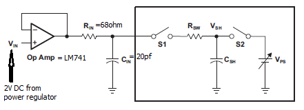
This is not working. ADC result register is producing random value (means capacitor Csh is not charging).
I'm including some steps of my code, is't right or want to change something.
Step1: (Buffer circuit)
I'm using Op-amp=LM741, Rin=68ohm, Csh=20pf, Vin=2V DC from power regulator,
Step2: (Clock setting of all)
SYSCLKOUT = 100MHz,
HSPCLK = 50MHz,
ADCCLK = 12.5MHz, (i.e ADCCLKPS=2, CPS=0,)
ACQ_PS=1,
S/H = 160ns, (i.e S/H=(1+ACQ_PS)*time of ADCCLK,)
Steps3: (ePWM_SOC setting)
TBPRD = 10000, (i.e PWM frequency=5000KHz)
CMP = 6000, (i.e 60% duty cycle)
ETSEL.SOCAEN = EPWMA1SOCA_ENABLE,
ETSEL.SOCASEL = PERIOD_EVENT_SELECT,
ETPS.SOCAPRD = GENERATE_1st_EVENT,
Devin,
Presently i saw one thing in silicon_errata.pdf that,
The marker line defined, the B revision device (like TMS320F2808) has been fixed. It means the [ACQ_PS] register bit fixed inside ADC module H/W,
not require to change the bit value in S/W. (ACQ_PS = defult setting for TMS320F2808 board)
## Output of op-amp circuit working well and not oscillating.