This thread has been locked.

If you have a related question, please click the "Ask a related question" button in the top right corner. The newly created question will be automatically linked to this question.

ADCOFFTRIM and Device_Cal TMS320F28034

Other Parts Discussed in Thread: CONTROLSUITE

When we don't call Device_Cal and use EALLOW to read the ADCOFFTRIM register the value is 0.  The A/D gives accurate results (at room temperature).  However, if we invoke the Device_Cal and read the ADCOFFTRIM register we get a non zero value (x).

Now all the A/D readings (digital) are offset by x.  For example, if the non Devcie_Cal A/D reading was 100, the invoked reading yields an ADCOFFTRIM of 14, then the A/D reading is now 114. 

Are we suppose to subtract the ADCOFFTRIM from our readings or is this inherently done within the A/D?

  • Hi Elliott,

    This is the intended operation of the offset trim register...it globally adds or subtracts an offset to all ADC conversions. This is to compensate for offset error in the ADC and board.

    However, we don't actually recommend that you use the offset provided in the device calibration function. Instead, you need to either do a one-time or periodic offset self-calibration for each device. How to do this is documented in the ADC user guide, spruge5f, in section 1.8.2 "ADC Zero Offset Calibration". You can also look at some provided example code in ControlSUITE: void AdcOffsetSelfCal() in .\controlSUITE\device_support\f2803x\v130\DSP2803x_common\source\DSP2803x_Adc.c. Note that how you integrate the self-calibration into your application code can vary, and changing the ADC setup in one place can have side-effects for the rest of your ADC sampling code, so don't take the provided example as a call-and-forget library, but instead truly use it as an example.

    As far as performance with one-time vs. periodic self-calibration, we specify both in the device datasheet in Table 6-29 "ADC Electrical Characteristics". Note that we don't specify any performance with the default offset trim values.
  • Thank you for your info. We are doing what you suggested. My question is when you run Device_Cal on startup, we get an OFFTRIM value of say 10, when we read our A/D readings they are all off by 10, if we don't run Device_Cal and the OFFTRIM is 0, the readings are correct. So the question was are we suppose to subtract this offset or I assume it is done automatically in the A/D core? If so, then what is the explanation for this?

    Regards,
    Scott Elliott
  • Hi Scott,

    The OFFTRIM value from device_cal will get completely overwritten by whatever you come up with when doing self calibration. No need to factor it in in any way.
  • Thanks for you input, I do understand when we run Device_Cal the register will be overwritten. That's not the issue, the issue is when we run Device_Cal it uses the factory offset and that offset value is actually causing the A/D readings to be off by that amount. If we don't run the Device_Cal and leave the register (OFFTRIM) zero, the A/D readings are dead on.

    Why is this?

    Regards,
    Scott Elliott
  • Hi Scott, ADC offset is highly dependent on system HW.  The factory trim used in Device_Cal is based on the HW in the manufacturing environment which may or may not correlate to a customer board.  This is why self-cal is required and results using Device_Cal should be ignored.  For this particular device in this particular system, it appears the needed trim is ~0 but when that device was tested in the manufacturing environment, a different value was required to cancel the offset error which is needed for proper gain error trim and testing. 

    Regards,

    Joe

  • Joe,

    I guess I'm not making myself very clear. It's doesn't matter which method we use (1) Device_Cal then (2) Auto_Cal, if the offsettrim is non-zero it is added to the A/D readings which results in wrong values. For example:

    1. Don't use Device_Cal or AutoCal so OFFTRIM = 0, all our A/D readings are valid and within spec.
    2. Use Device_Cal and get an offset of 19, now all our A/D readings have 19 added, which results in not in spec.
    3. Use Device_Cal and then AutoCal and get a OFFTRIM = 5, A/D readings have 5 added, which results in out of spec compared to test case 1 above.

    We do a offset test where we introduce a 30 mv into the A/D and as long we have OFFTRIM = 0 the A/D readings are dead on. If we use test case 2 or 3 above the A/D readings are 30 mv plus the OFFTRIM.

    I hope this is now clear and you can provide more info on what's going on.

    Regards,
    Scott Elliott

    Use Device_Cal get a offset of 19
  • OK sorry we seem to keep talking past each other. Can you specify what conversion results you are getting when they are "dead on"? I am just trying to clarify whether you are using the results of (1) or actual expected conversion results based on the input voltage as "golden".
    It might also help us to know the following:
    * what you are using to force the voltage on the input?
    * are you measuring the voltage at the pin or trusting the source output reading?
    * is it buffered?
    * what ACQPS and ADCCLK settings are you using?
    * are you taking multiple samples and averaging or single conversions?
    Joe
  • Joe,
    We run what are in the TI libraries.
    Scott
    //###########################################################################
    //
    // FILE: DSP2803x_Adc.c
    //
    // TITLE: DSP2803x ADC Initialization & Support Functions.
    //
    //###########################################################################
    // $TI Release: F2803x C/C++ Header Files and Peripheral Examples V126 $
    // $Release Date: November 30, 2011 $
    //###########################################################################
    // Modifications, derivations, and improvements are Copyright © 2016 By LORD Corporation
    // Baseline code developed by: Codeskin
    // Updates:
    // 08/2016: Added ADC periodic calibration.
    //###########################################################################
    #include "includes.h"
    #include "DSP2803x_Device.h" // DSP2803x Headerfile Include File
    #include "DSP2803x_usDelay.h"
    #include "sci.h"

    /**
    * @brief Pointer to a function to calibrates the ADC and internal oscillators.
    *
    * Parenthesis intentionally left open for the user to complete.
    */
    #define Device_cal (void (*)(void))0x3D7C80


    #define ADC_usDELAY 1000L

    //---------------------------------------------------------------------------
    // InitAdc:
    //---------------------------------------------------------------------------
    // This function initializes ADC to a known state.
    //
    // NOTE: ADC INIT IS DIFFERENT ON 2803x DEVICES COMPARED TO OTHER 28X DEVICES
    //
    // *IMPORTANT*
    // IF RUNNING FROM FLASH, PLEASE COPY OVER THE SECTION "ramfuncs" FROM FLASH
    // TO RAM PRIOR TO CALLING InitSysCtrl(). THIS PREVENTS THE MCU FROM THROWING
    // AN EXCEPTION WHEN A CALL TO DELAY_US() IS MADE.
    //
    void InitAdc(void)
    {
    // *IMPORTANT*
    // The Device_cal function, which copies the ADC calibration values from TI reserved
    // OTP into the ADCREFSEL and ADCOFFTRIM registers, occurs automatically in the
    // Boot ROM. If the boot ROM code is bypassed during the debug process, the
    // following function MUST be called for the ADC to function according
    // to specification. The clocks to the ADC MUST be enabled before calling this
    // function.
    // See the device data manual and/or the ADC Reference
    // Manual for more information.

    EALLOW;
    SysCtrlRegs.PCLKCR0.bit.ADCENCLK = 1;
    (*Device_cal)();
    EDIS;

    // To powerup the ADC the ADCENCLK bit should be set first to enable
    // clocks, followed by powering up the bandgap, reference circuitry, and ADC core.
    // Before the first conversion is performed a 5ms delay must be observed
    // after power up to give all analog circuits time to power up and settle
    EALLOW;
    AdcRegs.ADCCTL1.bit.ADCBGPWD = 1; // Power ADC BG
    AdcRegs.ADCCTL1.bit.ADCREFPWD = 1; // Power reference
    AdcRegs.ADCCTL1.bit.ADCPWDN = 1; // Power ADC
    AdcRegs.ADCCTL1.bit.ADCENABLE = 1; // Enable ADC
    AdcRegs.ADCCTL1.bit.ADCREFSEL = 0; // Select interal BG
    EDIS;

    DELAY_US(ADC_usDELAY); // Delay before converting ADC channels
    }

    void InitAdcAio()
    {

    EALLOW;

    /* Configure ADC pins using AIO regs*/
    // This specifies which of the possible AIO pins will be Analog input pins.
    // NOTE: AIO1,3,5,7-9,11,13,15 are analog inputs in all AIOMUX1 configurations.
    // Comment out other unwanted lines.

    GpioCtrlRegs.AIOMUX1.bit.AIO2 = 2; // Configure AIO2 for A2 (analog input) operation
    GpioCtrlRegs.AIOMUX1.bit.AIO4 = 2; // Configure AIO4 for A4 (analog input) operation
    GpioCtrlRegs.AIOMUX1.bit.AIO6 = 2; // Configure AIO6 for A6 (analog input) operation
    GpioCtrlRegs.AIOMUX1.bit.AIO10 = 2; // Configure AIO10 for B2 (analog input) operation
    GpioCtrlRegs.AIOMUX1.bit.AIO12 = 2; // Configure AIO12 for B4 (analog input) operation
    GpioCtrlRegs.AIOMUX1.bit.AIO14 = 2; // Configure AIO14 for B6 (analog input) operation

    EDIS;
    }


    /* AdcChanSelect-
    This function selects the ADC channel to convert by setting all SOC channel selects to a single channel.

    * IMPORTANT * This function will overwrite previous SOC channel select settings. Recommend saving
    the previous settings.
    */
    void AdcChanSelect(Uint16 ch_no)
    {
    AdcRegs.ADCSOC0CTL.bit.CHSEL= ch_no;
    AdcRegs.ADCSOC1CTL.bit.CHSEL= ch_no;
    AdcRegs.ADCSOC2CTL.bit.CHSEL= ch_no;
    AdcRegs.ADCSOC3CTL.bit.CHSEL= ch_no;
    AdcRegs.ADCSOC4CTL.bit.CHSEL= ch_no;
    AdcRegs.ADCSOC5CTL.bit.CHSEL= ch_no;
    AdcRegs.ADCSOC6CTL.bit.CHSEL= ch_no;
    AdcRegs.ADCSOC7CTL.bit.CHSEL= ch_no;
    AdcRegs.ADCSOC8CTL.bit.CHSEL= ch_no;
    AdcRegs.ADCSOC9CTL.bit.CHSEL= ch_no;
    AdcRegs.ADCSOC10CTL.bit.CHSEL= ch_no;
    AdcRegs.ADCSOC11CTL.bit.CHSEL= ch_no;
    AdcRegs.ADCSOC12CTL.bit.CHSEL= ch_no;
    AdcRegs.ADCSOC13CTL.bit.CHSEL= ch_no;
    AdcRegs.ADCSOC14CTL.bit.CHSEL= ch_no;
    AdcRegs.ADCSOC15CTL.bit.CHSEL= ch_no;
    } //end AdcChanSelect*/

    /* AdcConversion -
    This function initiates several ADC conversions and returns the average. It uses ADCINT1 and ADCINT2
    to "ping-pong" between SOC0-7 and SOC8-15 and is referred to as "ping-pong" sampling.

    * IMPORTANT * This function will overwrite previous ADC settings. Recommend saving previous settings.
    */
    Uint16 AdcConversion(void)
    {
    Uint16 index, SampleSize, Mean, ACQPS_Value;
    Uint32 Sum;

    index = 0; //initialize index to 0
    SampleSize = 256; //set sample size to 256 (**NOTE: Sample size must be multiples of 2^x where is an integer >= 4)
    Sum = 0; //set sum to 0
    Mean = 999; //initialize mean to known value

    //Set the ADC sample window to the desired value (Sample window = ACQPS + 1)
    ACQPS_Value = 6;
    AdcRegs.ADCSOC0CTL.bit.ACQPS = ACQPS_Value;
    AdcRegs.ADCSOC1CTL.bit.ACQPS = ACQPS_Value;
    AdcRegs.ADCSOC2CTL.bit.ACQPS = ACQPS_Value;
    AdcRegs.ADCSOC3CTL.bit.ACQPS = ACQPS_Value;
    AdcRegs.ADCSOC4CTL.bit.ACQPS = ACQPS_Value;
    AdcRegs.ADCSOC5CTL.bit.ACQPS = ACQPS_Value;
    AdcRegs.ADCSOC6CTL.bit.ACQPS = ACQPS_Value;
    AdcRegs.ADCSOC7CTL.bit.ACQPS = ACQPS_Value;
    AdcRegs.ADCSOC8CTL.bit.ACQPS = ACQPS_Value;
    AdcRegs.ADCSOC9CTL.bit.ACQPS = ACQPS_Value;
    AdcRegs.ADCSOC10CTL.bit.ACQPS = ACQPS_Value;
    AdcRegs.ADCSOC11CTL.bit.ACQPS = ACQPS_Value;
    AdcRegs.ADCSOC12CTL.bit.ACQPS = ACQPS_Value;
    AdcRegs.ADCSOC13CTL.bit.ACQPS = ACQPS_Value;
    AdcRegs.ADCSOC14CTL.bit.ACQPS = ACQPS_Value;
    AdcRegs.ADCSOC15CTL.bit.ACQPS = ACQPS_Value;


    //Enable ping-pong sampling

    // Enabled ADCINT1 and ADCINT2
    AdcRegs.INTSEL1N2.bit.INT1E = 1;
    AdcRegs.INTSEL1N2.bit.INT2E = 1;

    // Disable continuous sampling for ADCINT1 and ADCINT2
    AdcRegs.INTSEL1N2.bit.INT1CONT = 0;
    AdcRegs.INTSEL1N2.bit.INT2CONT = 0;

    AdcRegs.ADCCTL1.bit.INTPULSEPOS = 1; //ADCINTs trigger at end of conversion

    // Setup ADCINT1 and ADCINT2 trigger source
    AdcRegs.INTSEL1N2.bit.INT1SEL = 6; //EOC6 triggers ADCINT1
    AdcRegs.INTSEL1N2.bit.INT2SEL = 14; //EOC14 triggers ADCINT2

    // Setup each SOC's ADCINT trigger source
    AdcRegs.ADCINTSOCSEL1.bit.SOC0 = 2; //ADCINT2 starts SOC0-7
    AdcRegs.ADCINTSOCSEL1.bit.SOC1 = 2;
    AdcRegs.ADCINTSOCSEL1.bit.SOC2 = 2;
    AdcRegs.ADCINTSOCSEL1.bit.SOC3 = 2;
    AdcRegs.ADCINTSOCSEL1.bit.SOC4 = 2;
    AdcRegs.ADCINTSOCSEL1.bit.SOC5 = 2;
    AdcRegs.ADCINTSOCSEL1.bit.SOC6 = 2;
    AdcRegs.ADCINTSOCSEL1.bit.SOC7 = 2;
    AdcRegs.ADCINTSOCSEL2.bit.SOC8 = 1; //ADCINT1 starts SOC8-15
    AdcRegs.ADCINTSOCSEL2.bit.SOC9 = 1;
    AdcRegs.ADCINTSOCSEL2.bit.SOC10 = 1;
    AdcRegs.ADCINTSOCSEL2.bit.SOC11 = 1;
    AdcRegs.ADCINTSOCSEL2.bit.SOC12 = 1;
    AdcRegs.ADCINTSOCSEL2.bit.SOC13 = 1;
    AdcRegs.ADCINTSOCSEL2.bit.SOC14 = 1;
    AdcRegs.ADCINTSOCSEL2.bit.SOC15 = 1;

    DELAY_US(ADC_usDELAY); // Delay before converting ADC channels

    //ADC Conversion

    AdcRegs.ADCSOCFRC1.all = 0x00FF; // Force Start SOC0-7 to begin ping-pong sampling

    while( index < SampleSize ){

    //Wait for ADCINT1 to trigger, then add ADCRESULT0-7 registers to sum
    while (AdcRegs.ADCINTFLG.bit.ADCINT1 == 0){}
    AdcRegs.ADCINTFLGCLR.bit.ADCINT1 = 1; //Must clear ADCINT1 flag since INT1CONT = 0
    Sum += AdcResult.ADCRESULT0;
    Sum += AdcResult.ADCRESULT1;
    Sum += AdcResult.ADCRESULT2;
    Sum += AdcResult.ADCRESULT3;
    Sum += AdcResult.ADCRESULT4;
    Sum += AdcResult.ADCRESULT5;
    Sum += AdcResult.ADCRESULT6;
    Sum += AdcResult.ADCRESULT7;

    //Wait for ADCINT2 to trigger, then add ADCRESULT8-15 registers to sum
    while (AdcRegs.ADCINTFLG.bit.ADCINT2 == 0){}
    AdcRegs.ADCINTFLGCLR.bit.ADCINT2 = 1; //Must clear ADCINT2 flag since INT2CONT = 0
    Sum += AdcResult.ADCRESULT8;
    Sum += AdcResult.ADCRESULT9;
    Sum += AdcResult.ADCRESULT10;
    Sum += AdcResult.ADCRESULT11;
    Sum += AdcResult.ADCRESULT12;
    Sum += AdcResult.ADCRESULT13;
    Sum += AdcResult.ADCRESULT14;
    Sum += AdcResult.ADCRESULT15;

    index+=16;

    } // end data collection

    //Disable ADCINT1 and ADCINT2 to STOP the ping-pong sampling
    AdcRegs.INTSEL1N2.bit.INT1E = 0;
    AdcRegs.INTSEL1N2.bit.INT2E = 0;

    Mean = Sum / SampleSize; //Calculate average ADC sample value

    return Mean; //return the average

    }//end AdcConversion

    /**
    * ADC Offset Self Calibration.
    *
    * This function re-calibrates the ADC zero offset error by converting the VREFLO reference with
    * the ADC and modifying the ADCOFFTRIM register. VREFLO is sampled by the ADC using an internal
    * MUX select which connects VREFLO to A5 without sacrificing an external ADC pin.
    */
    void AdcOffsetSelfCal(void)
    {
    Uint16 AdcConvMean;
    const Uint16 ch_no = 13U; // Select channel B5 for all SOC.
    const Uint16 artificial_offset = 80U; // Offset to account for a negative offset that may reside in the ADC core.

    EALLOW;
    AdcRegs.ADCCTL1.bit.ADCREFSEL = 0; // Select internal reference mode.
    AdcRegs.ADCCTL1.bit.VREFLOCONV = 1; // Select VREFLO internal connection on B5.

    AdcChanSelect(ch_no);

    AdcRegs.ADCSOC0CTL.bit.CHSEL= ch_no;
    AdcRegs.ADCSOC1CTL.bit.CHSEL= ch_no;
    AdcRegs.ADCSOC2CTL.bit.CHSEL= ch_no;
    AdcRegs.ADCSOC3CTL.bit.CHSEL= ch_no;
    AdcRegs.ADCSOC4CTL.bit.CHSEL= ch_no;
    AdcRegs.ADCSOC5CTL.bit.CHSEL= ch_no;
    AdcRegs.ADCSOC6CTL.bit.CHSEL= ch_no;
    AdcRegs.ADCSOC7CTL.bit.CHSEL= ch_no;
    AdcRegs.ADCSOC8CTL.bit.CHSEL= ch_no;
    AdcRegs.ADCSOC9CTL.bit.CHSEL= ch_no;
    AdcRegs.ADCSOC10CTL.bit.CHSEL= ch_no;
    AdcRegs.ADCSOC11CTL.bit.CHSEL= ch_no;
    AdcRegs.ADCSOC12CTL.bit.CHSEL= ch_no;
    AdcRegs.ADCSOC13CTL.bit.CHSEL= ch_no;
    AdcRegs.ADCSOC14CTL.bit.CHSEL= ch_no;
    AdcRegs.ADCSOC15CTL.bit.CHSEL= ch_no;

    AdcRegs.ADCOFFTRIM.bit.OFFTRIM = artificial_offset; //Apply artificial offset.

    AdcConvMean = AdcConversion(); //Capture ADC conversion on VREFLO
    /*
    * Set offtrim register with new value (i.e remove artical offset and create a two's compliment of the offset error)
    */
    AdcRegs.ADCOFFTRIM.bit.OFFTRIM = artificial_offset - AdcConvMean;
    AdcRegs.ADCCTL1.bit.VREFLOCONV = 0; //Select external ADCIN5 input pin on B5.

    EDIS;
    }

    //===========================================================================
    // End of file.
    //===========================================================================
  • Also, if we just run the device cal and check the register of the OFFTRIM and it is 35 or 37 doesn't this imply the chip is out of spec?

    We have two units that w/o auto self cal, the Devcie_Cal returns a 35 and 37, isn't 20 the upper limit?
    EALLOW;
    SysCtrlRegs.PCLKCR0.bit.ADCENCLK = 1;
    (*Device_cal)();
    EDIS;
  • Hi Elliott,

    (a quick response to your most recent post)

    To be very clear: the trim populated by Device_cal is garbage, just ignore it. This is why we require self-calibration.

    The DS spec' is for the offset error, not the value of the offset trim. With one-time trim, you should see offset error of no more than +/-20 LSBs over operating conditions. With periodic trim, you should see +/- 4 LSBs of offset error over operating conditions. There is no specification for performance without self-trim; this includes when using the factory trim in the Device_cal function.

    The range of the offset trim I believe is +63/-64, so you should only be concerned if your self-trim is producing values near these extremes. This would indicate that the natural device offset + board parasitic offset is too large to calibrate out.
  • Hi Elliot,


    One more thing to check is if you have set the ADC clock divider to /2 and if you have enabled non-overlap mode?  There are some ADC errata that may be relevant when running in other modes, so you may want to try adding these configurations somewhere in your initializations before you do offset self-calibration. 

  • Hi Joe:
    could u pls. further explain what writing to the OFFTRIM register does to all ADC lines? I performed the following:
    - Performed our own startup ADC calibration by setting the OFFTRIM register value to 80 (per TI's suggestion).
    - Then we read off two ADC lines that are connected to ground 10 times and take the average.
    - We subtract this average from 80 to determine what the ADC correction factor is (if correction factor is negative, we write the abs value to the OFFTRIM register, and if positive, we write the twos complement of the negative correction factor to the OFFTRIM register).
    - I proceeded to verify this by inducing a smaller offset (+30) to the OFFTRIM register then reading back what the ground ADC lines were and they are both reading different values.

    So, questions are the following:
    - if two lines are connected to ground, i expected both to show same numbers at the end when i induced a +30 offset.
    - is my procedure for our calibration right?

    Thanks for the help,
    Abe
  • Hi Abe,

    If the artificial offset error is +80, and your average reading is 90, then you want to load -10 into the OFFTRIM register. Doing 80-avg gives you the correct result; no need to take abs or invert further.

    If the calculated offset was greater than -30, then if you load +30 into the offset trim register and repeat the averaging process 30 - avg2 should be pretty close to what you got the first time using 80 - avg1. Note that we specify a channel-to-channel offset variation of +/-4 LSBs, so you may not see the exact same result on 2 different channels. Noise could also contribute to run-to-run variation (you may want to do a larger average, say 256 samples).

    Whatever final procedure you use should keep the calculated offset trim in the OFFTRIM register (and not overwrite it with an artificial offset trim like +30)
  • Just want to confirm that when u load -10 into the OFFTRIM Register, i would have to put it into 2's complement correct?

    Thanks for the help.
  • Hi Abe,

    Yes, the -10 would be in 2's compliment format.

    You wouldn't want to take the 2's compliment of -10 though, because that would give you +10. 2's compliment is the format naturally used by signed data types in CCS like int16 or int32, so you don't really have to do anything other than load -10 into the OFFTRIM register.
  • We are getting close to concluding this exercise.

    While investigating this, we discovererd that one of the principal causes of noise in our system was the configuration parameter ADCNONOVERLAP.

    This parameter allows some (as far as I can tell, unspecified) overlap between the end of the sampling period and the start of the ADC conversion period.

    In the presence of a noisy signal, I can see that starting a pipelined ADC conversion while the input signal is changing could introduce additional errors into the ADC process.   I'm having difficulty understanding why you would ever want to have overlap between sampling and conversion.   Please can you answer the following questions:

    (1) Am I correctly understanding what the ADCNONOVERLAP register causes during the ADC cycle?

    (2) How much overlap between sample and conversion does clearing ADCNONOVERLAP to 0 cause?

    (3) Why would anyone want to have overlap between the sample and the convert cycles of a high speed ADC?

    Thanks

    Jeff

  • Hi Jeff,

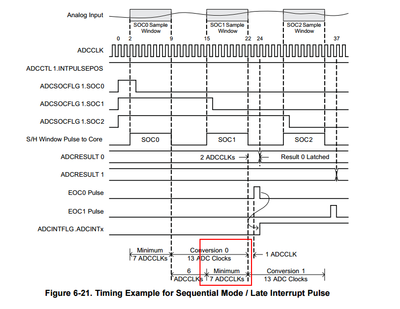
    The architecture of the ADC for this device is "Hybrid pipeline / SAR".  The original design allowed some level of pipelining between the conversion phase of one conversion, and the S+H phase of the next conversion.  This is up to 7 ADCCLK cycles, and can be seen in the following timing diagrams:

    This architecture is theoretically fine; many high speed ADCs use a pipelined architecture (and almost all really high speed ADCs).  However, we have an errata for this device (first sample issue) which was solved by adding the functionality to allow the user to disable conversion pipelining (writing 1 to the ADCNONOVERLAP bit) and by setting the ADC clock speed to 30MHz.

    It is recommended to do your offset self-calibration with identical settings to whatever your application is going to use (so if you intend to enable the NONOVERLAP bit and run at 30MHz to avoid the 1st sample issue, these settings would be the best choices for also doing self-calibration).