This thread has been locked.

If you have a related question, please click the "Ask a related question" button in the top right corner. The newly created question will be automatically linked to this question.

AMC1304M25 Delta Sigma Modulator Interface with SDFM (TMS320F28377S)

Other Parts Discussed in Thread: AMC1304M25, CONTROLSUITE, TMS320F28377S, TCAN337


Hi,

I am using AMC1304M25 Delta Sigma Modulator to implement shunt current measurements. The filter module is used from on chip SDFM peripheral from TMS320F28377S Launchpad. For this, I edited an example already available in ControlSuite for interrupt based SDFM: sdfm_filters_sync_cpu.

I want to use only one channel of SDFM1 at the moment where the signal acquisition source is function generator.

The edited code is given below:

//###########################################################################
// FILE:   sdfm_pwm_sync_cpu_cpu01.c
// TITLE:  SDFM PWM sync Example for F2837xS.
//
//! \addtogroup cpu01_example_list
//! <h1> SDFM PWM Sync </h1>
//!
//###########################################################################
#include "F28x_Project.h"
#include "F2837xS_struct.h"
#include "F2837xS_sdfm_drivers.h"
//*****************************************************************************
// Macro definitions
//*****************************************************************************
#define MAX_SAMPLES  1024
#define SDFM_PIN_MUX_OPTION1        1    // only GPIO 16 and GPIO 17 are configured
#define SDFM_PIN_MUX_OPTION2        2
//*****************************************************************************
// Global variables
//*****************************************************************************
uint16_t gPeripheralNumber;       // SDFM1
// Configure the period for each timer
#define EPWM11_TIMER_TBPRD  9  // Period register
#define EPWM11_CMPA     4
#define EPWM11_CMPB     4
#define latency 77
uint16_t  Filter1_Result[MAX_SAMPLES];
//*****************************************************************************
#pragma DATA_SECTION(Filter1_Result,"Filter1_RegsFile");
void Sdfm_configurePins(uint16_t);
void InitEPwm11Example(void);     // ePWM 11 Clock signal and filter sync
void done(void);
__interrupt void Sdfm1_ISR(void);
 
void main(void)
{
       // initialize filter with value 1
       unsigned int i=0;
       for (i = 0; i < MAX_SAMPLES; i++)
       {
             Filter1_Result[i]=1;
       }
 
   uint16_t   pinMuxoption;
   uint16_t  HLT, LLT;     // to store threshold values
 
   InitSysCtrl();
 
   // for ePWM module
   EALLOW;
   ClkCfgRegs.PERCLKDIVSEL.bit.EPWMCLKDIV = 0x0;      // set ePWM divider to /1
   EDIS;
   //
   CpuSysRegs.PCLKCR2.bit.EPWM11 = 1;
   //
   InitGpio();
   //************************Initialize PWM 11A/B GPIO************
   GPIO_SetupPinMux(20, GPIO_MUX_CPU1, 5);
   GPIO_SetupPinOptions(20, GPIO_OUTPUT, GPIO_PUSHPULL);
   GPIO_SetupPinMux(21, GPIO_MUX_CPU1, 5);
   GPIO_SetupPinOptions(21, GPIO_OUTPUT, GPIO_PUSHPULL);
   //**************************************************************
// Disable CPU __interrupts
   DINT;
 
// Initialize PIE control registers to their default state.
   InitPieCtrl();
 
// Disable CPU __interrupts and clear all CPU __interrupt flags:
   IER = 0x0000;
   IFR = 0x0000;
 
// Initialize the PIE vector table with pointers to the shell Interrupt
// Service Routines (ISR).
   InitPieVectTable();
 
// Interrupts that are used in this example are re-mapped to
// ISR functions found within this file.
       EALLOW;
       PieVectTable.SD1_INT = &Sdfm1_ISR;
       // Enable CPU INT5 which is connected to SDFM INT
       IER |= M_INT5;
       EDIS;
 
       // Enable SDFM INTn in the PIE: Group 5 __interrupt 9-10
       PieCtrlRegs.PIEIER5.bit.INTx9 = 1;      // SDFM1 interrupt enabled
       //
       // initialize ePWM11
       EALLOW;
       CpuSysRegs.PCLKCR0.bit.TBCLKSYNC =0;
       EDIS;
 
       InitEPwm11Example();
 
       EALLOW;
       CpuSysRegs.PCLKCR0.bit.TBCLKSYNC =1;
       EDIS;
       //
       EINT;
       //
       pinMuxoption = SDFM_PIN_MUX_OPTION1;
       // Configure GPIO pins as SDFM pins
       Sdfm_configurePins(pinMuxoption);
       //Select SDFM1
       gPeripheralNumber = SDFM1;
       /*******************************************************/
       /* Input Control Module */
       /*******************************************************/
       //Configure Input Control Mode: Modulator Clock rate = Modulator data rate
       Sdfm_configureInputCtrl(gPeripheralNumber, FILTER1, MODE_0);
       /*******************************************************/
       /* Comparator Module */
       /*******************************************************/
       HLT = 0x7FFF;    //Over value threshold settings
    LLT = 0x0000;    //Under value threshold settings
 
       //Configure Comparator module's comparator filter type and comparator's OSR value, higher threshold, lower threshold
       Sdfm_configureComparator(gPeripheralNumber, FILTER1, SINC3, OSR_32, HLT, LLT);
 
       /*******************************************************/
       /* Data filter Module */
       /*******************************************************/
       //Configure Data filter modules filter type, OSR value and enable / disable data filter
       Sdfm_configureData_filter(gPeripheralNumber, FILTER1, FILTER_ENABLE, SINC3, OSR_256, DATA_16_BIT, SHIFT_9_BITS);
 
       // External reset are disabled
    Sdfm_configureExternalreset(gPeripheralNumber,FILTER_1_EXT_RESET_DISABLE, FILTER_2_EXT_RESET_DISABLE, FILTER_3_EXT_RESET_DISABLE, FILTER_4_EXT_RESET_DISABLE);
 
       /*******************************************************/
       /* Enable interrupts */
       /*******************************************************/
       Sdfm_configureInterrupt(gPeripheralNumber, FILTER1, IEH_ENABLE, IEL_ENABLE, MFIE_ENABLE, AE_ENABLE);
 
       Sdfm_enableMFE(gPeripheralNumber);      // enable Module filters
       DELAY_US(latency);                             // to avoid spurious interrupts
       Sdfm_enableMIE(gPeripheralNumber);
 
       while(1);
}
 
__interrupt void Sdfm1_ISR(void)
{
       uint32_t sdfmReadFlagRegister =0;
       static uint16_t loopCounter1 = 0;
 
       // Read SDFM flag register (SDIFLG)
       sdfmReadFlagRegister = Sdfm_readFlagRegister(gPeripheralNumber);
 
       if(loopCounter1 <= MAX_SAMPLES)
       {
             // Read each SDFM filter output and store it in respective filter result array
             Filter1_Result[loopCounter1++] = SDFM1_READ_FILTER1_DATA_16BIT;
 
             // Clear SDFM flag register
             Sdfm_clearFlagRegister(gPeripheralNumber,sdfmReadFlagRegister);    // setting clrflag register to zero !
             sdfmReadFlagRegister = Sdfm_readFlagRegister(gPeripheralNumber);   // reading flag register to see if INT is cleared
             if(sdfmReadFlagRegister != 0x0)   // if INT is still active
             {
                    ESTOP0;
             }
       }
       else
       {
             ESTOP0;
             done();
       }
       // Acknowledge this __interrupt to receive more __interrupts from group 5
       PieCtrlRegs.PIEACK.all = PIEACK_GROUP5;
}
 
void Sdfm_configurePins(uint16_t sdfmPinOption)
{
       uint16_t pin;
       switch (sdfmPinOption)
       {
             case SDFM_PIN_MUX_OPTION1:
                    for(pin=16;pin<=17;pin++)
                    {
                           GPIO_SetupPinOptions(pin, GPIO_INPUT, GPIO_ASYNC);    // Configure GPIOs as asynchronous input
                           GPIO_SetupPinMux(pin,GPIO_MUX_CPU1,7);                       // Configure this pin to be owned by CPU1 and configure this pin as SDFM pin
                    }
                    break;
 
             case SDFM_PIN_MUX_OPTION2:
                    for(pin=18;pin<=19;pin++)
                    {
                           GPIO_SetupPinOptions(pin, GPIO_INPUT, GPIO_ASYNC);
                           GPIO_SetupPinMux(pin,GPIO_MUX_CPU1,7);
                    }
                    break;
       }
 
}
 
void InitEPwm11Example(void)
{
   // Setup TBCLK
   EPwm11Regs.TBCTL.bit.CTRMODE = TB_COUNT_UP; // Count up
   EPwm11Regs.TBPRD = EPWM11_TIMER_TBPRD;       // Set timer period
   EPwm11Regs.TBCTL.bit.PHSEN = TB_DISABLE;    // Disable phase loading
   EPwm11Regs.TBPHS.bit.TBPHS = 0x0000;       // Phase is 0
   EPwm11Regs.TBCTR = 0x0000;                  // Clear counter
   EPwm11Regs.TBCTL.bit.HSPCLKDIV = TB_DIV1;   // Clock ratio to SYSCLKOUT
   EPwm11Regs.TBCTL.bit.CLKDIV = TB_DIV2;
 
   // Setup shadow register load on ZERO
   EPwm11Regs.CMPCTL.bit.SHDWAMODE = CC_SHADOW;
   EPwm11Regs.CMPCTL.bit.SHDWBMODE = CC_SHADOW;
//   EPwm11Regs.CMPCTL2.bit.SHDWCMODE = CC_SHADOW;
   EPwm11Regs.CMPCTL.bit.LOADAMODE = CC_CTR_ZERO;
   EPwm11Regs.CMPCTL.bit.LOADBMODE = CC_CTR_ZERO;
//   EPwm11Regs.CMPCTL2.bit.LOADCMODE = CC_CTR_ZERO;
 
   // Set Compare values
   EPwm11Regs.CMPA.bit.CMPA = EPWM11_CMPA;    // Set compare A value
   EPwm11Regs.CMPB.bit.CMPB = EPWM11_CMPB;              // Set Compare B value
 
   // Set actions
//   EPwm1Regs.AQCTLA.bit.ZRO = AQ_SET;            // Set PWM1A on Zero
//   EPwm1Regs.AQCTLA.bit.CAU = AQ_CLEAR;          // Clear PWM1A on event A, up count
   EPwm11Regs.AQCTLA.bit.PRD = AQ_CLEAR;
   EPwm11Regs.AQCTLA.bit.CAU = AQ_SET;
 
//   EPwm1Regs.AQCTLB.bit.ZRO = AQ_SET;            // Set PWM1B on Zero
//   EPwm1Regs.AQCTLB.bit.CBU = AQ_CLEAR;          // Clear PWM1B on event B, up count
   EPwm11Regs.AQCTLB.bit.PRD = AQ_CLEAR;
   EPwm11Regs.AQCTLB.bit.CAU = AQ_SET;
 
   //Setting CMPC sync settings
//   EPwm11Regs.CMPC = EPWM11_TIMER_TBPRD;
}
 
void done(void)
{
       asm(" ESTOP0");
       for (;;);
}
//

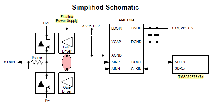
Same clock signals PWM11A and PWM11B (10MHz) are supplied to SD_Cx and AMC1304M25 modulator. Latter is also supplied with 5VDC.
The clock signal and data stream seen at delta sigma modulator pins CLK_IN and DOUT are
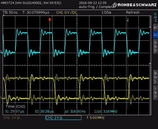
Data stream (yellow) seems to have half frequency to that of clock signal (blue).
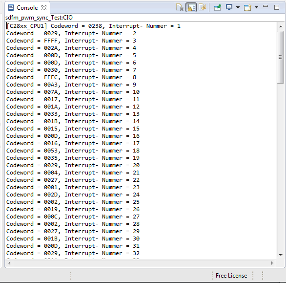
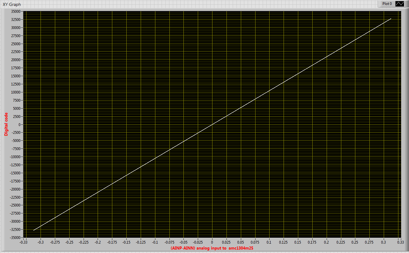
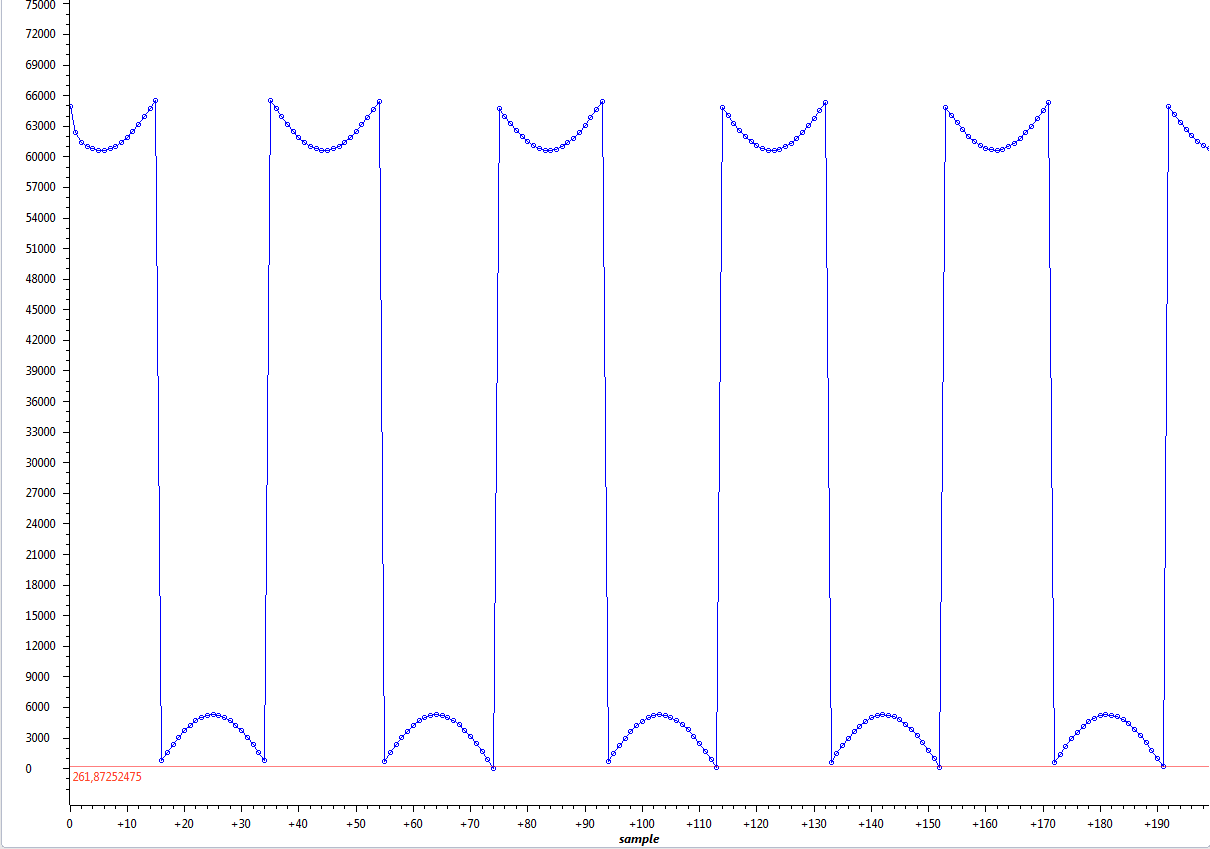
The problem is that when I supply 400mVpeak-peak Signal from function generator centered around zero axis. The values that get stored in Filter Matrix are strange and their two's complement yields strange output voltages.
For example: Function generator Sine wave 400mVpeak-peak, Frequency 1KHz, Sine wave yields following matrix values
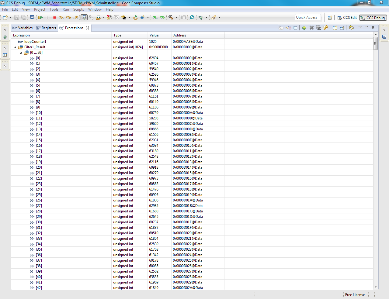
Similarly, Function generator sine wave with 100mVpeak-peak having same frequency doesnt seem considerably different
In addition, for HLT 0x7FFF, higher threshold Interrupt is only triggered when I supply a sine wave of around 1100mVpeak-peak. I am not sure if +250mV and -250mV range of my modulator is RMS or Vpeak-peak value.
I have following queries:
1) How can I evaluate if data being converted is correct; I am taking two's complement of data acquired from filter but that doesn't seem to be correct. I read somehwere in application note that input voltage can be obtained by Vin_calc = (Vclipping)*Codeword / Abs(Codewordpeak), but that doesn't fit either.
2) I have tried using synchronization PWM11.CPMC but in that case my filtter matrix only gets ZEROS and program never comes to halt. Do I need to match AMC1304M25 fall edge and SDFM rise edge processings by using any other PWMx and PWM11.CMPC? As I am using only one channel, do I still need to do synchronization using PWM11.CMPC? I want to use interrupts ISR based accesses of Data Filter reads.
3) Even while using Interrupts ISR, do we need to dealy latency period after Acknowledge Interrupt AEx has occured.
Could you help me please. I will be obliged.
Greetings,
Inam
  • Inam,

    1) To confirm your hardware / code setup is correct, first try providing a DC voltage instead of AC voltage. This should provide consistent digital codes.

    For eg: You can providing a DC (0v), you can expect digital codes around 0x4000 to confirm that your setup is correct.

    2) By using filter synchronization option, you can synchronize filter results with respect to PWM cycle. You can achieve correct filter results even without filter sync option. So, this option is not mandatory.

    3) I believe you are talking about delay function provided before you enable master interrupt enable bit. This is required to make sure you don't receive spurious

    comparator / data filter interrupts. Please check erratum for more details.

    Regards,

    Manoj

     
  • Dear Manhoj,

    Thank you for your response.

    Checking Filter output with constant DC voltage is very helpful.

    I checked the data filter output with several different modulator input voltages. The filter seems doing very well with for example 320mv (0x7FFF) and -320mV (0x8000) where the output word always remains constant, but at other constant voltages including zero DC voltage, the output isn't constant and keeps changing.

    Below a snapshot of output codewords at zero volt modulator DC input.

    To me it seems as if I am reading the filter data output at wrong time but as long as I know, in case of SDFM Interrupts, one doesn't need to wait delay of Latency of Filter after the acknowledge filter Interrupt has occured.

    I am reading filter output as soon as I receive data filter acknowledge interrupt. My code is also not so complex and is taken from example controlsuite/sdfm_sync_cpu_cpu01. I am using only one filter channel without PWM synchronization

    Below you find my SDFM routine:

    One more thing, at DC voltages too like AC input modulator voltages, the modulator output doesn't seem to be constant on oscilloscope either. It seems to be swinging in frequency from 3-5 MHZ ( Clock Frequency 10MHz) which I think should also be constant for a DC voltage, as a bitstream should remain same.

    Can you check my previously attached modulator output bitstream from an AC modulator input voltage. Do you think it is normal ?

    Could you give me some other suggestions with which I could solve my problem. It is playing with my nerves.

    I am grateful for your help.

    Regards,

    Inam

  • Inam,

    Your bit streams looks perfectly normal. Even for a DC voltage, you will not get a DC voltage bitstream.

    If you were expecting a constant digital code for DC voltage it is not going to happen. Did you try plotting your test results?

    Regards,
    Manoj
  • Hi Manhoj,

    If you mean plotting them during a debug session, yes I did but as the same values are plotted which I see on screen, it didn't help.

    I apply a positive voltage and therefore the filter output codes should be in the range 0x0000 - 0x7FFF. If I divide 0x7FFF/312d, I get a span of 105 for each 1mV.

    so for a 100mV input DC, I should expect values around 10500 but my output codes are not consistent and not close to this value. I get codes like 0x00XX, 0xFFXX, 0xDXXX, and so on..

    I do not at least expect a code for a negative value having applied +100mV and values aroubd 10500.

    Thanks & Regards.

    Inam

  • I am also surprised to see that even if data_out from DS-Modulator is not connected to SDFM, the controller takes it as -312,5mV and generates a code 0x8000. Therefore, filter Acknowledge interrupts are triggered even if Data_OUT from modulator is not connected. I hope acknowledge interrupts AEx occur depending on clock. Am I right? if yes, do they occur on each rising edge of CLK signal?

    I doubt I am reading filter output at wrong time. I am expecting that AEx Interrupt occurs when filter output data is ready to read but maybe I am not right. Because if AEx Interrupts are caused at every rising edgeof CLK (10MHz), then my CLK period(0,1uS) is way smaller than latency of data filter i-e 76,8uS.

    Kindly correct me if I am wrong
  • Inam,

    16 bit SDFM data filter output is signed output and can be from 0x8000 (-32768) to 0x7FFF (32767) and not from 0x0 to 0x7FFF.


    For +100mv, you should not be getting negative value. Have you made sure your modulated input signal to SDFM isn't noisy. Have you made sure SDFM mode is configured correctly to match SD-modulator mode?

    Regards,

    Manoj

  • Inam,

    When SD-Cx is provided with no SD-Dx, SDFM will strobe no data as low signal. That is the reason why you get 0x8000. This is expected result.

    Also, AFx interrupt is not generated on every rising edge of SD-Cx. It is generated only when new filter data is available to read. If you read filter data on AFx interrupt then you don't need to worry about reading meta-stable data.

    Are you using SDSYNC (FILRESn) from PWM? Also, have you already tried using 32 bit mode?

    Regards,
    Manoj
  • Dear Manhoj,

    Thank you for clearing my doubt about reading SDFM data on interrupt.

    I am not using SDFM in 32 bit mode rather in 16 bit mode. I have tried using FILRES with PWM11.CMPC where I reset the filter every Latency (76,8uS) + 5-SD-Cx cycles (77,3uS for 10Mhz CLK, mode 0, DOSR 256, Sinc3, Sampling rate 39.1 KSps) but it dint help either.

    For +100mv, you should not be getting negative value. Have you made sure your modulated input signal to SDFM isn't noisy. Have you made sure SDFM mode is configured correctly to match SD-modulator mode?

    I connect AINP and AINN of delta sigma modulator with each other and therefore it sets an input voltage of 0mV, but I wonder my output waveforms on SD Modulator SD-Dx are strange. I expect a pulse train of 50% duty cycle with same freuqency as CLK frequency 10Mhz but I get a strange pulse which isn't stable in frequency either (frequency changes continuously between values 2,5Mhz, 3,33Mhz and 5MHz).

    Do you think this is a problem?

    Snapshots on 0mV. (I also tried connecting both to battery with 0V input)

    Your second question is new to me. How can I make sure if SDFM mode matches SD modulator mode? I am using SDFM in mode 0 while SD modulator is provided with 10MHZ clk signal and 0mV analog input. Same CLK feeds SDFM.

    Thank you again for your help.

    Regards,

    Inam

  • Inam,

    I checked the amc1304m25 datasheet, it looks like data can be strobed on every rising edge. So, you can configure SDFM in mode0.

    SD-Dx you get from SD-modulator is actually sigma-delta modulated bit stream and since you get a data signal on every rising edge it must be half the frequency of SD-Cx. The modulated bit-stream can be jubble of 1s and 0s. So, you will not get a constant frequency when you check in oscilloscope.


    Regards,

    Manoj

  • Dear Manhoj,

    Thank you that your Answer helped me to come to the point that I have no problem with my Hardware (delta-Sigma Modulator, I also verified supply voltages on IC's pins).

    My software settings follow as under:

    SDFM: 1

    Input control Mode: Mode0

    Comparator: COSR_32, Sinc3

    Data Filter channel 1: DOSR_256, Sinc3, Data output 16-Bit, Shift Bits_9

    Interrupts Activated: MFIE (modulator clock Fail), AFx (Filter Acknowledge interrupts)

    External Filter Reset (FILRES): Disabled, Filter data rate = Modulator data rate (10Mhz) / DOSR (256) = 39,1KSPS and Latency = SINC3 / Filter Data Rate = 76,8uS

    Clock Frequency: 10Mhz, Same clock signal feeds SDFM and SD-Modulator

    Example:  ControlSuite\....\sdfm_filters_sync_cpu_cpu01

    Modulator Data update on each CLK falling edge.

    SDFM data strobing at each CLK rising edge.

    SDFM ISR Routine reads data on each Acknowledge Interrupt.

    Code is 100% replica of TI example mentioned with channel 2,3,4 commented, therefore exploiting only channel 1.

    Input Signal : a) 0V, both input pins AINP and AINN connected to each other. Expected Output: around 0x0000 and 0xFFFF.

                             b) 100mV from DC power supply. Expected Output: Consistent Values with no negatives (0xFXXX)


    Expected output codes (Negative values are represented in 2's Complement at Filter Output)

    Do you think my software settings and expected evaluation is correct?

    Thanks alot.

    regards,

    Inam

  • Inam,

    If you provide 0v between AINP / AINN, you can expect digital value around 0x0000s (note: you may see both +ve and -ve value around digital value of 0x0000s)

    If you provide 100mv between AINP / AINN, you can expect digital value around 0x28F6 (note: you shouldn't see any negative value).

    Please see the graph attached below. This is theoretical output

  • Hi Manhoj,

    I found the problem which was actually Sigma Delta modulator. I overlooked the connection between analog ground (AGND) and negative analog input pin (AINN). as shown in figure and that is why delta sigma modulator had high noise on Data Ausgang SD_Dx.


    The codewords that I receive from filter now match perfect to the graph we shared over here. A sample sine wave given below

    I am highly obliged to you for your help meanwhile !

    I am interested to know if I use filter reset, will it be better than not using it ? or in which cases for example filter reset is useful?

    I am using SD modulator as shunt current measurements and the acquired data is supposed to be transfered to PC via CAN peripheral (TMS320F28377S) and Can transciever TI_TCAN337