


Hello,
I am trying to interface the F28069 as a controller for a simulated 2 level inverter.
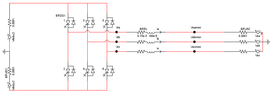
The voltages and currents coming from the simulated two level inverter are per-unitized, offset and scaled to fit within the 0-3.3V input voltage range of the ADC. The F28069 should preform some control algorithm using these voltages and currents and generate the corresponding firing pulses to fire the 6 switches of the bridge using the ePWM modules.
I'm trying to preform a simple open loop test where the controller completely neglects the incoming voltages and currents from the simulation and simply preforms sinusoidal PWM for a fixed modulation index. The value of the modulation index (between 0 and 1) corresponds to the peak value of the sinusoidal modulation waveforms.
I wrote a simple function called Three_Phase_Sinusoid() which generates three phase sinusoids by first generating a peroidic sawtooth waveform from 0 to 2pi, which is then used as the argument to generate a set of three phase sinusoids.
When I run the simulation and the controller, there appears to be low frequency oscillation between the simulation and controller. The simulation outputs new voltages and currents every 100us, and I believe I configured the ADC to trigger every 100us via ePWM7, so I would expect the two to be in synch with eachother.
Here are what the expected waveforms for the voltage and current look like (using a simulated controller),

And here is the low frequency oscillation I observe when the F28069x is acting as the controller,
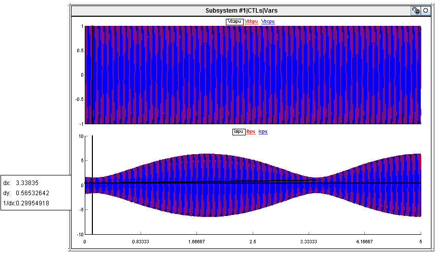
Zoomed in plot of waveforms,

Does anyone have any ideas what the problem could be? My guess was that the execution of the F28069x is not synchronized or executing at a different rate than that of the simulation.
Any ideas?
All of the code for project is shown below.
// Device Headerfile and Examples Include File
#include "DSP28x_Project.h"
#include <math.h>
#include "IQmathLib.h"
#include "ProjDepDef.h" // Device Headerfile and Examples Include File
#include "PeripheralHeaderIncludes.h"
// Prototype statements for functions found within this file.
interrupt void adc_isr(void);
void Three_Phase_Sinusoid(Three_Phase_Sinusoid_Component *this);
// Global variables used in this example:
double dTstep = 0.0001;
FP_VALUE Tstep = 0.0001;
FP_VALUE fADC0 = 0.0;
FP_VALUE fADC1 = 0.0;
FP_VALUE fADC2 = 0.0;
FP_VALUE fADC3 = 0.0;
FP_VALUE fADC4 = 0.0;
FP_VALUE fADC5 = 0.0;
FP_VALUE fPUscale = 0.00024420024;
FP_VALUE freq = 60.0;
FP_VALUE dt = 0.0;
Uint16 dutyA = 0;
Uint16 dutyB = 0;
Uint16 dutyC = 0;
Three_Phase_Sinusoid_Component V;
Uint16 RED_delay=0; // 30=375ns when PLL is set to 0xC (60MHz)
Uint16 FED_delay=0; // 30=375ns when PLL is set to 0xC (60MHz)
const short BUFFERLENGTH = 512; // Size of buffer
short out_buffer[512]; // Buffer for graphs
short j=0; // buffer counter
main()
{
dTstep = 4000 * 0.000000025; // 80MHz clock reference
Tstep = (FP_VALUE)(dTstep);
dt = Tstep;
// Step 1. Initialize System Control:
// PLL, WatchDog, enable Peripheral Clocks
// This example function is found in the F2806x_SysCtrl.c file.
InitSysCtrl();
// Step 2. Initialize GPIO:
// This example function is found in the F2806x_Gpio.c file and
// illustrates how to set the GPIO to it's default state.
InitGpio();
// Step 3. Clear all interrupts and initialize PIE vector table:
// Disable CPU interrupts
DINT;
// Initialize the PIE control registers to their default state.
// The default state is all PIE interrupts disabled and flags
// are cleared.
// This function is found in the F2806x_PieCtrl.c file.
InitPieCtrl();
// Disable CPU interrupts and clear all CPU interrupt flags:
IER = 0x0000;
IFR = 0x0000;
// Initialize the PIE vector table with pointers to the shell Interrupt
// Service Routines (ISR).
// This will populate the entire table, even if the interrupt
// is not used in this example. This is useful for debug purposes.
// The shell ISR routines are found in F2806x_DefaultIsr.c.
// This function is found in F2806x_PieVect.c.
InitPieVectTable();
//Initialize three phase sinusoids component
V.y = 0.0;
V.y_prevdt = 0.0;
V.freq = freq;
V.phase = 0.0;
V.fpeak = 1.0;
V.fa = 0.0;
V.fb = V.fpeak*sin(-2.09439510239);
V.fc = V.fpeak*sin(2.09439510239);
// Interrupts that are used in this example are re-mapped to
// ISR functions found within this file.
EALLOW; // This is needed to write to EALLOW protected register
PieVectTable.ADCINT1 = &adc_isr;
EDIS; // This is needed to disable write to EALLOW protected registers
// Step 4. Initialize all the Device Peripherals:
// This function is found in F2806x_InitPeripherals.c
// InitPeripherals(); // Not required for this example
InitAdc(); // For this example, init the ADC
// Step 5. User specific code, enable interrupts:
// Enable ADCINT1 in PIE
PieCtrlRegs.PIEIER1.bit.INTx1 = 1; // Enable INT 1.1 in the PIE
IER |= M_INT1; // Enable CPU Interrupt 1
EINT; // Enable Global interrupt INTM
ERTM; // Enable Global realtime interrupt DBGM
// Configure ADC
EALLOW;
AdcRegs.ADCCTL1.bit.ADCREFSEL = 0; // use internal band gap reference
AdcRegs.ADCCTL1.bit.ADCBGPWD = 1; // power up band gap
AdcRegs.ADCCTL1.bit.ADCREFPWD = 1; // power up reference
AdcRegs.ADCCTL1.bit.ADCPWDN = 1; // power up rest of ADC
AdcRegs.ADCCTL1.bit.ADCENABLE = 1; // enable ADC output
asm(" RPT#100 || NOP"); // wait 100 cycles
AdcRegs.ADCCTL2.bit.ADCNONOVERLAP = 1; // Enable non-overlap mode
AdcRegs.ADCCTL1.bit.INTPULSEPOS = 1; // ADCINT1 trips after AdcResults latch
AdcRegs.INTSEL1N2.bit.INT1E = 1; // Enabled ADCINT1
AdcRegs.INTSEL1N2.bit.INT1CONT = 0; // Disable ADCINT1 Continuous mode
AdcRegs.INTSEL1N2.bit.INT1SEL = 5; // setup EOC6 to trigger ADCINT1 to fire
AdcRegs.ADCSOC0CTL.bit.CHSEL = 0; // set SOC0 channel select to ADCINA0
AdcRegs.ADCSOC1CTL.bit.CHSEL = 1; // set SOC1 channel select to ADCINA1
AdcRegs.ADCSOC2CTL.bit.CHSEL = 2; // set SOC2 channel select to ADCINA2
AdcRegs.ADCSOC3CTL.bit.CHSEL = 3; // set SOC3 channel select to ADCINA3
AdcRegs.ADCSOC4CTL.bit.CHSEL = 4; // set SOC3 channel select to ADCINA4
AdcRegs.ADCSOC5CTL.bit.CHSEL = 5; // set SOC3 channel select to ADCINA5
AdcRegs.ADCSOC0CTL.bit.TRIGSEL = 17; // set SOC0 start trigger on EPWM7A, due to round-robin SOC0 converts first then SOC1
AdcRegs.ADCSOC1CTL.bit.TRIGSEL = 17; // set SOC1 start trigger on EPWM7A, due to round-robin SOC0 converts first then SOC1
AdcRegs.ADCSOC2CTL.bit.TRIGSEL = 17; // set SOC2 start trigger on EPWM7A, due to round-robin SOC0 converts first then SOC1
AdcRegs.ADCSOC3CTL.bit.TRIGSEL = 17; // set SOC3 start trigger on EPWM7A, due to round-robin SOC0 converts first then SOC1
AdcRegs.ADCSOC4CTL.bit.TRIGSEL = 17; // set SOC4 start trigger on EPWM7A, due to round-robin SOC0 converts first then SOC1
AdcRegs.ADCSOC5CTL.bit.TRIGSEL = 17; // set SOC5 start trigger on EPWM7A, due to round-robin SOC0 converts first then SOC1
AdcRegs.ADCSOC0CTL.bit.ACQPS = 6; // set SOC0 S/H Window to 7 ADC Clock Cycles, (6 ACQPS plus 1)
AdcRegs.ADCSOC1CTL.bit.ACQPS = 6; // set SOC1 S/H Window to 7 ADC Clock Cycles, (6 ACQPS plus 1)
AdcRegs.ADCSOC2CTL.bit.ACQPS = 6; // set SOC2 S/H Window to 7 ADC Clock Cycles, (6 ACQPS plus 1)
AdcRegs.ADCSOC3CTL.bit.ACQPS = 6; // set SOC3 S/H Window to 7 ADC Clock Cycles, (6 ACQPS plus 1)
AdcRegs.ADCSOC4CTL.bit.ACQPS = 6; // set SOC4 S/H Window to 7 ADC Clock Cycles, (6 ACQPS plus 1)
AdcRegs.ADCSOC5CTL.bit.ACQPS = 6; // set SOC5 S/H Window to 7 ADC Clock Cycles, (6 ACQPS plus 1)
EDIS;
// configure PWM modules (EPwm7 is being used as ADC clock source)
// EPWM Module 1 config
EPwm1Regs.TBPRD = period;
EPwm1Regs.TBPHS.half.TBPHS = 0; // Set Phase register to zero
EPwm1Regs.TBCTL.bit.CLKDIV = TB_DIV1; // /1 and this is default on reset
EPwm1Regs.TBCTL.bit.HSPCLKDIV = TB_DIV1; // /1 , but /2 (001) is default on reset
EPwm1Regs.TBCTL.bit.CTRMODE = TB_COUNT_UPDOWN; // Symmetrical mode: PWM frequency = 1 / (2 * period) size:18bit
EPwm1Regs.TBCTL.bit.PHSEN = TB_DISABLE; // Master module
EPwm1Regs.TBCTL.bit.PRDLD = TB_SHADOW;
EPwm1Regs.TBCTL.bit.SYNCOSEL = TB_CTR_ZERO; // Sync down-stream module
EPwm1Regs.ETSEL.bit.SOCAEN = 1; // Enable SOC on A group
EPwm1Regs.ETSEL.bit.SOCASEL = 2; // 1: Select SOC from count=0, 2: Select SOC from count=period 4: Enable event time-base counter equal to CMPA when the timer is incrementing.
EPwm1Regs.ETPS.bit.SOCAPRD = 1; // Generate pulse on 1st event
EPwm1Regs.CMPCTL.bit.SHDWAMODE = CC_SHADOW;
EPwm1Regs.CMPCTL.bit.SHDWBMODE = CC_SHADOW;
EPwm1Regs.CMPCTL.bit.LOADAMODE = CC_CTR_ZERO; // load on CTR=Zero
EPwm1Regs.CMPCTL.bit.LOADBMODE = CC_CTR_ZERO; // load on CTR=Zero
EPwm1Regs.AQCTLA.bit.CAU = AQ_CLEAR; // set actions for EPWM1A
EPwm1Regs.AQCTLA.bit.CAD = AQ_SET;
EPwm1Regs.DBCTL.bit.IN_MODE = DBA_ALL; // EPWM1A is the source for both falling-edge and rising-edge delay
EPwm1Regs.DBCTL.bit.OUT_MODE = DB_FULL_ENABLE; // Both the falling-edge delay (FED) and rising-edge delay (RED) are applied to the input signals
EPwm1Regs.DBCTL.bit.POLSEL = DB_ACTV_HIC; // Active Hi complementary
EPwm1Regs.DBFED = FED_delay; // FED
EPwm1Regs.DBRED = RED_delay; // RED
// EPWM Module 2 config
EPwm2Regs.TBPRD = period;
EPwm2Regs.TBPHS.half.TBPHS = 0; // Set Phase register to zero
EPwm2Regs.TBCTL.bit.CLKDIV = TB_DIV1; // /1 and this is default on reset
EPwm2Regs.TBCTL.bit.HSPCLKDIV = TB_DIV1; // /1 , but /2 (001) is default on reset
EPwm2Regs.TBCTL.bit.CTRMODE = TB_COUNT_UPDOWN; // Symmetrical mode
EPwm2Regs.TBCTL.bit.PHSEN = TB_ENABLE; // Slave module
EPwm2Regs.TBCTL.bit.PRDLD = TB_SHADOW;
EPwm2Regs.TBCTL.bit.SYNCOSEL = TB_SYNC_IN; // sync flow-through
EPwm2Regs.CMPCTL.bit.SHDWAMODE = CC_SHADOW;
EPwm2Regs.CMPCTL.bit.SHDWBMODE = CC_SHADOW;
EPwm2Regs.CMPCTL.bit.LOADAMODE = CC_CTR_ZERO; // load on CTR=Zero
EPwm2Regs.CMPCTL.bit.LOADBMODE = CC_CTR_ZERO; // load on CTR=Zero
EPwm2Regs.AQCTLA.bit.CAU = AQ_CLEAR; // set actions for EPWM2A
EPwm2Regs.AQCTLA.bit.CAD = AQ_SET;
EPwm2Regs.DBCTL.bit.IN_MODE = DBA_ALL; // EPWM1A is the source for both falling-edge and rising-edge delay
EPwm2Regs.DBCTL.bit.OUT_MODE = DB_FULL_ENABLE; // Both the falling-edge delay (FED) and rising-edge delay (RED) are applied to the input signals
EPwm2Regs.DBCTL.bit.POLSEL = DB_ACTV_HIC; // Active Hi complementary
EPwm2Regs.DBFED = FED_delay; // FED
EPwm2Regs.DBRED = RED_delay; // RED
// EPWM Module 3 config
EPwm3Regs.TBPRD = period;
EPwm3Regs.TBPHS.half.TBPHS = 0; // Set Phase register to zero
EPwm3Regs.TBCTL.bit.CLKDIV = TB_DIV1; // /1 and this is default on reset
EPwm3Regs.TBCTL.bit.HSPCLKDIV = TB_DIV1; // /1 , but /2 (001) is default on reset
EPwm3Regs.TBCTL.bit.CTRMODE = TB_COUNT_UPDOWN; // Symmetrical mode
EPwm3Regs.TBCTL.bit.PHSEN = TB_ENABLE; // Slave module
EPwm3Regs.TBCTL.bit.PRDLD = TB_SHADOW;
EPwm3Regs.TBCTL.bit.SYNCOSEL = TB_SYNC_IN; // sync flow-through
EPwm3Regs.CMPCTL.bit.SHDWAMODE = CC_SHADOW;
EPwm3Regs.CMPCTL.bit.SHDWBMODE = CC_SHADOW;
EPwm3Regs.CMPCTL.bit.LOADAMODE = CC_CTR_ZERO; // load on CTR=Zero
EPwm3Regs.CMPCTL.bit.LOADBMODE = CC_CTR_ZERO; // load on CTR=Zero
EPwm3Regs.AQCTLA.bit.CAU = AQ_CLEAR; // set actions for EPWM2A
EPwm3Regs.AQCTLA.bit.CAD = AQ_SET;
EPwm3Regs.DBCTL.bit.IN_MODE = DBA_ALL; // EPWM1A is the source for both falling-edge and rising-edge delay
EPwm3Regs.DBCTL.bit.OUT_MODE = DB_FULL_ENABLE; // Both the falling-edge delay (FED) and rising-edge delay (RED) are applied to the input signals
EPwm3Regs.DBCTL.bit.POLSEL = DB_ACTV_HIC; // Active Hi complementary
EPwm3Regs.DBFED = FED_delay; // FED
EPwm3Regs.DBRED = RED_delay; // RED
// configure PWM modules (EPwm7 is being used as ADC clock source)
// Assumes ePWM7 clock is already enabled in InitSysCtrl();
EPwm7Regs.ETSEL.bit.SOCAEN = 1; // Enable SOC on A group
EPwm7Regs.ETSEL.bit.SOCASEL = 4; // Select SOC from CMPA on upcount
EPwm7Regs.ETPS.bit.SOCAPRD = 1; // Generate pulse on 1st event
EPwm7Regs.CMPA.half.CMPA = 0000; // Set compare A value
EPwm7Regs.TBPRD = 8000; // Set period for ePWM7: (4000 = 50uS in Count-up mode)
EPwm7Regs.TBCTL.bit.CTRMODE = TB_COUNT_UP; // count up and start
EPwm7Regs.TBCTL.bit.HSPCLKDIV = TB_DIV1;
EPwm7Regs.TBCTL.bit.CLKDIV = TB_DIV1;
// Wait for ADC interrupt
for(;;)
{
asm(" NOP");
}
}
interrupt void adc_isr(void)
{
static volatile Uint16 GPIO34_count = 0; // Counter for pin toggle
GpioDataRegs.GPBCLEAR.bit.GPIO32 = 1;
out_buffer[j] = AdcResult.ADCRESULT0; // store sample in buffer
j++; // increment buffer counter
if (j == BUFFERLENGTH)
{
j = 0;
}
Three_Phase_Sinusoid(&V);
fADC0 = (float)(AdcResult.ADCRESULT0);
fADC1 = (float)(AdcResult.ADCRESULT1);
fADC2 = (float)(AdcResult.ADCRESULT2);
// fADC3 = (float)(AdcResult.ADCRESULT3);
// fADC4 = (float)(AdcResult.ADCRESULT4);
// fADC5 = (float)(AdcResult.ADCRESULT5);
fADC0 = fADC0 * fPUscale;
fADC1 = fADC1 * fPUscale;
fADC2 = fADC2 * fPUscale;
fADC3 = V.fa;
fADC4 = V.fb;
fADC5 = V.fc;
// Drive PWM modules
dutyA = (Uint16)(((FP_VALUE)(period)) * (fADC3 + 1.0) * 0.5);
dutyB = (Uint16)(((FP_VALUE)(period)) * (fADC4 + 1.0) * 0.5);
dutyC = (Uint16)(((FP_VALUE)(period)) * (fADC5 + 1.0) * 0.5);
EPwm1Regs.CMPA.half.CMPA = dutyA;
EPwm2Regs.CMPA.half.CMPA = dutyB;
EPwm3Regs.CMPA.half.CMPA = dutyC;
if(GPIO34_count >= 999) // Toggle slowly to see the LED blink
{
GpioDataRegs.GPBTOGGLE.bit.GPIO34 = 1; // Toggle the pin
GPIO34_count = 0; // Reset the counter
}
else
{
GPIO34_count++;
}
AdcRegs.ADCINTFLGCLR.bit.ADCINT1 = 1; //Clear ADCINT1 flag reinitialize for next SOC
PieCtrlRegs.PIEACK.all = PIEACK_GROUP1; // Acknowledge interrupt to PIE
GpioDataRegs.GPBSET.bit.GPIO32 = 1; // measure total execution time
return;
}
void Three_Phase_Sinusoid(Three_Phase_Sinusoid_Component *this){
this->y = this->y_prevdt + 6.28318530718 * dt * this->freq + this->phase;
if(this->y > 6.28318530718)
this->y -= 6.28318530718;
if(this->y < 0)
this->y += 6.28318530718;
this->y_prevdt = this->y;
this->fa = this->fpeak*sin(this->y);
this->fb = this->fpeak*sin(this->y - 2.09439510239);
this->fc = this->fpeak*sin(this->y + 2.09439510239);
}
