This thread has been locked.

If you have a related question, please click the "Ask a related question" button in the top right corner. The newly created question will be automatically linked to this question.

F28379 Control Card Design Question

Question in regards to the reference design of development kit for F28379.


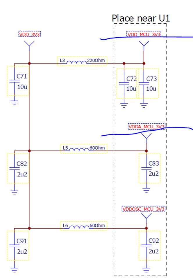
1)      In the datasheet, there are two power pins for F28379: VDDIO is for 3.3V digital I/O power pins while VDDA is for 3.3V analog power pins. In your reference design of ‘F2837x_180controlCARD_R1_3_SCH_02Oct2015.pdf”,  the circuit is like this:


For  VDDIO is connected to VDD_MCU_3V3; for VDDA is connected to VDDA_MCU_3V3. Why do we have to have a VDDA_MCU_3V3 for the analog power pin? Why not connect it directly to VDD_3V3?


I understand the reference design was trying to filter out the noises for VDDA_MCU_3V3, but for most design I saw, there was basically one VDD_3V3 for analog power and one VDD_MCU_3V3 for digital power pin.  Is there a specific reason for adding additional filter to get the VDDA_MCU_3V3?


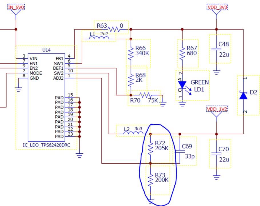
2)      For U14 (IC_LDO_TPS62420DRC), the SW2 output is connected to 205k (R72) and 200k(R73) to get 1.2V. However, based on datasheet, the 1.2V is obtained by Vref * (1+R72/R73) with Vref = 0.6V. After the calculation, the Vout = 1.215V, not the expected 1.2V. If we change R72 to 200k, we will get the 1.2V. Why did the reference design chose R72 as 205k not 200k?


  • Hi Lawrence,

    (1) The inductive bead pi-filters are there to reduce noise - between the analog and digital circuitry, but also to reduce noise from entering the main power supply.  Please note that the true needs for the F2837x's power supplies are shown in the device datasheet and that the inductive bead filters are not required.  A solid statement can be made for doing what you proposed and beads can cause issues if they're not used carefully.  Please note that the "best" power distribution network will often depend on the layout and the EMC requirements for the product being developed.  As a result, the product designer will often be the best at determining what "best" means.


    (2) The datasheet requirement for the device is that the power rails stay within +/-5% of the nominal value during operation [1.14V : 1.26V].  With the buck converter's accuracy and incorporating the resistor tolerance, the worst-case output stays within the valid range.

    Vout = 0.6 * (1+ [205K*1.01] / [200K*0.99]) * 1.01 = 1.24V max

    Load regulation on the buck converter will reduce the 1.215V nominal output to something closer to 1.2V. 

    We put the nominal regulation point slightly over 1.2V for this reason, and also to increase the margin between the nominal voltage and 1.14V.

    As with (1), other valid decisions could be made depending on the system that the C2000 is being utilized in.

    Hopefully this helps!


    Thank you,
    Brett