This thread has been locked.

If you have a related question, please click the "Ask a related question" button in the top right corner. The newly created question will be automatically linked to this question.

Protection circuit for F2802x/3x ADC input pins.

Genius 17295 points

Hello,

I have a question about how to protect ADC input pins for F2802x/3x.


MIN value of Absolute MAX rating for ADC input pins is -0.3V.

To protect these pins, using Schottky diode is one of the option.

But schottky diode has large leakage current and it could cause additional ADC error.


Do we have any other recommendation?


Regards,

Satoshi Obata

  • Hi Satoshi-san,

    Generally in majority applications Clamping Diodes are used.
    You can also go through this TI doc: www.ti.com/.../slaa593.pdf

    Regards,
    Gautam
  • Hi Obata-san,

    If you select a Schottky diode with a Vforward < 0.3V (or otherwise with a very low Vforward) and place it directly at the ADC input, this will ensure that he absolute voltage spec's are met and absolutely no current flows through the internal protection diodes inside the ADC input.  However, as you have seen, this results in a diode with huge leakage, probably more than can be compensated for by increasing the ADC S+H. 

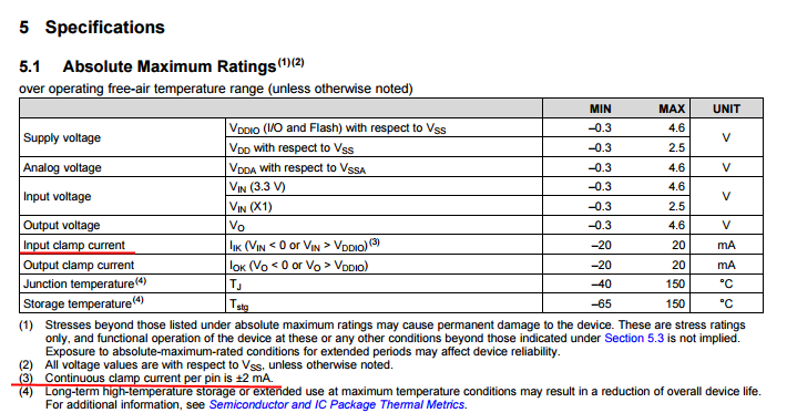
    It is actually ok if the internal protection diodes do some work and conduct some of the current.  We provide a spec' for this as "Input clamp current":


    For the ADC inputs, this is what you really want to control.  If your over/under voltage events are random, then 2mA per pin is a good target.  If your over/under voltage events could all happen at once, then you may need to choose a lower target current to ensure the device total is less than 20mA.  Note that this total also includes clamping events on digital pins.

    One method to control the clamping current would be to add a series R with the ADC input.  On the over-voltage side, if your maximum possible voltage was 5V, the minimum diode voltage was 0.3V, and the minimum VDDA was 3V, then the voltage drop across the resistor would be at most 1.7V.  In this case, an 850ohm R would limit the current to 2mA.  You would still have to compensate for this increased R by increasing the ADC S+H window.

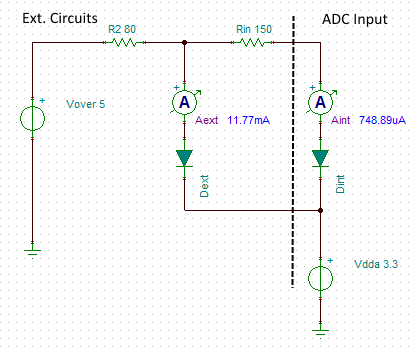
    Now instead of picking a diode with extremely low Vforward, you can actually pick one that is more similar to the internal protection diodes if you use this topology:

    In the simulation above, both the internal and external diodes use the same model.  You can see that by adding "Rin" after the diode, but before the ADC input, most of the current is steered into the external protection diode.  This is because the voltage drop across the internal diode + Rin must be the same as the drop across the external didode. Since the diode current is exponential with voltage, the voltage drop across Rin exponentially decreases the current steered through the internal diode vs. external diode.  R2 is used to limit the current through the external diode.  This still adds some series R, so the S+H window may still need to be slightly increased.

    Using this topology, you can pick a schottky diode (or even a normal silicon diode) with a much less aggressive Vforward spec'.  This will hopefully allow you to control the leakage current to a more manageable level. 

    No matter what protection method you choose, it is imperative to simulate the ADC input settling so that you can pick and appropriate S+h duration.  We provide an input mode of the ADC in the datasheet for this purpose.