This thread has been locked.

If you have a related question, please click the "Ask a related question" button in the top right corner. The newly created question will be automatically linked to this question.

TMS320f2808

Hi,

I have a customer asking about the internal biasing to the ADC and mxc circuits.


“I would be interested in the front end topology for the ADC MUX so I can understand why this biasing occurs. Do you have any analogue block/schematic diagram which would answer my question. I am guessing that the circuitry is forward biasing the mux in some way.

Note that we have this set up on one of our platforms (albeit low accuracy) in this way so I need to know the effect of this biasing and whether it is an issue.”


Thanks,

Jani

  • Hi Jani,

    I am not sure I exactly follow this question.  What is meant by internal biasing here? What effect is the customer seeing or expecting?

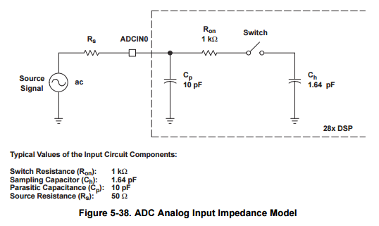
    When designing the signal conditioning circuitry to drive the ADC, we have a switched capacitor ADC input model in most of our device datasheets We unfortunately don't appear to have this model for F2808.  The next best thing is to use the model for F2833x devices (see below).  These devices have the same basic ADC architecture and are built in the same process technology, so this should be a decent proxy for F2808. 

    What you want to do with this model is ensure that the input source can drive Ch from 0 to within 1/4 LSBs of 3.0V during the S+H time.  You can set this up in SPICE, or estimate analytically.  You should assume that Ch and Cp start completely discharged, and you are trying to drive them to the full-scale range (3.0V for this device).  You can also assume that caps start fully charged, and the source can try to discharge them.  

    If you don't get adequate settling, you can:

    -Accept the error.  This error will show up as a random error that sometimes correlates with leftover charge on the S+H capacitor from the previous conversion

    -Increase the S+H duration (by changing the ACQ_PS setting).  This will allow more time for the input to settle (but will slow down the trigger-to-output time, and will reduce the total possible ADC throughput).

    -Reduce the external R and or C.  Note that with an external single-pole LP filter, it is better to have a lower R and higher C for a given pole location.

    -Alternately, you can make the external C right on the pin at least 4096 x 4 x (10pF + 1.64pF) = ~200nF.  This will allow the external capacitor to supply all the charge to get Ch to within 1/4LSBs.  However, this will impose a sample rate limitation on the ADC based on the external source R; the external source still needs to adequately recharge the external C in the time between samples.

  • Hi Devin,

    Thanks for your response earlier but customer is asking for a clarification of what the expected ADC read out value should be under the test condition shown below.


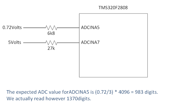
    “Please refer to the drawing below. I think that the error we are seeing is due to the biasing of the internal MUX due to ADCIN7 > 3V. Please also refer to the Note below from document ‘SPRAAP6A’.

  • Hi Jani,

    It looks like your diagram did not show up. Can you try attaching it again?
  • Hi Devin,
    The test conditions are:
    0.72V into ADCINA5 via 6k8 series resistor.
    5V into ADCINA7 via 27k series resistor.
    The ADCLO is connected directly to ground.
    The expected ADC read out value for ADCINA5 is (0.72/3) * 4096 = 983 digits (datasheet page 62)
    Customer is actually reading 1370 digits.
    Why are these different and what is causing it.

    Thanks,
    Jani
  • Hi Jani,

    Applying 5V to the pin violates both the recommended operating conditions and the absolute maximum conditions.  The 27K series resistor will prevent the device from being destroyed by the over-voltage condition, but correct operation of that channel or any other channel on the ADC is not expected until the over-voltage condition is resolved.  

    I believe newer C2000 devices (Piccolo series devices and F2837x devices) are somewhat more resistant to over-voltage on one ADC pin affecting the conversion results on another pin.  

  • Hi Jani,
    We don't have any block diagrams to share but the original hypothesis posed by the customer is correct. The type of switch used for the channel select mux is not protected against the forward bias condition and therefore allows current injection into the other channels when an input exceeds the switch supply (VDDA) by more than a diode drop.

    I'm not sure if the customer is in a position to make HW changes at this point but a couple thoughts to mitigate the issue might be to convert the A7 connection to a voltage divider by adding a resister to ground or add a clamping diode tied to VDDA, though it would need a pretty low turn on voltage to make sure to be below the 0.3V requirement in the DS.

    I hope this satisfies the customer concern,
    Joe
  • Hello Devin,

    On the above post you'd mentioned that,
    =================Alternately, you can make the external C right on the pin at least 4096 x 4 x (10pF + 1.64pF) = ~200nF====================
    Is it the way of selecting external Capacitor at analog input pin for LP filter???
    Then, what should be the external Register value at analog input pin for LP filter???
  • Hi Asim,

    If you want a single-pole passive low-pass filter on the pin, you can go one of two ways:

    -Select R and C to get the cutoff frequency you want. Increase the S+H window to compensate for the increased impedance. In general, you will have to increase the S+H duration less if you select C large and R small for a given cutoff frequency. You won't be able to make the cutoff frequency very low with this strategy (because you can only make the S+H window so long).
    -Select C at least 2^(n+2)*Cadc and R to get the cutoff frequency you want. S+H window can be the minimum as long as R is selected to be low (say 50 ohms or less). You will have to limit the sample rate to prevent drift in the signal due to ADC inrush current. You won't be able to have a very high cutoff frequency (because C is already very large).

    If you can't meet your requirements with these methods, you will need to create an active filter with an op-amp.
  • Hello Devin,

    I'm following your above statement, the result coming at ADCRESULT bit is not correct digital value.
    if changing the ADC pin analog voltage within (0 to 3)V, the ADCRESULT bit always giving a fixed digital value i.e 2047, which's not equal to the analog voltage.

    What'll be the next step to correct the ADCRESULT bit value???