This thread has been locked.

If you have a related question, please click the "Ask a related question" button in the top right corner. The newly created question will be automatically linked to this question.

F2837X trigger a buffer of ADC conversions from ePWM

Other Parts Discussed in Thread: CONTROLSUITE

I wonder if anyone can give me some advice on ADC setup in a F28377S?


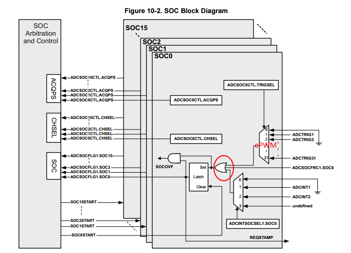
This is what I want to do: Upon an ePWM trigger I want the ADC to start converting two simultaneous channels at the maximum rate for 1000 samples, the resulting 1000 conversions ending up in a buffer in RAM at the end of it all.


The way I’m thinking is this (I describe a single ADC module and will set up both modules the same to get two synchronously sampled inputs):


  1. Set up SOC0 to trigger from the ePWM source

  2. Set up the remaining SOCs to trigger from SOC0 EOC

  3. Also set up an PIE interrupt from the same ePWM source.

  4. Set up DMA to transfer out results 0-7 upon the EOC of SOC7, and results 8 thru 15 upon the EOC of SOC15

  5. In the ISR for the ePWM interrupt change the trigger source of SOC0 to the SOC15 EOC

  6. Set up another PIE interrupt from DMA that will activate after the required 1000 words have been transferred

  7. In the ISR for this, stop the ADC converting and process the data.


Will this work? Is there an easier way to get where I’m going? I’m uncomfortable with the use of the ePWM ISR to reprogram the SOC0 trigger, this needs to be complete before SOC15 EOC, which will be about 4.7µs after the initial ePWM trigger.


Thank you.


John Wilkes.

  • John,

    If you haven't already, I recommend looking at the adc_soc_epwm controlSUITE example:
    controlSUITE\device_support\F2837xS\v210\F2837xS_examples_Cpu1\adc_soc_epwm

    Hope this is a good starting point for your project.

    Elizabeth
  • Hi Elizabeth,


    Thank you for your response. The Control suite examples were, of course, my first port of call, but the example you quote is not applicable to my situation. Indeed none of the examples quite fit the bill or answer my question. Hence my post on this forum.


    If you haven’t already, I invite you the read my requirement carefully. I need the ADC to be converting continuously at maximum sample rate starting with a trigger from the ePWM. The adc_soc_epwm example does one conversion for every ePWM event. The adc_soc_continuous example does have the ADCs converting at maximum rate, but this is started via software and not triggered from the ePWM.


    This has led to my suggestion to use the ePWM to trigger the first conversion and then, in an ISR, swap the trigger source to be continuous. I am nervous that the ISR will not be fast enough to change the ADC trigger before the first set of conversions is done. And I believe I will need to use the DMA engine to do the fast transfer between ADC result registers and RAM.


    Cheers,


    John.

  • Hi John,

    You can actually configure the trigger source to be and OR of both an ADC ISR flag and an ePWM event:

    So I think what you will want to do is start with the continuous conversion example in ControlSUITE.  You can then replace software triggering with ePWM triggering as the means of starting the "ping-pong" of samples.  No need to switch the trigger mode after the first set of conversions. You will need to alter the ADC settings at the end to disable the ADCINT flag triggers to stop the continuous conversion process. 

    It should be possible to collect the samples with the DMA (but I'd suggest getting everything working with CPU based sample collection first).

  • Hi Devin,


    Thank you for your response. That is a good suggestion and I think will get me on my way.


    However, I wonder if I still need to implement an ISR to stop the ePWM trigger? Another one of these could be along as soon as 40µs after the first, well within my 1000 sample window. I don’t want this trigger to upset things (will it? Or will the round robin sequence mean that the conversions will remain on track and in order?).


    Even if I do need this ISR, it has a much longer time to get in and do changes (40µs rather than 4.7µs) so it makes me much less nervous.


    Cheers,


    John.

  • Hi John,

    That's an interesting situation. I do actually think that the round-robin should keep the ADC samples occurring in the correct order even if you asynchronously trigger them again using the ePWM. You will get some ADC overflow flags set in the ADCSOCOVF register, but this won't stop the sampling process and the conversions should still be OK.

    You may want to consider what happens when the DMA ISR is trying to shutdown the sampling process while the ePWM could come in and cause more conversions.

    It may be best to turn off the ePWM SOC events inside the ePWM module just to be safe.
  • Hi Devin,


    OK, I will plan to use an ISR to switch off the ePWM SOC signal. Thanks very much for your help in this matter.


    Cheers,


    John.

  • I have now got my application working and, in the spirit of giving something back to the community (it is, after all, nearly Christmas), I would like to share my final solution in the form of an standalone example that could be used by others who face a similar problem. The example is contained within the attached file which fits into the same structure as the other controlSUITE examples and uses the same header files, library code and linker files. Enjoy!


    /*****************************************************************************/
    /* John Wilkes              AdcContinuousDmaEpwm.c           1 December 2016 */
    /*                                                                           */
    /* This file contains a working example of how to create continuous          */
    /* conversions from the ADC modules, triggered by an EPWM event and read     */
    /* using DMA.                                                                */
    /*                                                                           */
    /* The code is based upon the examples supplied in controlSUITE,             */
    /* specifically the 'adc_soc_continuous', 'adc_soc_epwm' and                 */
    /* 'dma_gsram_transfer' examples. This example fits into the same structure  */
    /* as those and uses the same header files, library code and linker files.   */
    /* The code has been tested on a 28377S launch pad and should also run on a  */
    /* 28379D launch pad with no changes.                                        */
    /*                                                                           */
    /* The specific problem solved is this: Upon an ePWM event, two ADC channels */
    /* (A3 and B3) are converted simultaneously at the maximum sample rate for   */
    /* 1024 samples. The resulting data end up in RAM at the end.                */
    /*                                                                           */
    /* The trigger event used is the timer equals zero event from EPWM module 2. */
    /* This event is also brought out to an IO pin so that it can be monitored   */
    /* externally if required. The output could also be used as a source for one */
    /* of the ADC inputs (careful: need to pot down the voltage from the ePWM    */
    /* pin as this exceeds the maximum ADC input voltage). EPWM module 2 is used */
    /* because it is accessible on both target launch pads. Which, by the way,   */
    /* is also the reason ADC channels A3 and B3 where chosen.                   */
    /*                                                                           */
    /* DMA is used to move data from the ADC result registers and into RAM.      */
    /* GSRAM is used for this as LSRAM cannot be accessed by the DMA engine. A   */
    /* DMA channel is required for each ADC channel.                             */
    /*****************************************************************************/
    
    /***********/
    /* INCLUDE */
    /***********/
    #include "F28x_Project.h"
    
    /**********/
    /* LABELS */
    /**********/
    
    /* Extensions to the TI supplied register defines: Although the unioned bit  */
    /* field approach used in the TI header files is useful, it can be           */
    /* inefficient in some cases. Particularly when writing to a register that   */
    /* contains a combination of read only and/or write-one-to-clear bits. The   */
    /* bit field approach will result in the compiler generating a read,         */
    /* followed by a bitwise OR and then, finally, a write. Since writing zero   */
    /* to bits in this kind of register has no effect, it is quicker to do a     */
    /* write to the whole register with relevant bits set. Hence I have defined  */
    /* labels for the various bits I have used in the program. This is not an    */
    /* complete list, only the registers I have used.                            */
    #define DMA_RUN 0x1
    #define DMA_HALT 0x2
    #define DMA_SOFTRESET 0x4
    #define DMA_PERINTFRC 0x8
    #define DMA_PERINTCLR 0x10
    
    #define ADC_INT1CLR 0x1
    #define ADC_INT2CLR 0x2
    #define ADC_INT3CLR 0x4
    #define ADC_INT4CLR 0x8
    
    #define ADC_TRIGSEL_EPWM1_SOCA 0x5
    #define ADC_TRIGSEL_EPWM2_SOCA 0x7
    #define ADC_TRIGSEL_EPWM7_SOCA 0x11
    
    #define EPWM_ETINTCLR 0x1
    #define EPWM_ETSOCACLR 0x4
    #define EPWM_ETSOCBCLR 0x8
    
    /* Size of results buffer must be a multiple of sixteen */
    #define RESULTS_BUFFER_SIZE 1024
    
    /***********************/
    /* FUNCTION PROTOTYPES */
    /***********************/
    __interrupt void adcIsr(void);
    __interrupt void dmaIsr(void);
    void ePwmSetup (volatile struct EPWM_REGS * pwmRegs);
    void configureADC(void);
    void setupADCContinuous(volatile struct ADC_REGS * adcRegs, Uint16 channel);
    void dmaInit();
    
    /***********/
    /* GLOBALS */
    /***********/
    
    /* The results buffer must be located in GSRAM as LSRAM is not accessible by */
    /* the DMA engine                                                            */
    #pragma DATA_SECTION(adcData0, "ramgs0");
    #pragma DATA_SECTION(adcData1, "ramgs0");
    Uint16 adcData0[RESULTS_BUFFER_SIZE];
    Uint16 adcData1[RESULTS_BUFFER_SIZE];
    
    /********/
    /* CODE */
    /********/
    
    /*****************/
    /* PROGRAM ENTRY */
    /*****************/
    void main(void)
    {
    	/**************************************/
    	/* STEP 1 - INITIALISE SYSTEM CONTROL */
    	/**************************************/
    
    	/* PLL, WatchDog, enable Peripheral Clocks. This example function is */
    	/* found in the F2837xX_SysCtrl.c file.                              */
    	InitSysCtrl();
    
        /* ALSO: Change the LSPCLK divider to /1 so that LSPCLK is 200MHz */
        EALLOW;
        ClkCfgRegs.LOSPCP.bit.LSPCLKDIV = 0;
        EDIS;
    
    
        /*****************/
        /* STEP 2 - GPIO */
        /*****************/
    
        /* Expose ePWM 2A on GPIO pin 2. The GPIO setup functions are found in */
        /* the F2837xX_Gpio.c file                                             */
    	GPIO_SetupPinMux(2, GPIO_MUX_CPU1, 1);
    
        /* Though not needed externally, we set up GPIO0 as an output and drive  */
    	/* it low. This pin drives the EPWMxSYNC inputs to the EPWM modules and, */
    	/* as we will enable the initialisation of the ET counter (so we can     */
    	/* manually reset it), we do not want the SYNCI signal to also reset it  */
    	/* - hence connecting SYNCI to a permanent low. If the application needs */
    	/* to use the GPIO0 pin, then the SYNCI signal can be derived from       */
    	/* another (unused) pin using the xbar registers.                        */
    	GPIO_SetupPinMux(0, GPIO_MUX_CPU1, 0);
    	GPIO_SetupPinOptions(0, GPIO_OUTPUT, 0);
    	GPIO_WritePin(0, 0);
    
    	/***********************/
    	/* STEP 3 - INTERRUPTS */
    	/***********************/
    
    	/* Clear all interrupts and initialise PIE vector table */
    
    	/* Disable CPU interrupts */
        DINT;
    
    	/* Initialise the PIE control registers to their default state. The    */
        /* default state is all PIE interrupts disabled and flags are cleared. */
    	/* This function is found in the F2837xX_PieCtrl.c file.               */
        InitPieCtrl();
    
        /* Disable CPU interrupts and clear all CPU interrupt flags */
        IER = 0x0000;
        IFR = 0x0000;
    
    	/* Initialise the PIE vector table with pointers to the shell Interrupt */
        /* Service Routines (ISR). This will populate the entire table, even if */
        /* the interrupt is not used in this example. This is useful for debug  */
        /* purposes. The shell ISR routines are found in F2837xX_DefaultIsr.c.  */
        /* This function is found in F2837xX_PieVect.c.                         */
        InitPieVectTable();
    
        /* Now set ISRs used by this example */
        EALLOW;
    
        /* ISR for ADCA INT1 - occurs after first conversion */
        PieVectTable.ADCA1_INT = &adcIsr;
    
        /* ISR for DMA ch1 - occurs when DMA transfer is complete */
        PieVectTable.DMA_CH1_INT = &dmaIsr;
    
        EDIS;
    
        /* Enable specific CPU interrupts: INT1 for ADCs and INT7 for DMA */
    	IER |= M_INT1;
    	IER |= M_INT7;
    
    	/* Enable specific PIE interrupts */
    
    	/* ADCA INT1: Group 1, interrupt 1 */
    	PieCtrlRegs.PIEIER1.bit.INTx1 = 1;
    
    	/* DMA interrupt: Group 7, interrupt 1 */
    	PieCtrlRegs.PIEIER7.bit.INTx1 = 1;
    
    	/***********************************/
    	/* STEP 4 - EXAMPLE SPECIFIC SETUP */
    	/***********************************/
    
    	/**********/
    	/**********/
    	/** EPWM **/
    	/**********/
    	/**********/
    
    	/* Stop the EPWM clock */
    	EALLOW;
    	CpuSysRegs.PCLKCR0.bit.TBCLKSYNC = 0;
    	EDIS;
    
    	/* Call the set up function for ePWM 2. Function is located later in */
    	/* this file                                                         */
    	ePwmSetup(&EPwm2Regs);
    
    	/* Start the EPWM clock */
    	EALLOW;
    	CpuSysRegs.PCLKCR0.bit.TBCLKSYNC = 1;
    	EDIS;
    
    	/*********/
    	/*********/
    	/** ADC **/
    	/*********/
    	/*********/
    
    	/* ADC setup functions are located later in this file. Using channels A3 */
    	/* and B3 as these are accessible on both 28377S and 28379D launch pads  */
    	configureADC();
    	setupADCContinuous(&AdcaRegs, 3); /* A3 */
    	setupADCContinuous(&AdcbRegs, 3); /* B3 */
    
    	/*********/
    	/*********/
    	/** DMA **/
    	/*********/
    	/*********/
    
    	/* DMA setup function is located later in this file */
    	dmaInit();
    
    	/*************************************/
    	/* STEP 5 - ENABLE GLOBAL INTERRUPTS */
    	/*************************************/
    	EINT;  /* Enable Global interrupt INTM           */
    	ERTM;  /* Enable Global real time interrupt DBGM */
    
    	/*--------------------------- SETUP COMPLETE ----------------------------*/
    
    	/* That's the set up done - now we do a grab of the data. This block of */
    	/* code could be re-called as part of the application to grab more data */
    
    	/* Some of the registers here are EALLOW, so just set it for the */
    	/* duration                                                      */
    	EALLOW;
    
    	/* Reset the sequence by clearing all pending interrupt flags */
    	DmaRegs.CH1.CONTROL.all = DMA_PERINTCLR;
    	DmaRegs.CH2.CONTROL.all = DMA_PERINTCLR;
    	AdcaRegs.ADCINTFLGCLR.all =	ADC_INT1CLR | ADC_INT2CLR;
    	AdcbRegs.ADCINTFLGCLR.all =	ADC_INT1CLR | ADC_INT2CLR;
    	EPwm2Regs.ETCNTINITCTL.bit.SOCAINITFRC = 1;
    	EPwm2Regs.ETCLR.all = EPWM_ETSOCACLR;
        PieCtrlRegs.PIEIFR7.bit.INTx1 = 0;
        PieCtrlRegs.PIEIFR1.bit.INTx1 = 0;
    
    	/* Enable continuous operation by setting the last SOC to re-trigger the */
        /* first                                                                 */
    	AdcaRegs.ADCINTSOCSEL1.bit.SOC0 = 2;
    	AdcbRegs.ADCINTSOCSEL1.bit.SOC0 = 2;
    
    	/* Enable the interrupt from the very first conversion: the ISR for this */
    	/* (adcIsr) will remove the ePWM trigger and disable itself.             */
    	PieCtrlRegs.PIEIER1.bit.INTx1 = 1;
    
        /* Start DMA - note not using the library function to do this: it does  */
    	/* an EDIS!                                                             */
        DmaRegs.CH1.CONTROL.all = DMA_RUN;
        DmaRegs.CH2.CONTROL.all = DMA_RUN;
    
        /* Finally, enable the SOCA trigger from EPWM. This will kick off */
        /* conversions at the next ePWM event                             */
        EPwm2Regs.ETSEL.bit.SOCAEN = 1;
    
    	/* The rest of the functionality of the ADC grab is done in the DMA and */
    	/* ADC ISRs: adcIsr and dmaIsr. Alternatively: it can be done without   */
    	/* using interrupts by the commented out code below. This reduces the   */
    	/* risk of nasty interrupt timing issues, but will waste CPU time that  */
    	/* may be better spent elsewhere. For 1024 samples, the while loops     */
    	/* below will stall for about 300us                                     */
    
    //	/* Wait for first conversion to complete */
    //	while(0 == AdcaRegs.ADCINTFLG.bit.ADCINT1) ;
    //
    //	/* Remove EPWM trigger */
    //	EPwm2Regs.ETSEL.bit.SOCAEN = 0;
    //
    //	/* Wait for transfer complete */
    //	while(0 == PieCtrlRegs.PIEIFR7.bit.INTx1) ;
    //
    //	/* Stop the ADC by removing the trigger for SOC0 */
    //	AdcaRegs.ADCINTSOCSEL1.bit.SOC0 = 0;
    //	AdcbRegs.ADCINTSOCSEL1.bit.SOC0 = 0;
    
        EDIS;
    
    	/* Stall */
    	for (;;) {
    		asm(" NOP");
    	}
    
    }
    
    /********************************/
    /********************************/
    /** INTERRUPT SERVICE ROUTINES **/
    /********************************/
    /********************************/
    
    /****************************************************************************/
    /* adcIsr                                                               ISR */
    /* This is called after the very first conversion and will disable the EPWM */
    /* SOC to avoid re-triggering problems.                                     */
    /****************************************************************************/
    #pragma CODE_SECTION(adcIsr, ".TI.ramfunc");
    __interrupt void adcIsr(void)
    {
    	/* Remove EPWM trigger */
        EPwm2Regs.ETSEL.bit.SOCAEN = 0;
    
    	/* Disable this interrupt from happening again */
    	PieCtrlRegs.PIEIER1.bit.INTx1 = 0;
    
    	/* Acknowledge */
    	PieCtrlRegs.PIEACK.all = PIEACK_GROUP1;
    }
    
    /**********************************************************************/
    /* dmaIsr                                                         ISR */
    /* This is called at the end of the DMA transfer, the conversions are */
    /* stopped by removing the trigger of the first SOC from the last.    */
    /**********************************************************************/
    #pragma CODE_SECTION(dmaIsr, ".TI.ramfunc");
    __interrupt void dmaIsr(void)
    {
    	/* Stop the ADC by removing the trigger for SOC0 */
    	EALLOW;
    	AdcaRegs.ADCINTSOCSEL1.bit.SOC0 = 0;
    	AdcbRegs.ADCINTSOCSEL1.bit.SOC0 = 0;
    	EDIS;
    
    	/* Acknowledge */
    	PieCtrlRegs.PIEACK.all = PIEACK_GROUP7;
    }
    
    /********************************/
    /********************************/
    /** PERIPHERAL SETUP FUNCTIONS **/
    /********************************/
    /********************************/
    
    /****************************************************************************/
    /* ePwmSetup                                                       FUNCTION */
    /* Sets up the specified ePWM module so that the A output has a period of   */
    /* 40us with a 50% duty. The SOCA signal is coincident with the rising edge */
    /* of this.                                                                 */
    /****************************************************************************/
    void ePwmSetup (volatile struct EPWM_REGS * pwmRegs)
    {
    	/* Make the timer count up with a period of 40us */
    	pwmRegs->TBCTL.all = 0x0000;
    	pwmRegs->TBPRD = 4000;
    
    	/* Set the A output on zero and reset on CMPA */
    	pwmRegs->AQCTLA.bit.ZRO = AQ_SET;
    	pwmRegs->AQCTLA.bit.CAU = AQ_CLEAR;
    
    	/* Set CMPA to 20us to get a 50% duty */
    	pwmRegs->CMPA.bit.CMPA = 2000;
    
    	/* Start ADC when timer equals zero (note: don't enable yet) */
    	pwmRegs->ETSEL.bit.SOCASEL = ET_CTR_ZERO;
    	pwmRegs->ETPS.bit.SOCAPRD =  ET_1ST;
    
    	/* Enable initialisation of the SOCA event counter - since we are     */
    	/* disabling the ETSEL.SOCAEN bit, we need a way to reset the SOCACNT */
    	/* Hence, enable the counter initialise control                       */
        pwmRegs->ETCNTINITCTL.bit.SOCAINITEN = 1;
    }
    
    /**************************************************************************/
    /* configureADC                                                  FUNCTION */
    /* Write ADC configurations and power up the ADC for both ADC A and ADC B */
    /**************************************************************************/
    void configureADC(void)
    {
        EALLOW;
    
        /* Set pre-scale for 50MHz operation (divide SYSCLK by 4) */
        AdcaRegs.ADCCTL2.bit.PRESCALE = 6;
        AdcbRegs.ADCCTL2.bit.PRESCALE = 6;
    
        /* Set Mode */
        AdcSetMode(ADC_ADCA, ADC_RESOLUTION_12BIT, ADC_SIGNALMODE_SINGLE);
        AdcSetMode(ADC_ADCB, ADC_RESOLUTION_12BIT, ADC_SIGNALMODE_SINGLE);
    
        /* Late interrupt */
        AdcaRegs.ADCCTL1.bit.INTPULSEPOS = 1;
        AdcbRegs.ADCCTL1.bit.INTPULSEPOS = 1;
    
        /* Power up */
        AdcaRegs.ADCCTL1.bit.ADCPWDNZ = 1;
        AdcbRegs.ADCCTL1.bit.ADCPWDNZ = 1;
    
        /* Delay for 1ms to allow ADC time to power up */
        DELAY_US(1000);
    
        EDIS;
    }
    
    /****************************************************************************/
    /* setupADCContinuous                                              FUNCTION */
    /* Set up all the SOCs of the specified ADC module to convert the specified */
    /* channel at maximum rate (i.e. minimum sample window). SOC0 will trigger  */
    /* from an EPWM SOC and all other SOCs trigger from the EOC of SOC0 - the   */
    /* round robin mechanism ensures they convert in order. Prior to enabling   */
    /* the trigger, SOC0 should be set to also trigger from SOC15 EOC (INT2)    */
    /* which will cause continuous converting until this is removed.            */
    /****************************************************************************/
    void setupADCContinuous(volatile struct ADC_REGS * adcRegs, Uint16 channel)
    {
    	/* Use minimum acquisition window for 12 bit resolution */
    	/* Sample window is acqps + 1 SYSCLK cycles             */
        Uint16 acqps = 14;
    
        /* Set all SOCs to convert the same channel (wot no loop?) */
        EALLOW;
        adcRegs->ADCSOC0CTL.bit.CHSEL  = channel;
        adcRegs->ADCSOC1CTL.bit.CHSEL  = channel;
        adcRegs->ADCSOC2CTL.bit.CHSEL  = channel;
        adcRegs->ADCSOC3CTL.bit.CHSEL  = channel;
        adcRegs->ADCSOC4CTL.bit.CHSEL  = channel;
        adcRegs->ADCSOC5CTL.bit.CHSEL  = channel;
        adcRegs->ADCSOC6CTL.bit.CHSEL  = channel;
        adcRegs->ADCSOC7CTL.bit.CHSEL  = channel;
        adcRegs->ADCSOC8CTL.bit.CHSEL  = channel;
        adcRegs->ADCSOC9CTL.bit.CHSEL  = channel;
        adcRegs->ADCSOC10CTL.bit.CHSEL = channel;
        adcRegs->ADCSOC11CTL.bit.CHSEL = channel;
        adcRegs->ADCSOC12CTL.bit.CHSEL = channel;
        adcRegs->ADCSOC13CTL.bit.CHSEL = channel;
        adcRegs->ADCSOC14CTL.bit.CHSEL = channel;
        adcRegs->ADCSOC15CTL.bit.CHSEL = channel;
    
        /* Set all SOCs to minimum acquisition window */
        adcRegs->ADCSOC0CTL.bit.ACQPS  = acqps;
        adcRegs->ADCSOC1CTL.bit.ACQPS  = acqps;
        adcRegs->ADCSOC2CTL.bit.ACQPS  = acqps;
        adcRegs->ADCSOC3CTL.bit.ACQPS  = acqps;
        adcRegs->ADCSOC4CTL.bit.ACQPS  = acqps;
        adcRegs->ADCSOC5CTL.bit.ACQPS  = acqps;
        adcRegs->ADCSOC6CTL.bit.ACQPS  = acqps;
        adcRegs->ADCSOC7CTL.bit.ACQPS  = acqps;
        adcRegs->ADCSOC8CTL.bit.ACQPS  = acqps;
        adcRegs->ADCSOC9CTL.bit.ACQPS  = acqps;
        adcRegs->ADCSOC10CTL.bit.ACQPS = acqps;
        adcRegs->ADCSOC11CTL.bit.ACQPS = acqps;
        adcRegs->ADCSOC12CTL.bit.ACQPS = acqps;
        adcRegs->ADCSOC13CTL.bit.ACQPS = acqps;
        adcRegs->ADCSOC14CTL.bit.ACQPS = acqps;
        adcRegs->ADCSOC15CTL.bit.ACQPS = acqps;
    
        /* Trigger SCO0 from EPWM */
        adcRegs->ADCSOC0CTL.bit.TRIGSEL = ADC_TRIGSEL_EPWM2_SOCA;
    
        /* Trigger all other SOCs from INT1 (EOC on SOC0) */
        adcRegs->ADCINTSOCSEL1.bit.SOC1 = 1;
        adcRegs->ADCINTSOCSEL1.bit.SOC2 = 1;
        adcRegs->ADCINTSOCSEL1.bit.SOC3 = 1;
        adcRegs->ADCINTSOCSEL1.bit.SOC4 = 1;
        adcRegs->ADCINTSOCSEL1.bit.SOC5 = 1;
        adcRegs->ADCINTSOCSEL1.bit.SOC6 = 1;
        adcRegs->ADCINTSOCSEL1.bit.SOC7 = 1;
        adcRegs->ADCINTSOCSEL2.bit.SOC8 = 1;
        adcRegs->ADCINTSOCSEL2.bit.SOC9 = 1;
        adcRegs->ADCINTSOCSEL2.bit.SOC10 = 1;
        adcRegs->ADCINTSOCSEL2.bit.SOC11 = 1;
        adcRegs->ADCINTSOCSEL2.bit.SOC12 = 1;
        adcRegs->ADCINTSOCSEL2.bit.SOC13 = 1;
        adcRegs->ADCINTSOCSEL2.bit.SOC14 = 1;
        adcRegs->ADCINTSOCSEL2.bit.SOC15 = 1;
    
        /* Enable interrupts 1 and 2 */
        adcRegs->ADCINTSEL1N2.bit.INT1E = 1; // Enable INT1 flag
        adcRegs->ADCINTSEL1N2.bit.INT2E = 1; // Enable INT2 flag
        adcRegs->ADCINTSEL3N4.bit.INT3E = 0;
        adcRegs->ADCINTSEL3N4.bit.INT4E = 0;
    
        /* Enable continuous mode on the active interrupts - otherwise           */
        /* conversions will stall waiting for acknowledgement that never happens */
        adcRegs->ADCINTSEL1N2.bit.INT1CONT = 1;
        adcRegs->ADCINTSEL1N2.bit.INT2CONT = 1;
    
        /* Set source of interrupts */
        adcRegs->ADCINTSEL1N2.bit.INT1SEL = 0;  /* end of SOC0  */
        adcRegs->ADCINTSEL1N2.bit.INT2SEL = 15; /* end of SOC15 */
    
        EDIS;
    }
    
    /*****************************************************************************/
    /* dmaInit                                                          FUNCTION */
    /* This sets up the DMA to scoop up data from the ADC result registers and   */
    /* throw it into the result arrays in RAM. Each burst is triggered from the  */
    /* EOC of ADC SOC15 and will move all sixteen results into RAM. The bursts   */
    /* repeat until the results arrays are full. The setup functions used here   */
    /* are found in F2837xX_DMA.c.                                               */
    /*                                                                           */
    /* NOTE ABOUT 16 BIT and 32 BIT TRANSFER SIZES:                              */
    /* This is not documented at all well (indeed, at all as far as I can see),  */
    /* The following is the result of trial and error and observations on a real */
    /* device:                                                                   */
    /*                                                                           */
    /* When using 16 bit transfer size:                                          */
    /*  * The burst size is one less than the number of 16 bit words that need   */
    /*    to be transferred in the burst. E.g. for 8 16 bit words the burst size */
    /*    needs to be set to 7.                                                  */
    /*  * The burst step sizes (src and dst) need to reflect the number to add   */
    /*    to the address pointer after each word is transferred. E.g If the      */
    /*    words transferred in a burst are from contiguous addresses, the step   */
    /*    size is 1.                                                             */
    /*  * At the end of a burst, the address pointer is still pointing at the    */
    /*    last word that was transferred. I.e. the last burst step has NOT been  */
    /*    applied. The transfer step needs to take this into account. E.g. If    */
    /*    the burst was 8 words long (i.e. burst size = 7) and the next burst    */
    /*    needs to go back and transfer the same block of memory again, the      */
    /*    transfer step should be -7. If the next burst needs to continue on     */
    /*    from the previous one, then the transfer step size should be 1.        */
    /*                                                                           */
    /* This is subtly different to when using 32 bit transfer size:              */
    /*  * The burst size is the number of 16 bit words that need to be           */
    /*    transferred - this is the one thing that the documentation is clear    */
    /*    about, but notice that it is not less one for 32 bit transfers. E.g.   */
    /*    for 4 32 bit words the burst size needs to be set to 8.                */
    /*  * The burst step sizes (src and dst) need to reflect the number to add   */
    /*    to the address pointer after each word is transferred. This is the     */
    /*    same rule as in 16 bit transfer size, but remember each 32 bit         */
    /*    transfer consumes 2 pointer addresses. E.g If the words transferred in */
    /*    a burst are from contiguous addresses, the step size is 2.             */
    /*  * At the end of a burst, the address pointer is pointing at the next     */
    /*    word to transfer. I.e. the last burst step HAS been applied. The       */
    /*    transfer step needs to take this into account. E.g. If the burst was 4 */
    /*    32 words long (i.e. burst size = 8) and the next burst needs to go     */
    /*    back and transfer the same block of memory again, the transfer step    */
    /*    should be -8. If the next burst needs to continue on from the previous */
    /*    one, then the transfer step size should be 0.                          */
    /*                                                                           */
    /* In both cases the transfer size is one less than the number of bursts in  */
    /* the transfer. I.e. if there are to be 64 bursts, the transfer size should */
    /* be 63.                                                                    */
    /*                                                                           */
    /* Haven't investigated the effect on wrap operation as I haven't had cause  */
    /* to use it!                                                                */
    /*****************************************************************************/
    void dmaInit()
    {
        /* Initialise DMA */
        DMAInitialize();
    
        /* DMA set up for first ADC */
        DMACH1AddrConfig(adcData0, &AdcaResultRegs.ADCRESULT0);
        /* This commented out bit is for 16 bit transfers - see above */
        //DMACH1BurstConfig(15, 1, 1);
        //DMACH1TransferConfig((RESULTS_BUFFER_SIZE>>4)-1,-15,1);
        DMACH1BurstConfig(16, 2, 2);
        DMACH1TransferConfig((RESULTS_BUFFER_SIZE>>4)-1, -16, 0);
        DMACH1ModeConfig(
    		DMA_ADCAINT2,
    		PERINT_ENABLE,
    		ONESHOT_DISABLE,
    		CONT_DISABLE,
    		SYNC_DISABLE,
    		SYNC_SRC,
    		OVRFLOW_DISABLE,
    		//SIXTEEN_BIT,
    		THIRTYTWO_BIT,
    		CHINT_END,
    		CHINT_ENABLE
    	);
    
        /* DMA set up for second ADC */
        DMACH2AddrConfig(adcData1, &AdcbResultRegs.ADCRESULT0);
        /* This commented out bit is for 16 bit transfers - see above */
        //DMACH2BurstConfig(15, 1, 1);
        //DMACH2TransferConfig((RESULTS_BUFFER_SIZE>>4)-1,-15,1);
        DMACH2BurstConfig(16, 2, 2);
        DMACH2TransferConfig((RESULTS_BUFFER_SIZE>>4)-1, -16, 0);
        DMACH2ModeConfig(
    		DMA_ADCAINT2,
    		PERINT_ENABLE,
    		ONESHOT_DISABLE,
    		CONT_DISABLE,
    		SYNC_DISABLE,
    		SYNC_SRC,
    		OVRFLOW_DISABLE,
    		//SIXTEEN_BIT,
    		THIRTYTWO_BIT,
    		CHINT_END,
    		CHINT_DISABLE
    	);
    }


    A couple of issues that I came across while doing this:


    1. In the adc_soc_continuous example in controlSUITE, there is an EALLOW/EDIS pair missing from around the code that sets the ADCINT enable flags.
    2. The required setting for burst size and transfer step in the DMA engine subtly changes depending upon whether you use 16 or 32 bit transfers. I cannot find a description of this anywhere, so had to work it out by observation: my findings are contained as a comment in the example file.
    3. There is an error in the LAUNCHXL-F28377S Overview User's Guide (sprui25a). Table 4 shows J8-80/79 to be GPIO2/3 and EPWM1A/B. Should be EPWM2A/B.
    4. In the Technical Reference Manuals for the 2837xS/D. The description of the ADCBSYCHN field of the ADCCTRL1 register refers to ADC “channels”. I think the field actually reports SOC number. It is also confusing that it only specifies possible values up to 11 (Bh), when there are 16 SOCs (and, for that matter, 16 channels).

    Cheers,

    John

  • Hi John,

    Thanks for putting this together! We'll work on integrating this example into ControlSUITE as well as addressing the issues you have found in the documentation!
  • Hey John,

    That's very kind of you to report bugs as well as the solutions. That's exactly how a community grows GAIN & SHARE KNOWLEDGE!

    Regards,
    Gautam