

Hi;
I am new with PICOLLO and Embedded coding. I am using TMS320F28027PT, using CH4(AIO4) to read an analog input and I need to use a 12 bit DAC MCP4921 that
should output the analog signal read by ADC.
I am using SPI 3 wire connection. Active low CS of the DAC is connected to the GPIO34/comp2out, GPIO16 is connected to DAC's SDI(Serial Data in)-input, and
DAC's SCk is connected to GPIO18 as an SPICLK.
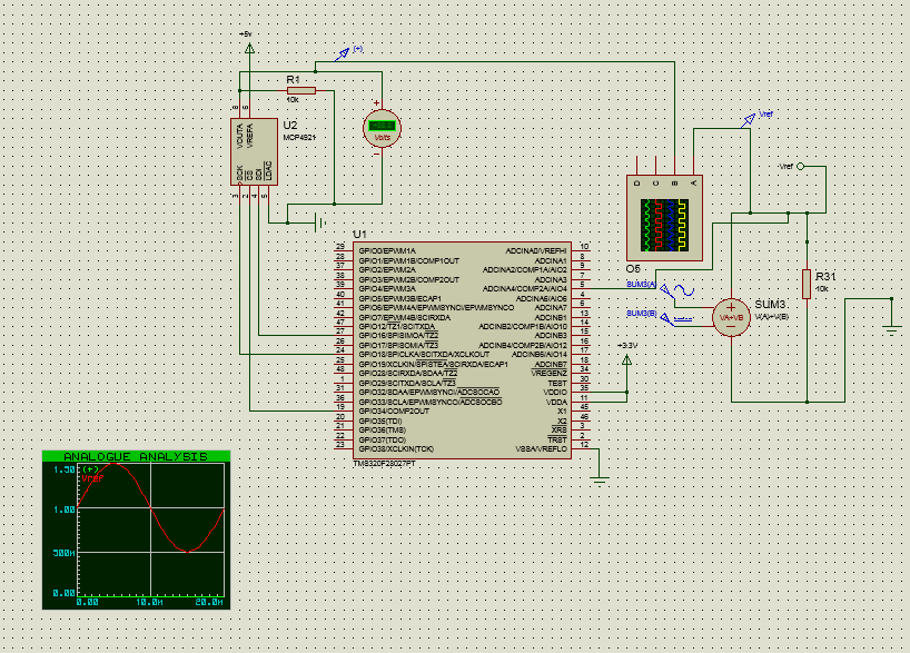
MY ACINA4/AIO4 is not active (grey)should be red in simulation, and the DAC Output is zero, looks like as if it does not read the ADC channel 4, obviously I
am doing smth wrong with either ADC or SPI Which I cannot fix. IF you Can Please help.I am Using Proteus to simulate all this. the code compiles with
no error.
Here I paste my Code and Schematic
Thanks,
Ahmad
*****************************************************************************************
#include "F2802x_Device.h" // Headerfile Include File
#include "f2802x_examples.h"
#define ADC_usDELAY 1000L
void InitAdc(void)
{
extern void DSP28x_usDelay(Uint32 Count);
EALLOW;
SysCtrlRegs.PCLKCR0.bit.ADCENCLK = 1;
(*Device_cal)();
EDIS;
EALLOW;
AdcRegs.ADCCTL1.bit.ADCBGPWD = 1; // Power ADC BG
AdcRegs.ADCCTL1.bit.ADCREFPWD = 1; // Power reference
AdcRegs.ADCCTL1.bit.ADCPWDN = 1; // Power ADC
AdcRegs.ADCCTL1.bit.ADCENABLE = 1; // Enable ADC
AdcRegs.ADCCTL1.bit.ADCREFSEL = 0; // Select internal BG
DELAY_US(ADC_usDELAY); // Delay before converting ADC channels
AdcRegs.ADCSOC0CTL.bit.CHSEL = 4; // Convert channel ADCINA4 (ch4); set SOC0 channel select to ADCINA4
AdcRegs.ADCSOC0CTL.bit.ACQPS = 6; // Acquisition window set to (6+1)=7 cycles
GpioCtrlRegs.AIOMUX1.bit.AIO4 = 2; // Configure AIO4 for A4 (analog input) operation
AdcRegs.INTSEL1N2.bit.INT1E = 1; // Enabled ADCINT1
AdcRegs.INTSEL1N2.bit.INT1CONT = 0;
AdcRegs.ADCCTL1.bit.INTPULSEPOS = 1; //ADCINTs trigger at end of conversion
AdcRegs.INTSEL1N2.bit.INT1SEL = 6; // //EOC6 triggers ADCINT1
AdcRegs.ADCINTSOCSEL1.bit.SOC0 = 1; //ADCINT1 starts SOC0
EDIS ;
DELAY_US(ADC_usDELAY); // Delay before converting ADC channels
}
void spi_init()
{
SpiaRegs.SPICCR.all =0x000F; // Reset on, rising edge, 16-bit char bits
SpiaRegs.SPICTL.all =0x0006; // Enable master mode, normal phase,
// enable talk, and SPI int disabled.
SpiaRegs.SPIBRR =0x007F;
SpiaRegs.SPICCR.all =0x009F; // Relinquish SPI from Reset
SpiaRegs.SPIPRI.bit.FREE = 1; // Set so breakpoints don't disturb xmission
}
void spi_xmit(Uint16 a) //before it was Uint16 a
{
SpiaRegs.SPITXBUF=a;
}
void spi_fifo_init()
{
// Initialize SPI FIFO registers
SpiaRegs.SPIFFTX.all=0xE040;
SpiaRegs.SPIFFRX.all=0x2044;
SpiaRegs.SPIFFCT.all=0x0;
}
void InitGpio(void)
{
EALLOW;
GpioCtrlRegs.GPAPUD.bit.GPIO16 = 0; // Enable pull-up on GPIO16 (SPISIMOA)
GpioCtrlRegs.GPAPUD.bit.GPIO17 = 0; // Enable pull-up on GPIO17 (SPISOMIA)
GpioCtrlRegs.GPAPUD.bit.GPIO18 = 0; // Enable pull-up on GPIO18 (SPICLKA)
GpioCtrlRegs.GPAPUD.bit.GPIO19 = 0; // Enable pull-up on GPIO19 (SPISTEA)
GpioCtrlRegs.GPAQSEL2.bit.GPIO16 = 3; // Asynch input GPIO16 (SPISIMOA)
GpioCtrlRegs.GPAQSEL2.bit.GPIO17 = 3; // Asynch input GPIO17 (SPISOMIA)
GpioCtrlRegs.GPAQSEL2.bit.GPIO18 = 3; // Asynch input GPIO18 (SPICLKA)
GpioCtrlRegs.GPAQSEL2.bit.GPIO19 = 3; // Asynch input GPIO19 (SPISTEA)
GpioCtrlRegs.GPAMUX2.bit.GPIO16 = 1; // Configure GPIO16 as SPISIMOA
GpioCtrlRegs.GPAMUX2.bit.GPIO17 = 1; // Configure GPIO17 as SPISOMIA
GpioCtrlRegs.GPAMUX2.bit.GPIO18 = 1; // Configure GPIO18 as SPICLKA
GpioCtrlRegs.GPAMUX2.bit.GPIO19 = 1; // Configure GPIO19 as SPISTEA
GpioCtrlRegs.GPADIR.bit. GPIO17 = 0;// GPIO17 is input
GpioCtrlRegs.GPADIR.bit.GPIO16 = 1;
GpioCtrlRegs.GPADIR.bit.GPIO18 = 1;
GpioCtrlRegs.GPADIR.bit.GPIO19 = 1;
GpioCtrlRegs.GPBMUX1.bit.GPIO34 = 0; // 0=GPIO, 1=COMP2OUT, 2=EMU1, 3=Resv
GpioCtrlRegs.GPBDIR.bit.GPIO34 = 1; // 1=OUTput, 0=INput
GpioDataRegs.GPBSET.bit.GPIO34 = 1;
EDIS;
}
void DAC(unsigned int value )
{
EALLOW;
char tem;
tem = (value>>8) & 0x0F ; //store bits 8:11 in "tem"
tem |= 0x30; // DAc setting for gain
GpioDataRegs.GPBDAT.bit.GPIO34 = 0; //ChipSelect = 0; for Enable DAC
spi_xmit(tem);// write to DAC
while(SpiaRegs.SPIFFRX.bit.RXFFST !=1) { }
tem = value ; //send low byte
spi_xmit(tem);// write to DAC
while(SpiaRegs.SPIFFRX.bit.RXFFST !=1) { }
GpioDataRegs.GPBDAT.bit.GPIO34 =1; //ChipSelect = 1; //Disable DAC
}
void main() {
#ifdef _FLASH
memcpy(&RamfuncsRunStart, &RamfuncsLoadStart, (size_t)&RamfuncsLoadSize);
#endif
InitSysCtrl();
EALLOW;
GpioCtrlRegs.GPAMUX2.bit.GPIO18 = 3; //enable XCLOCKOUT through GPIO mux
SysCtrlRegs.XCLK.bit.XCLKOUTDIV = 2; //XCLOCKOUT = SYSCLK
SysCtrlRegs.PCLKCR0.bit.SPIAENCLK = 1; // SPI-A enable clock
EDIS;
DINT;
InitPieCtrl();
IER = 0x0000;
IFR = 0x0000;
InitPieVectTable();
InitGpio();
spi_init();
spi_fifo_init();
int16 temp ;
for(;;)
{
InitAdc();
//Wait for end of conversion.
while(AdcRegs.ADCINTFLG.bit.ADCINT1 == 0){} //Wait for ADCINT1
AdcRegs.ADCINTFLGCLR.bit.ADCINT1 = 1; //Clear ADCINT1
temp = AdcResult.ADCRESULT0;
DAC(temp);
}
return ;
}
*****************************************************************************************************************

-
Ask a related question
What is a related question?A related question is a question created from another question. When the related question is created, it will be automatically linked to the original question.
