This thread has been locked.

If you have a related question, please click the "Ask a related question" button in the top right corner. The newly created question will be automatically linked to this question.

Do I neeed EM1DQM to qualify the EM1D to write into FPGA?

Other Parts Discussed in Thread: TMS320F28375D, CONTROLSUITE
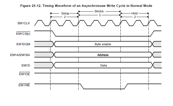
Hello there. From the figure above I see there is the EM1DQM (byte enable) signal.  I’ve got an FPGA connected to the Delfino, Tms320f28375D, via the emif; and there’s a memory array inside the FPGA that I’d like the Delfino to be able to write and read to.

Q1) My question is: Do I need to use the EM1DQM to qualify the EM1D (Data bus) along with the chipselect and the wen to write the data into the FPGA’s memory?

Or is it enough to just use the wen alone and do the write of the emif databus when the wen is active low?


Q2) Do I need the byte enables during an emif read?


Thank you for your help,

  • Hi Shawn,

    Are you using 16bit interface or 32bit interface? For 16bit it's not needed (because minimum access from C28x is 16bit but for 32bit, you'll need it.

    For READ it's not needed. It's output from EMIF to it knows what is valid data.

    Regards,
    Vivek Singh
  • Thank you very much!

    I’ve got a few more questions for you below:

    Q3) If the byte enables are used during a write, when would they be asserted normally – in the setup phase or strobe phase in Fig 25-12?
    Also, since they are being used is there a minimum setting for the Fig 25-12 that should be used in the async_CSn_CR? Or can I use the timing specified in Fig 25-12 for the async write?

    Q4) If I latch the emif address on the instant when the CSn edge goes low during the setup is there going to be any issue with getting the correct address or is it better to latch the address on the last clk of the setup phase?

    Q5) For an emif async access, regarding the setup of the emif is the async_CSn_CR the only register I have to modify? Or are there other registers?

    Q6) For an async emif access will the EM1CLK always be driven out of the EM1CLK pin of the DSP?

    Q7) For an async emif access if the emif bus is inactive will the DSP drive out logic high on CS0n, CS3n, and CS4n or do I have to have pullup resistors on them on the pcb?

    Q8) Also, If I am switching between writing to CS0n, CS2n, CS3n, CS4n in the Delfino memory map I’m assuming I don’t have to do anything special other than a direct write to those memory mapped regions? I’ve got an SDRAM chip on CS0n and the FPGA on CS3n and CS4n so the dsp engineer is alternating DSP accesses to the SDRAM and FPGA.
  • Hi Shawn,

    Q3) If the byte enables are used during a write, when would they be asserted normally – in the setup phase or strobe phase in Fig 25-12?
    Also, since they are being used is there a minimum setting for the Fig 25-12 that should be used in the async_CSn_CR? Or can I use the timing specified in Fig 25-12 for the async write?


    This info if given in timing diagram in datasheet. It remains active during full write cycle.

    Q4) If I latch the emif address on the instant when the CSn edge goes low during the setup is there going to be any issue with getting the correct address or is it better to latch the address on the last clk of the setup phase?

    I would recommend latching it during end of setup phase.

    Q5) For an emif async access, regarding the setup of the emif is the async_CSn_CR the only register I have to modify? Or are there other registers?

    Most of the settings are in this register only. If using WAIT feature then need to configure another register. Please also refer controlSUITE example "emif1_16bit_asram".

    Q6) For an async emif access will the EM1CLK always be driven out of the EM1CLK pin of the DSP?

    Since it's ASYNC interface, clock is not needed but if user configures the pinmux to the clock (e.g. EM1CLK) will be available. Please note that none of the ASYNC timings are wrt to this clock. Also if operating the EMIF at 200MHz then clock will not be stable due to high frq (IO supports 100MHz max).

    Q7) For an async emif access if the emif bus is inactive will the DSP drive out logic high on CS0n, CS3n, and CS4n or do I have to have pullup resistors on them on the pcb?

    DSP will drive CSx pin inactive.

    Q8) Also, If I am switching between writing to CS0n, CS2n, CS3n, CS4n in the Delfino memory map I’m assuming I don’t have to do anything special other than a direct write to those memory mapped regions? I’ve got an SDRAM chip on CS0n and the FPGA on CS3n and CS4n so the dsp engineer is alternating DSP accesses to the SDRAM and FPGA.

    That is correct. 

    Regards,

    Vivek Singh