This thread has been locked.

If you have a related question, please click the "Ask a related question" button in the top right corner. The newly created question will be automatically linked to this question.

TMS320F28377S: Async reset of CMPSS latched output.

Part Number: TMS320F28377S

Hello.

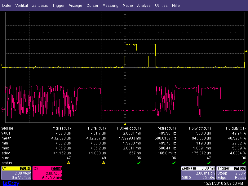
I'm using TMS320F28377S Launchpad (LAUNCHXL-F28377S) to generate a PWM signal with 500Hz and 50% duty cycle. I want to trip it cycle by cycle with a CMPSS latched output. I've attached the CCS project. As you can see on the osciloscop screenshot the tripping is working, but I expected that the latched output from CMPSS will not be be resetted because I've not configured any PWMSync output. The latched CMPSS output gets resetted somewhen (randomly?).
RED: CMPSS latched output.

YELLOW: PWM output.

Why is this so?

Regards

Christian

CMPSS_Latch.zip

  • Christian,

    The CMPSS output latch is fed by the Digital Filter.  Did you configure the Digital Filter?

    -Tommy

  • Tommy,

    No I didn't. But now I've tried it and the result is the same.

    Regards

    Christian

  • Christian,

    Can you attach your updated main.c with the digital filter configured?

    -Tommy

  • Here it is:

    /*
     * main.c
     */
    #include "F2837xS_device.h"
    #include "F28x_Project.h"
    #include "pinmux.h"
    
    static void InitPWM(void);
    static void InitCMPSS1(void);
    
    int main(void)
    {
       InitSysCtrl();
       GPIO_setPinMuxConfig();
       InitPWM();
    
       /* Output the CMPSS output to GPIO17. */
       EALLOW;
       OutputXbarRegs.OUTPUT8MUX0TO15CFG.bit.MUX0 = 1;
       OutputXbarRegs.OUTPUT8MUXENABLE.bit.MUX0 = 1;
       EDIS;
    
       InitCMPSS1();
    
       /* Generate a 500Hz 50% PWM signal. */
       EPwm2Regs.TBPRD = 49999;
       EPwm2Regs.CMPA.bit.CMPA = 0;
       EPwm2Regs.CMPB.bit.CMPB = 25000;
       EPwm2Regs.AQCTLA.bit.CAU = AQ_SET;
       EPwm2Regs.AQCTLA.bit.CBU = AQ_CLEAR;
       EPwm2Regs.DBCTL.bit.OUT_MODE = DB_FULL_ENABLE;
    
       EALLOW;
       EPwmXbarRegs.TRIP4MUX0TO15CFG.bit.MUX0 = 1;
       EPwmXbarRegs.TRIP4MUXENABLE.bit.MUX0 = 1;
    
       EPwm2Regs.DCTRIPSEL.bit.DCBHCOMPSEL = 0xF; // select trip combination input (DCBHTRIPSEL register)
       EPwm2Regs.TZDCSEL.bit.DCBEVT2 = TZ_DCBH_HI;
       EPwm2Regs.TZSEL.bit.DCBEVT2 = 1;
       EPwm2Regs.DCBHTRIPSEL.bit.TRIPINPUT4 = 1;
       EDIS;
    
       while (1)
          ;
    }
    
    static void InitPWM()
    {
       EALLOW;
       EPwm2Regs.TBPRD = 0xFFFF;
       EPwm2Regs.TBPHS.bit.TBPHS = 0x0000;           // Phase is 0
       EPwm2Regs.TBCTR = 0x0000;                     // Clear counter
    
       /* Setup TBCLK. */
       EPwm2Regs.TBCTL.bit.CTRMODE = TB_COUNT_UP; // Count up
       EPwm2Regs.TBCTL.bit.PHSEN = TB_DISABLE;        // Disable phase loading
       /* Select division by 2*2. So TBCLK = 100MHz/4 = 25MHz. */
       EPwm2Regs.TBCTL.bit.HSPCLKDIV = TB_DIV2;
       EPwm2Regs.TBCTL.bit.CLKDIV = TB_DIV2;
    
       /* Setup compare. */
       EPwm2Regs.CMPA.bit.CMPA = 0;
       EPwm2Regs.CMPB.bit.CMPB = 0;
    
       /* Action qualifier module uses shadow registers. */
       EPwm2Regs.AQCTL.bit.SHDWAQAMODE = 1;
       EPwm2Regs.AQCTL.bit.SHDWAQBMODE = 1;
       /* Set actions. */
       EPwm2Regs.AQCTLA.bit.CAU = AQ_NO_ACTION;
       EPwm2Regs.AQCTLA.bit.CBU = AQ_NO_ACTION;
    
       EPwm2Regs.AQCTLB.bit.CAU = AQ_NO_ACTION;
       EPwm2Regs.AQCTLB.bit.CBU = AQ_NO_ACTION;
    
       /* Activate deadband shadow register load at counter = 0. */
       EPwm2Regs.DBCTL2.bit.SHDWDBCTLMODE = 1;
       /* Active High complementary PWMs - setup the deadband. */
       EPwm2Regs.DBCTL.bit.IN_MODE = DBA_ALL;
       /* Always invert ePWMB output. */
       EPwm2Regs.DBCTL.bit.POLSEL = DB_ACTV_HIC;
       EPwm2Regs.DBRED.bit.DBRED = 0;
       EPwm2Regs.DBFED.bit.DBFED = 0;
    
       EPwm2Regs.TZCTL.bit.TZA = TZ_FORCE_LO;
       EPwm2Regs.TZCTL.bit.TZB = TZ_FORCE_LO;
       EDIS;
    }
    
    static void InitCMPSS1()
    {
       EALLOW;
       Cmpss1Regs.COMPSTSCLR.bit.HSYNCCLREN = 1;
       Cmpss1Regs.COMPSTSCLR.bit.LSYNCCLREN = 1;
       /* Lower threshold comparator must be inverted. */
       Cmpss1Regs.COMPCTL.bit.COMPLINV = 1;
       Cmpss1Regs.DACHVALS.all = 4095;
       Cmpss1Regs.DACLVALS.all = 0;
       Cmpss1Regs.COMPCTL.bit.COMPDACE = 1;
       /* DAC needs some time for powering up. */
       DELAY_US(20);
       Cmpss1Regs.CTRIPHFILCTL.bit.SAMPWIN = 4;
       Cmpss1Regs.CTRIPHFILCTL.bit.THRESH = 3;
       Cmpss1Regs.CTRIPLFILCTL.bit.SAMPWIN = 4;
       Cmpss1Regs.CTRIPLFILCTL.bit.THRESH = 3;
       Cmpss1Regs.CTRIPHFILCTL.bit.FILINIT = 1;
       Cmpss1Regs.CTRIPLFILCTL.bit.FILINIT = 1;
    
       Cmpss1Regs.COMPSTSCLR.bit.HLATCHCLR = 1;
       Cmpss1Regs.COMPSTSCLR.bit.LLATCHCLR = 1;
    
       Cmpss1Regs.COMPCTL.bit.ASYNCHEN = 1;
       Cmpss1Regs.COMPCTL.bit.ASYNCLEN = 1;
       Cmpss1Regs.COMPCTL.bit.CTRIPHSEL = 3;
       Cmpss1Regs.COMPCTL.bit.CTRIPLSEL = 3;
       Cmpss1Regs.COMPCTL.bit.CTRIPOUTHSEL = 3;
       Cmpss1Regs.COMPCTL.bit.CTRIPOUTLSEL = 3;
       EDIS;
    }
    

  • Christian,

    Thanks for the reference code. Can you check on a couple of things:

    1. Your X-BAR Output configuration will send the OR'd value of CTRIPOUTH and CTRIPOUTL to the pin. I think this is what you want, but I would like to confirm.
    2. Your DACVALS values (High=4095; Low=0) will make it very difficult for the comparators to trip. Can you try a mid-point 2048 for debug? Otherwise, the comparators would only trip because either:
      1. The DAC offset & gain errors produce imperfect reference voltages near VSSA and VDDA/VDAC, or
      2. The comparator inputs are driven below VSSA or above VDDA/VDAC

    Your observations might be explained if the comparators are having a difficult time qualifying a trip because of (2) above.  The spurious trips are passed through to the X-BAR because the ASYNC path is enabled, but the Latch is never set because the trips are too short to be qualified by the Digital Filter.

    -Tommy

  • Tommy.

    Sorry for my late Response, I was not in office yesterday.

    1. Yes thats my intention. But I only route the CTRIPOUTH and CTRIPOUTL to a pin to see the comparator state on an osci.

    2. I've tried an upper level at 2048 and lower level at 1024 with the same result. => The latch will always be resetted by someone.

    I've attached the new main.c file.

    /*
     * main.c
     */
    #include "F2837xS_device.h"
    #include "F28x_Project.h"
    #include "pinmux.h"
    
    static void InitPWM(void);
    static void InitCMPSS1(void);
    
    int main(void)
    {
       InitSysCtrl();
       GPIO_setPinMuxConfig();
       InitPWM();
    
       /* Output the CMPSS output to GPIO17. */
       EALLOW;
       OutputXbarRegs.OUTPUT8MUX0TO15CFG.bit.MUX0 = 1;
       OutputXbarRegs.OUTPUT8MUXENABLE.bit.MUX0 = 1;
       EDIS;
    
       InitCMPSS1();
    
       /* Generate a 500Hz 50% PWM signal. */
       EPwm2Regs.TBPRD = 49999;
       EPwm2Regs.CMPA.bit.CMPA = 0;
       EPwm2Regs.CMPB.bit.CMPB = 25000;
       EPwm2Regs.AQCTLA.bit.CAU = AQ_SET;
       EPwm2Regs.AQCTLA.bit.CBU = AQ_CLEAR;
       EPwm2Regs.DBCTL.bit.OUT_MODE = DB_FULL_ENABLE;
    
       EALLOW;
       EPwmXbarRegs.TRIP4MUX0TO15CFG.bit.MUX0 = 1;
       EPwmXbarRegs.TRIP4MUXENABLE.bit.MUX0 = 1;
    
       EPwm2Regs.DCTRIPSEL.bit.DCBHCOMPSEL = 0xF; // select trip combination input (DCBHTRIPSEL register)
       EPwm2Regs.TZDCSEL.bit.DCBEVT2 = TZ_DCBH_HI;
       EPwm2Regs.TZSEL.bit.DCBEVT2 = 1;
       EPwm2Regs.DCBHTRIPSEL.bit.TRIPINPUT4 = 1;
       EDIS;
    
       while (1)
          ;
    }
    
    static void InitPWM()
    {
       EALLOW;
       EPwm2Regs.TBPRD = 0xFFFF;
       EPwm2Regs.TBPHS.bit.TBPHS = 0x0000;           // Phase is 0
       EPwm2Regs.TBCTR = 0x0000;                     // Clear counter
    
       /* Setup TBCLK. */
       EPwm2Regs.TBCTL.bit.CTRMODE = TB_COUNT_UP; // Count up
       EPwm2Regs.TBCTL.bit.PHSEN = TB_DISABLE;        // Disable phase loading
       /* Select division by 2*2. So TBCLK = 100MHz/4 = 25MHz. */
       EPwm2Regs.TBCTL.bit.HSPCLKDIV = TB_DIV2;
       EPwm2Regs.TBCTL.bit.CLKDIV = TB_DIV2;
    
       /* Setup compare. */
       EPwm2Regs.CMPA.bit.CMPA = 0;
       EPwm2Regs.CMPB.bit.CMPB = 0;
    
       /* Action qualifier module uses shadow registers. */
       EPwm2Regs.AQCTL.bit.SHDWAQAMODE = 1;
       EPwm2Regs.AQCTL.bit.SHDWAQBMODE = 1;
       /* Set actions. */
       EPwm2Regs.AQCTLA.bit.CAU = AQ_NO_ACTION;
       EPwm2Regs.AQCTLA.bit.CBU = AQ_NO_ACTION;
    
       EPwm2Regs.AQCTLB.bit.CAU = AQ_NO_ACTION;
       EPwm2Regs.AQCTLB.bit.CBU = AQ_NO_ACTION;
    
       /* Activate deadband shadow register load at counter = 0. */
       EPwm2Regs.DBCTL2.bit.SHDWDBCTLMODE = 1;
       /* Active High complementary PWMs - setup the deadband. */
       EPwm2Regs.DBCTL.bit.IN_MODE = DBA_ALL;
       /* Always invert ePWMB output. */
       EPwm2Regs.DBCTL.bit.POLSEL = DB_ACTV_HIC;
       EPwm2Regs.DBRED.bit.DBRED = 0;
       EPwm2Regs.DBFED.bit.DBFED = 0;
    
       EPwm2Regs.TZCTL.bit.TZA = TZ_FORCE_LO;
       EPwm2Regs.TZCTL.bit.TZB = TZ_FORCE_LO;
       EDIS;
    }
    
    static void InitCMPSS1()
    {
       EALLOW;
       Cmpss1Regs.COMPSTSCLR.bit.HSYNCCLREN = 1;
       Cmpss1Regs.COMPSTSCLR.bit.LSYNCCLREN = 1;
       /* Lower threshold comparator must be inverted. */
       Cmpss1Regs.COMPCTL.bit.COMPLINV = 1;
       Cmpss1Regs.DACHVALS.all = 2048;
       Cmpss1Regs.DACLVALS.all = 1024;
       Cmpss1Regs.COMPCTL.bit.COMPDACE = 1;
       /* DAC needs some time for powering up. */
       DELAY_US(20);
       Cmpss1Regs.CTRIPHFILCTL.bit.SAMPWIN = 4;
       Cmpss1Regs.CTRIPHFILCTL.bit.THRESH = 3;
       Cmpss1Regs.CTRIPLFILCTL.bit.SAMPWIN = 4;
       Cmpss1Regs.CTRIPLFILCTL.bit.THRESH = 3;
       Cmpss1Regs.CTRIPHFILCTL.bit.FILINIT = 1;
       Cmpss1Regs.CTRIPLFILCTL.bit.FILINIT = 1;
    
       Cmpss1Regs.COMPSTSCLR.bit.HLATCHCLR = 1;
       Cmpss1Regs.COMPSTSCLR.bit.LLATCHCLR = 1;
    
       Cmpss1Regs.COMPCTL.bit.ASYNCHEN = 1;
       Cmpss1Regs.COMPCTL.bit.ASYNCLEN = 1;
       Cmpss1Regs.COMPCTL.bit.CTRIPHSEL = 3;
       Cmpss1Regs.COMPCTL.bit.CTRIPLSEL = 3;
       Cmpss1Regs.COMPCTL.bit.CTRIPOUTHSEL = 3;
       Cmpss1Regs.COMPCTL.bit.CTRIPOUTLSEL = 3;
       EDIS;
    }
    

    Thanks and Regards

    Christian

  • Christian,

    I tried your code on my setup and I think the problem could be with enabling the COMPSTSCLR_xSYNCCLREN path without configuring the EPWM PWMSYNC.

    Can you try either disabling the COMPSTSCLR_xSYNCCLREN paths or selecting an active EPWM (like EPWM2 in your example) as the RAMPSOURCE PWMSYNC?

    -Tommy

  • Tommy,

    Disabling the COMPSTSCLR_xSYNCCLREN path helps. But I try to trip the PWM signal on a Cycle-by-Cycle Basis as descibed in chapter 13.11.3 of the Delfino datasheet. I will also try the blanking window method, hopefully this works.

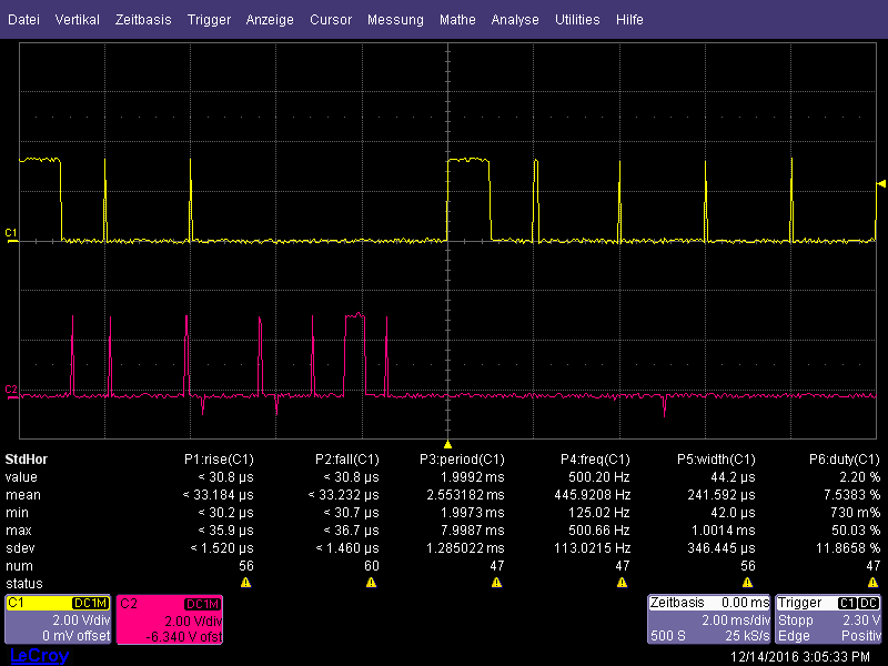
    I also tried to select ePWM2 as RAMPSOURCE. This makes it better a little bit, sometimes the comparator output gets latched, but most of the time not. See the attached osci screenshot.

    Also please find the main.c file here:

    /*
     * main.c
     */
    #include "F2837xS_device.h"
    #include "F28x_Project.h"
    #include "pinmux.h"
    
    static void InitPWM(void);
    static void InitCMPSS1(void);
    
    int main(void)
    {
        InitSysCtrl();
        GPIO_setPinMuxConfig();
        InitPWM();
    
        /* Output the CMPSS output to GPIO17. */
        EALLOW;
        OutputXbarRegs.OUTPUT8MUX0TO15CFG.bit.MUX0 = 1;
        OutputXbarRegs.OUTPUT8MUXENABLE.bit.MUX0 = 1;
        EDIS;
    
        InitCMPSS1();
    
        /* Generate a 500Hz 50% PWM signal. */
        EPwm2Regs.TBPRD = 49999;
        EPwm2Regs.CMPA.bit.CMPA = 0;
        EPwm2Regs.CMPB.bit.CMPB = 25000;
        EPwm2Regs.AQCTLA.bit.CAU = AQ_SET;
        EPwm2Regs.AQCTLA.bit.CBU = AQ_CLEAR;
        EPwm2Regs.DBCTL.bit.OUT_MODE = DB_FULL_ENABLE;
    
        EALLOW;
        EPwmXbarRegs.TRIP4MUX0TO15CFG.bit.MUX0 = 1;
        EPwmXbarRegs.TRIP4MUXENABLE.bit.MUX0 = 1;
    
        EPwm2Regs.DCTRIPSEL.bit.DCBHCOMPSEL = 0xF; // select trip combination input (DCBHTRIPSEL register)
        EPwm2Regs.TZDCSEL.bit.DCBEVT2 = TZ_DCBH_HI;
        EPwm2Regs.TZSEL.bit.DCBEVT2 = 1;
        EPwm2Regs.DCBHTRIPSEL.bit.TRIPINPUT4 = 1;
        EDIS;
    
        while (1)
            ;
    }
    
    static void InitPWM()
    {
        EALLOW;
        EPwm2Regs.TBPRD = 0xFFFF;
        EPwm2Regs.TBPHS.bit.TBPHS = 0x0000;           // Phase is 0
        EPwm2Regs.TBCTR = 0x0000;                     // Clear counter
    
        /* Setup TBCLK. */
        EPwm2Regs.TBCTL.bit.CTRMODE = TB_COUNT_UP; // Count up
        EPwm2Regs.TBCTL.bit.PHSEN = TB_DISABLE;        // Disable phase loading
        /* Select division by 2*2. So TBCLK = 100MHz/4 = 25MHz. */
        EPwm2Regs.TBCTL.bit.HSPCLKDIV = TB_DIV2;
        EPwm2Regs.TBCTL.bit.CLKDIV = TB_DIV2;
    
        /* Setup compare. */
        EPwm2Regs.CMPA.bit.CMPA = 0;
        EPwm2Regs.CMPB.bit.CMPB = 0;
    
        /* Action qualifier module uses shadow registers. */
        EPwm2Regs.AQCTL.bit.SHDWAQAMODE = 1;
        EPwm2Regs.AQCTL.bit.SHDWAQBMODE = 1;
        /* Set actions. */
        EPwm2Regs.AQCTLA.bit.CAU = AQ_NO_ACTION;
        EPwm2Regs.AQCTLA.bit.CBU = AQ_NO_ACTION;
    
        EPwm2Regs.AQCTLB.bit.CAU = AQ_NO_ACTION;
        EPwm2Regs.AQCTLB.bit.CBU = AQ_NO_ACTION;
    
        /* Activate deadband shadow register load at counter = 0. */
        EPwm2Regs.DBCTL2.bit.SHDWDBCTLMODE = 1;
        /* Active High complementary PWMs - setup the deadband. */
        EPwm2Regs.DBCTL.bit.IN_MODE = DBA_ALL;
        /* Always invert ePWMB output. */
        EPwm2Regs.DBCTL.bit.POLSEL = DB_ACTV_HIC;
        EPwm2Regs.DBRED.bit.DBRED = 0;
        EPwm2Regs.DBFED.bit.DBFED = 0;
    
        EPwm2Regs.TZCTL.bit.TZA = TZ_FORCE_LO;
        EPwm2Regs.TZCTL.bit.TZB = TZ_FORCE_LO;
        EDIS;
    }
    
    static void InitCMPSS1()
    {
        EALLOW;
        Cmpss1Regs.COMPSTSCLR.bit.HSYNCCLREN = 1;
        Cmpss1Regs.COMPSTSCLR.bit.LSYNCCLREN = 1;
        /* Lower threshold comparator must be inverted. */
        Cmpss1Regs.COMPCTL.bit.COMPLINV = 1;
        Cmpss1Regs.DACHVALS.all = 2048;
        Cmpss1Regs.DACLVALS.all = 1024;
        Cmpss1Regs.COMPCTL.bit.COMPDACE = 1;
        /* DAC needs some time for powering up. */
        DELAY_US(20);
        Cmpss1Regs.CTRIPHFILCTL.bit.SAMPWIN = 4;
        Cmpss1Regs.CTRIPHFILCTL.bit.THRESH = 3;
        Cmpss1Regs.CTRIPLFILCTL.bit.SAMPWIN = 4;
        Cmpss1Regs.CTRIPLFILCTL.bit.THRESH = 3;
        Cmpss1Regs.CTRIPHFILCTL.bit.FILINIT = 1;
        Cmpss1Regs.CTRIPLFILCTL.bit.FILINIT = 1;
    
        Cmpss1Regs.COMPSTSCLR.bit.HLATCHCLR = 1;
        Cmpss1Regs.COMPSTSCLR.bit.LLATCHCLR = 1;
    
        Cmpss1Regs.COMPCTL.bit.ASYNCHEN = 1;
        Cmpss1Regs.COMPCTL.bit.ASYNCLEN = 1;
        Cmpss1Regs.COMPCTL.bit.CTRIPHSEL = 3;
        Cmpss1Regs.COMPCTL.bit.CTRIPLSEL = 3;
        Cmpss1Regs.COMPCTL.bit.CTRIPOUTHSEL = 3;
        Cmpss1Regs.COMPCTL.bit.CTRIPOUTLSEL = 3;
        Cmpss1Regs.COMPDACCTL.bit.RAMPSOURCE = 1;
        EDIS;
    }
    

    Regards

    Christian

  • Christian,

    The comparator output seems to be oscillating a lot.  Can you change the CTRIPOUT monitor signal source from selection 3 (Latch) to selection 2 (Digital Filter) and see how the filtered signal compares to your expectations?  The filter might be removing the shorter trip events.

    Also, would you be able to scope the comparator input signal?  It is difficult for me to judge whether the comparator output is valid or not without an input signal for reference.

    -Tommy

  • Tommy.

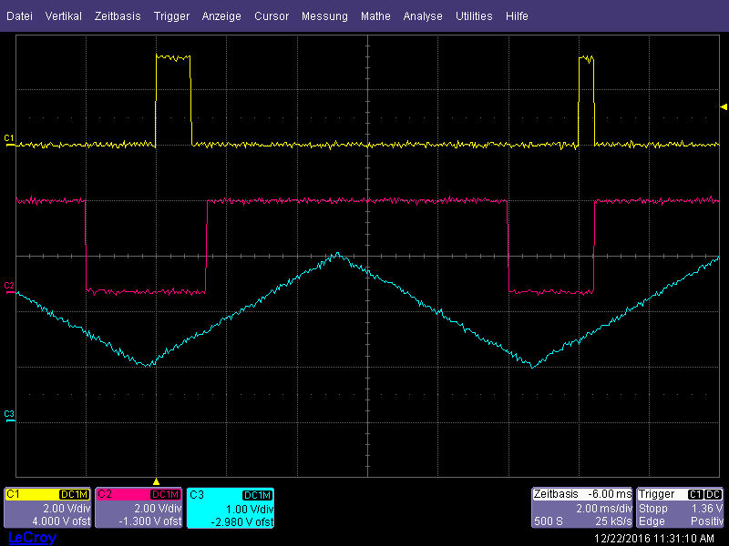
    This helped. It's also working if I disable the async input (ASYNCHEN = 0). The I get this beautiful osci screenshot.

    Yellow: PWM

    Red: Comparator output

    Blue: Voltage to comparator Input.

    One problem still exists: The reset of the comparator latch will be done at PWM period start (CTR=0) as you can see in the osci screenshot. In software I have configured SYNCOSEL in TBCTL register to 2, which means a sync pulse will be generated if CTR=CMPB (=12500). Do I miss something else to configure?

    Thanks

    Regards

    Christian

    PS: Here is the new main.c

    /*
     * main.c
     */
    #include "F2837xS_device.h"
    #include "F28x_Project.h"
    #include "pinmux.h"
    
    static void InitPWM(void);
    static void InitCMPSS1(void);
    
    int main(void)
    {
       InitSysCtrl();
       GPIO_setPinMuxConfig();
       InitPWM();
    
       /* Output the CMPSS output to GPIO17. */
       EALLOW;
       OutputXbarRegs.OUTPUT8MUX0TO15CFG.bit.MUX0 = 1;
       OutputXbarRegs.OUTPUT8MUXENABLE.bit.MUX0 = 1;
       EDIS;
    
       InitCMPSS1();
    
       /* Generate a 500Hz 50% PWM signal. */
       EPwm2Regs.TBPRD = 49999;
       EPwm2Regs.CMPA.bit.CMPA = 0;
       EPwm2Regs.CMPB.bit.CMPB = 25000;
       EPwm2Regs.AQCTLA.bit.CAU = AQ_SET;
       EPwm2Regs.AQCTLA.bit.CBU = AQ_CLEAR;
       EPwm2Regs.DBCTL.bit.OUT_MODE = DB_FULL_ENABLE;
    
       EALLOW;
       EPwmXbarRegs.TRIP4MUX0TO15CFG.bit.MUX0 = 1;
       EPwmXbarRegs.TRIP4MUXENABLE.bit.MUX0 = 1;
    
       EPwm2Regs.DCTRIPSEL.bit.DCBHCOMPSEL = 0xF; // select trip combination input (DCBHTRIPSEL register)
       EPwm2Regs.TZDCSEL.bit.DCBEVT2 = TZ_DCBH_HI;
       EPwm2Regs.TZSEL.bit.DCBEVT2 = 1;
       EPwm2Regs.DCBHTRIPSEL.bit.TRIPINPUT4 = 1;
       EDIS;
    
       while (1)
          ;
    }
    
    static void InitPWM()
    {
       EALLOW;
       EPwm2Regs.TBPRD = 0xFFFF;
       EPwm2Regs.TBPHS.bit.TBPHS = 0x0000;           // Phase is 0
       EPwm2Regs.TBCTR = 0x0000;                     // Clear counter
    
       /* Setup TBCLK. */
       EPwm2Regs.TBCTL.bit.CTRMODE = TB_COUNT_UP; // Count up
       EPwm2Regs.TBCTL.bit.PHSEN = TB_DISABLE;        // Disable phase loading
       /* Select division by 2*2. So TBCLK = 100MHz/4 = 25MHz. */
       EPwm2Regs.TBCTL.bit.HSPCLKDIV = TB_DIV2;
       EPwm2Regs.TBCTL.bit.CLKDIV = TB_DIV2;
    
       /* Setup compare. */
       EPwm2Regs.CMPA.bit.CMPA = 0;
       EPwm2Regs.CMPB.bit.CMPB = 0;
    
       /* Action qualifier module uses shadow registers. */
       EPwm2Regs.AQCTL.bit.SHDWAQAMODE = 1;
       EPwm2Regs.AQCTL.bit.SHDWAQBMODE = 1;
       /* Set actions. */
       EPwm2Regs.AQCTLA.bit.CAU = AQ_NO_ACTION;
       EPwm2Regs.AQCTLA.bit.CBU = AQ_NO_ACTION;
    
       EPwm2Regs.AQCTLB.bit.CAU = AQ_NO_ACTION;
       EPwm2Regs.AQCTLB.bit.CBU = AQ_NO_ACTION;
    
       /* Activate deadband shadow register load at counter = 0. */
       EPwm2Regs.DBCTL2.bit.SHDWDBCTLMODE = 1;
       /* Active High complementary PWMs - setup the deadband. */
       EPwm2Regs.DBCTL.bit.IN_MODE = DBA_ALL;
       /* Always invert ePWMB output. */
       EPwm2Regs.DBCTL.bit.POLSEL = DB_ACTV_HIC;
       EPwm2Regs.DBRED.bit.DBRED = 0;
       EPwm2Regs.DBFED.bit.DBFED = 0;
    
       EPwm2Regs.TZCTL.bit.TZA = TZ_FORCE_LO;
       EPwm2Regs.TZCTL.bit.TZB = TZ_FORCE_LO;
    
       /* Generate a PWM Sync signal if CTR=CMPB. */
       EPwm2Regs.TBCTL.bit.SYNCOSEL = 2;
       EDIS;
    }
    
    static void InitCMPSS1()
    {
       EALLOW;
       Cmpss1Regs.COMPSTSCLR.bit.HSYNCCLREN = 1;
       Cmpss1Regs.COMPSTSCLR.bit.LSYNCCLREN = 1;
       /* Lower threshold comparator must be inverted. */
       Cmpss1Regs.COMPCTL.bit.COMPLINV = 1;
       Cmpss1Regs.DACHVALS.all = 2048;
       Cmpss1Regs.DACLVALS.all = 1024;
       Cmpss1Regs.COMPCTL.bit.COMPDACE = 1;
       /* DAC needs some time for powering up. */
       DELAY_US(20);
       Cmpss1Regs.CTRIPHFILCTL.bit.SAMPWIN = 0x1F;
       Cmpss1Regs.CTRIPHFILCTL.bit.THRESH = 0x1E;
       Cmpss1Regs.CTRIPLFILCTL.bit.SAMPWIN = 0x1F;
       Cmpss1Regs.CTRIPLFILCTL.bit.THRESH = 0x1E;
       Cmpss1Regs.CTRIPHFILCTL.bit.FILINIT = 1;
       Cmpss1Regs.CTRIPLFILCTL.bit.FILINIT = 1;
    
       Cmpss1Regs.COMPSTSCLR.bit.HLATCHCLR = 1;
       Cmpss1Regs.COMPSTSCLR.bit.LLATCHCLR = 1;
    
       Cmpss1Regs.COMPCTL.bit.ASYNCHEN = 0;
       Cmpss1Regs.COMPCTL.bit.ASYNCLEN = 0;
       Cmpss1Regs.COMPCTL.bit.CTRIPHSEL = 3;
       Cmpss1Regs.COMPCTL.bit.CTRIPLSEL = 3;
       Cmpss1Regs.COMPCTL.bit.CTRIPOUTHSEL = 3;
       Cmpss1Regs.COMPCTL.bit.CTRIPOUTLSEL = 3;
       Cmpss1Regs.COMPDACCTL.bit.RAMPSOURCE = 1;
       EDIS;
    }
    

  • Christian,

    Glad that you made some progress.

    I think you may want to try setting the PWMSYNC generation using CMPC or CMPD via HRPCTL[PWMSYNCSELX].

    I noticed that you increased the filter window quite a bit.  You might miss some LATCH resets because of the issue described in the "CMPSS: COMPxLATCH May Not Clear Properly Under Certain Conditions" advisory.

    Can you try to observe the filter output with SAMPWIN and THRESH set to 0?  Instead of using the digital filter to screen out the high-frequency oscillations, try using different hysteresis settings in COMPHYSCTL.  It looks to me like the oscillations might be caused by the small noise band on top of your input signal.  Hysteresis should be able to help with that.

    -Tommy

  • Tommy.

    I'm now going to christmas holidays for two weeks. I will continue experimenting next year.
    Thank you for your help so far.
    I wish you a Merry Christmas and a Happy New Year.

    Regards
    Christian
  • Thanks Christian.  Merry Christmas and Happy New Year to you too!

  • Hi.

    I've found a solution which works for me if I do not write to CMPA, CMPB, AQCTLA.CAU or AQCTLA.CBU registers.

    If I update one of these registers in the PWM ISR then the comparator latch isn't working. I do not find out why? Is there any known issue about that?

    Thanks

    Regards

    Christian

  • Christian,

    I am not aware of any usage issues between the PWM registers and CMPSS latch.

    Is this a temporary failure that returns to normal after a couple of cycles or does the latch break until reset?

    -Tommy

  • Tommy.

    Forget my last post. It has nothing to do with PWM register write. Now I know what is happening in my use case. I try to explain:

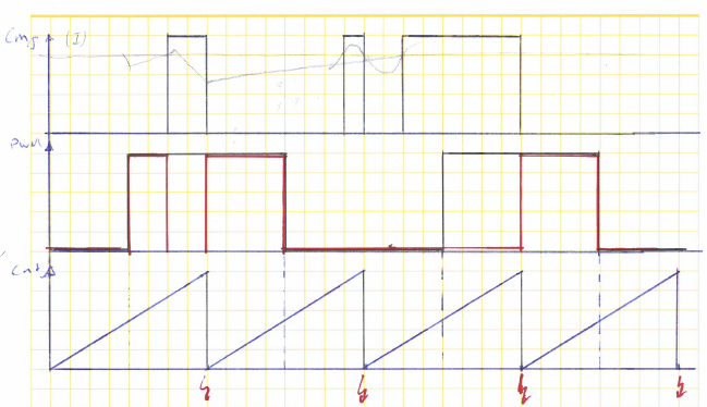
    I've setup a up-counter for PWM generation. Everytime the counter gets reset to zero I have an Interrupt. I setup the CMPA and AQ register for rising edge in every even interrupt and for falling egde in every odd interrupt. So I have a counter=zero event during the high period of the PWM signal which resets the comparator latch. The resulting PWM signal looks like this (red waveform):

    But thats not what I want. In my case the comparator latch shall be reseted at CMPA.

    Is that possible, or is there another way to do this?

    Regards

    Christian

  • Hi again.

    I've found a solution that works for me. I reset the comparator latch 10 ticks after counter = 0 by generating a PWM sync at CMPC = 10. So I get the behaviour I want:

    Thank you for your help.

    BR

    Christian

  • Christian,

    I'm glad that it's working for you now.  I was going to recommend using CMPC or CMPD to generate your PWMSYNC signal, but you discovered it first.

    -Tommy